
Hyper-FET’s Phase-Transition-Materials Design Guidelines for Ultra-Low Power Applications at 3 nm Technology Node

 , ,
, ,
Abstract
:1. Introduction
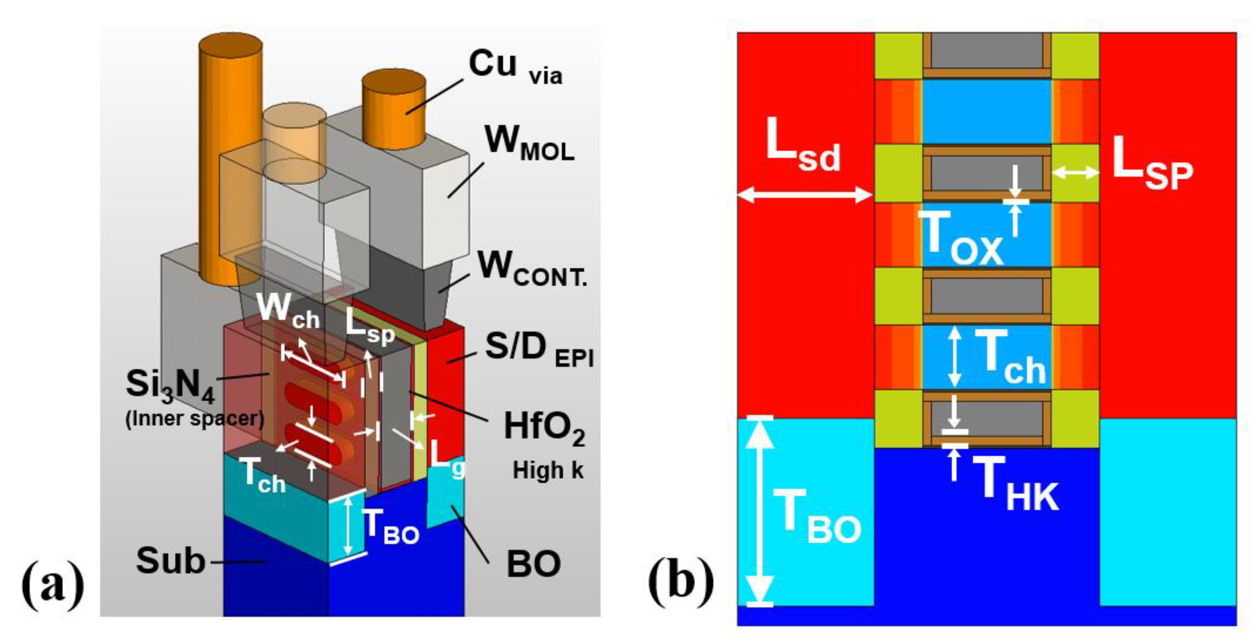
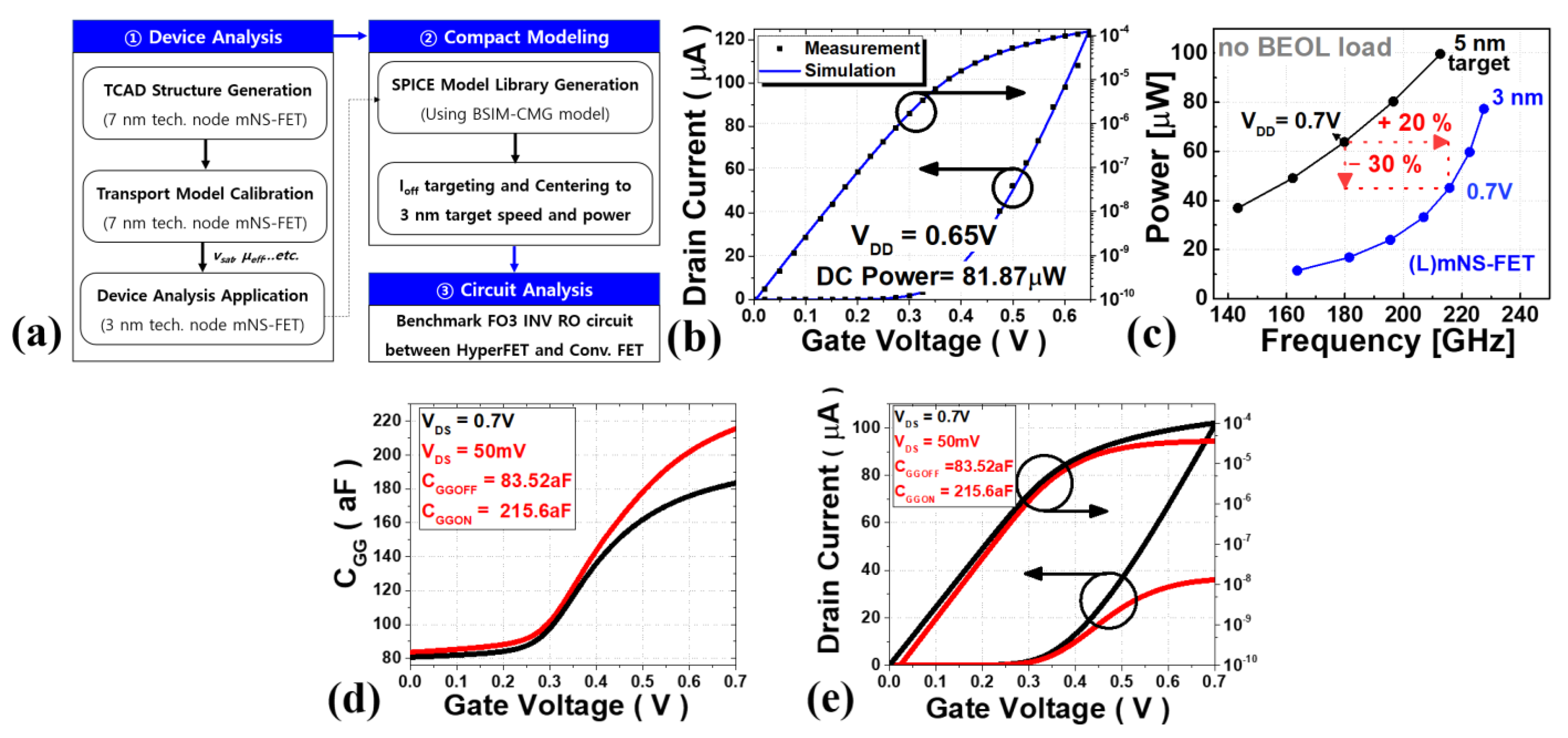
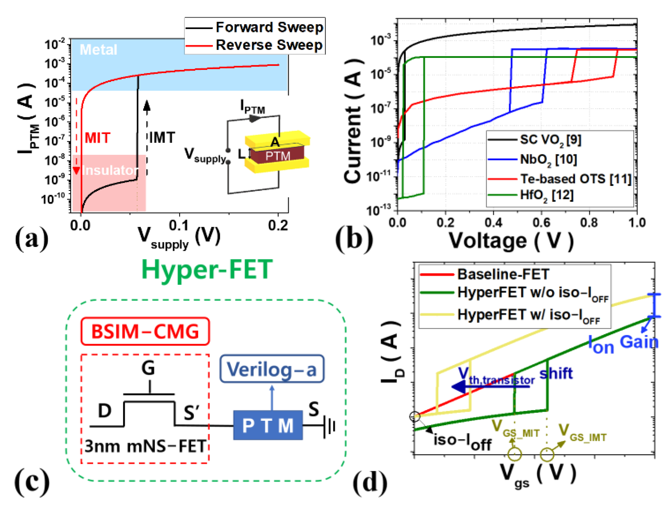
2. Simulation Environment for Hyper-FET Device and Circuit Co-Analysis
3. Hyper-FET Simulation Results and Discussions
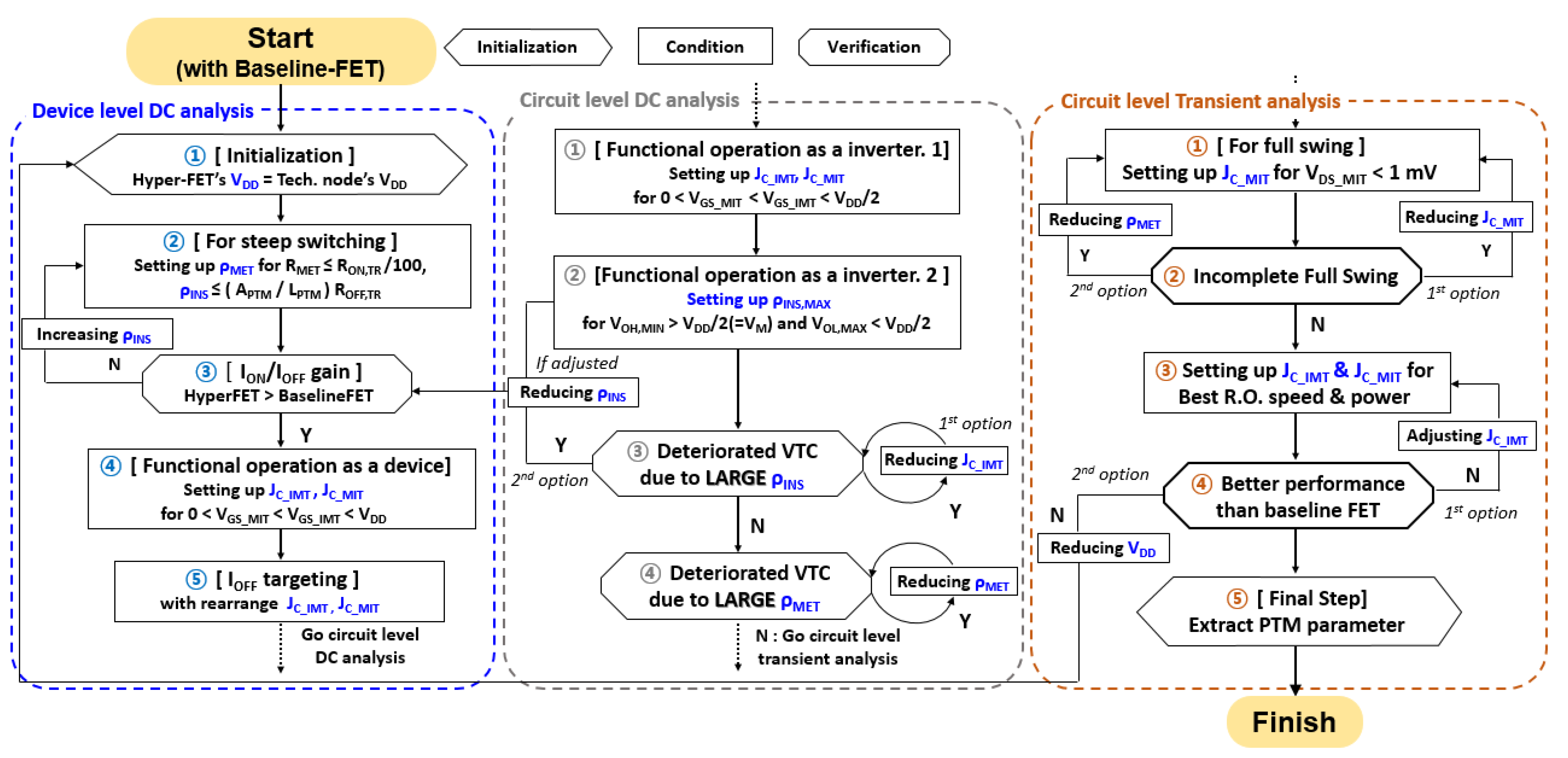
3.1. Hyper-FET Design Optimization Flow
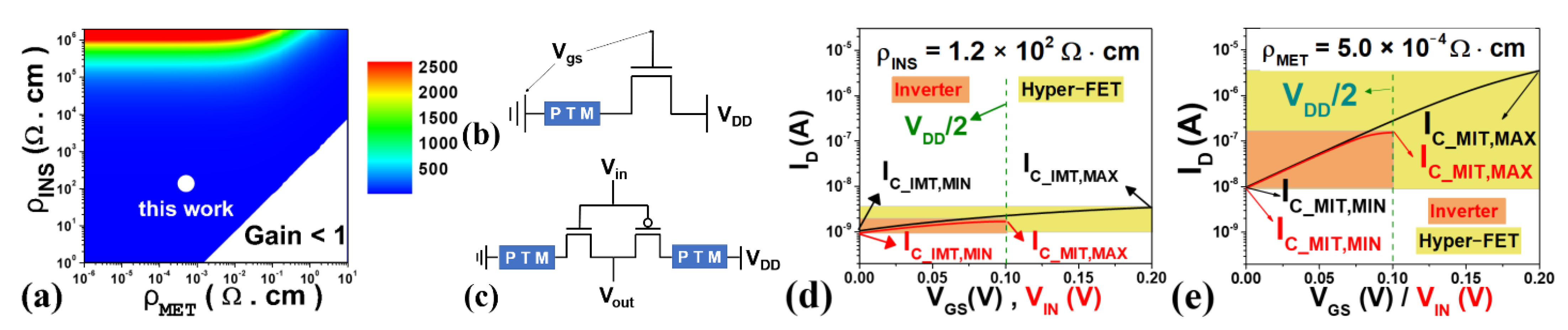
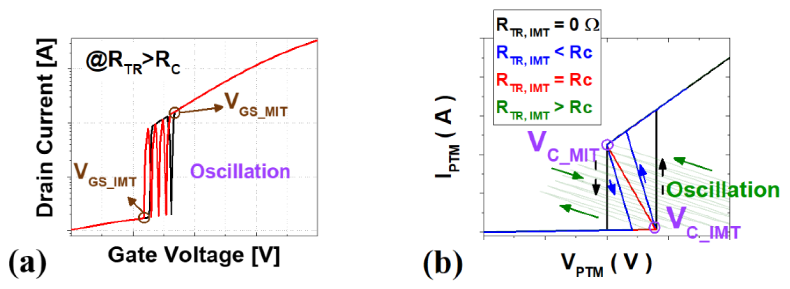
3.1.1. Device Level DC Analysis
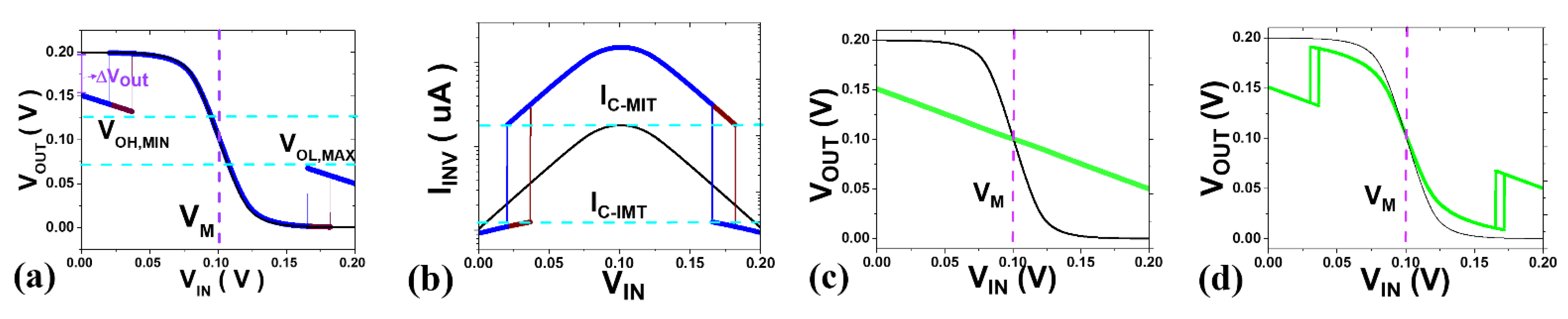
3.1.2. Circuit Level DC Analysis
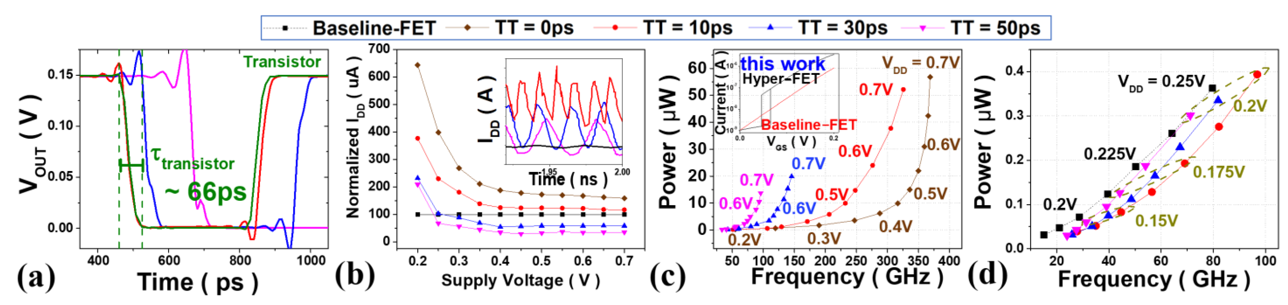
3.1.3. Circuit Level Transient Analysis
3.2. Benchmark with Conventional MOSFET Using INV RO
3.3. Benchmark with Conventional MOSFET Using 6T SRAM
4. Conclusions
Author Contributions
Funding
Data Availability Statement
Acknowledgments
Conflicts of Interest
References
- Yan, S.-C.; Wu, C.-H.; Sun, C.-J.; Lin, Y.-W.; Yao, Y.-J.; Wu, Y.-C. Trench FinFET Nanostructure with Advanced Ferroelectric Nanomaterial HfZrO2 for Sub-60-mV/Decade Subthreshold Slope for Low Power Application. Nanomaterials 2022, 12, 2165. [Google Scholar] [CrossRef] [PubMed]
- Azam, S.M.T.; Bakibillah, A.S.M.; Hasan, M.T.; Kamal, M.A.S. Effect of Step Gate Work Function on InGaAs p-TFET for Low Power Switching Applications. Nanomaterials 2021, 11, 3166. [Google Scholar] [CrossRef]
- Shukla, N.; Thathachary, A.V.; Agrawal, A.; Paik, H.; Aziz, A.; Schlom, D.G.; Summet, K.G.; Engel-Herbert, R.; Datta, S. A steep-slope transistor based on abrupt electronic phase transition. Nat. Commun. 2015, 6, 7812. [Google Scholar] [CrossRef] [PubMed] [Green Version]
- Zhang, Y.; Xiong, W.; Chen, W.; Zheng, Y. Recent progress on vanadium dioxide nanostructures and devices: Fabrication, properties, applications and perspectives. Nanomaterials 2021, 11, 338. [Google Scholar] [CrossRef] [PubMed]
- Song, B.; Cao, R.; Xu, H.; Liu, S.; Liu, H.; Li, Q. A HfO2/SiTe based dual-layer selector device with minor threshold voltage variation. Nanomaterials 2019, 9, 408. [Google Scholar] [CrossRef] [PubMed] [Green Version]
- Aziz, A.; Shukla, N.; Datta, S.; Gupta, S.K. Steep switching hybrid phase transition FETs (hyper-FET) for low power applications: A device-circuit co-design perspective—Part I. IEEE Trans. Electron Devices 2017, 64, 1350–1357. [Google Scholar] [CrossRef]
- Aziz, A.; Shukla, N.; Datta, S.; Gupta, S.K. Steep switching hybrid phase transition FETs (hyper-FET) for low power applications: A device-circuit co-design perspective—Part II. IEEE Trans. Electron Devices 2017, 64, 1358–1365. [Google Scholar] [CrossRef]
- International Roadmap for Devices and Systems (IRDS™). 2020. Available online: https://irds.ieee.org/editions/2020 (accessed on 23 July 2020).
- Ladd, L.A.; Paul, W. Optical and transport properties of high quality crystals of V2O4 near the metallic transition temperature. Solid State Commun. 1969, 7, 425–428. [Google Scholar] [CrossRef]
- Park, J.; Lee, D.; Yoo, J.; Hwang, H. NbO2 based threshold switch device with high operating temperature (>85 C) for steep-slope MOSFET (~2 mV/dec) with ultra-low voltage operation and improved delay time. In Proceedings of the 2017 IEEE International Electron Devices Meeting (IEDM), San Francisco, CA, USA, 2–6 December 2017; pp. 23–27. [Google Scholar]
- Yoo, J.; Kim, S.H.; Chekol, S.A.; Park, J.; Sung, C.; Song, J.; Donghwa, L.; Hwang, H. 3D stackable and scalable binary ovonic threshold switch devices with excellent thermal stability and low leakage current for high-density cross-point memory applications. Adv. Electron. Mater. 2019, 5, 1900196. [Google Scholar] [CrossRef]
- Sun, Y.; Zhao, X.; Song, C.; Xu, K.; Xi, Y.; Yin, J.; Wang, Z.; Zhou, X.; Chen, X.; Shi, G.; et al. Performance-enhancing selector via symmetrical multilayer design. Adv. Funct. Mater. 2019, 29, 1808376. [Google Scholar] [CrossRef]
- Jerry, M.; Shukla, N.; Paik, H.; Schlom, D.G.; Datta, S. Dynamics of electrically driven sub-nanosecond switching in vanadium dioxide. In Proceedings of the 2016 IEEE Silicon Nanoelectronics Workshop (SNW), Honolulu, HI, USA, 12–13 June 2016; pp. 26–27. [Google Scholar]
- Shukla, N.; Parihar, A.; Freeman, E.; Paik, H.; Stone, G.; Narayanan, V.; Wen, H.; Cai, Z.; Gopalan, V.; Engel-Herbert, R.; et al. Synchronized charge oscillations in correlated electron systems. Sci. Rep. 2014, 4, 4964. [Google Scholar] [CrossRef] [Green Version]
- Srinivasa, S.; Aziz, A.; Shukla, N.; Li, X.; Sampson, J.; Datta, S.; Kulkarni, J.P.; Narayana, V.; Gupta, S.K. Correlated material enhanced SRAMs with robust low power operation. IEEE Trans. Electron Devices 2016, 63, 4744–4752. [Google Scholar] [CrossRef]
- Mukherjee, D.; Mondal, H.K.; Reddy, B.V.R. Static noise margin analysis of SRAM cell for high speed application. Int. J. Comput. Sci. Issues (IJCSI) 2010, 7, 175. [Google Scholar]
- Wang, J.; Nalam, S.; Calhoun, B.H. Analyzing static and dynamic write margin for nanometer SRAMs. In Proceedings of the 13th International Symposium on Low Power Electronics and Design (ISLPED’08), Bangalore, India, 11–13 August 2008; pp. 129–134. [Google Scholar]


| Parameters | Values |
|---|---|
| Contacted poly-gate pitch (CPP) | 45 nm |
| Gate length (Lg) | 16 nm |
| Inner spacer thickness (Lsp) | 6 nm |
| Channel thickness (Tch) | 8 nm |
| Channel width (Wch) | 30 nm |
| Channel oxide thickness (Tox) | 0.3 nm |
| Channel high-k thickness (THK) | 1.1 nm |
| Bottom oxide thickness (TBO) | 20 nm |
| Channel doping | 1017 cm−3 |
| S/D doping | 3 × 102 cm−3 |
| PTS doping (upper of substrate 1) | 1 × 1019 cm−3 |
| Substrate 2 doping | 1017 cm−3 |
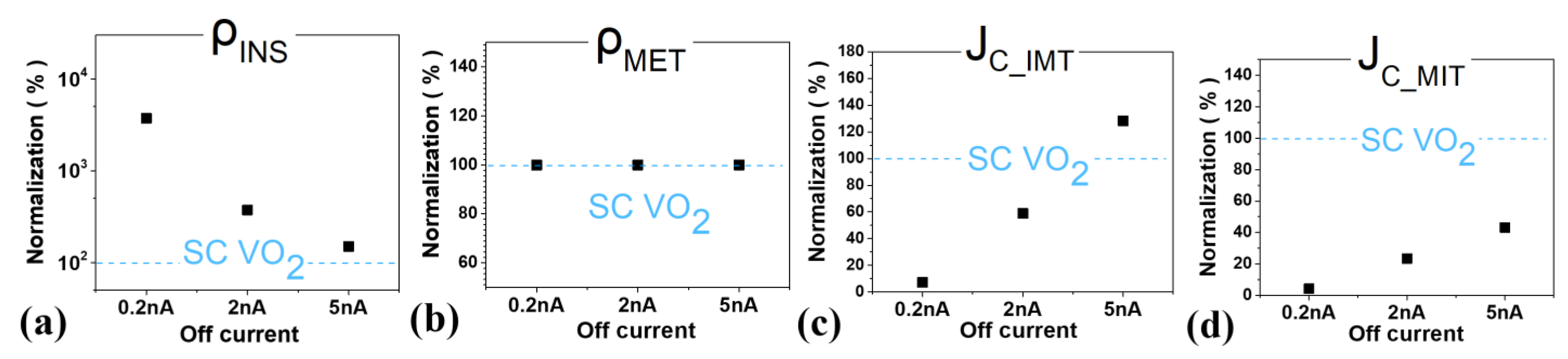
| Parameters | Value | |
|---|---|---|
| ρINS | Resistivity of Insulator state | 1.2 × 10² Ω·cm |
| ρMET | Resistivity of Metal state | 5.0 × 10⁻⁴ Ω·cm |
| JC_IMT | Critical Current Density for IMT | 2.4 × 10² A/cm2 |
| JC_MIT | Critical Current Density for MIT | 2.2 × 10³ A/cm2 |
| TT | PTM Switching Time | 50 ps |
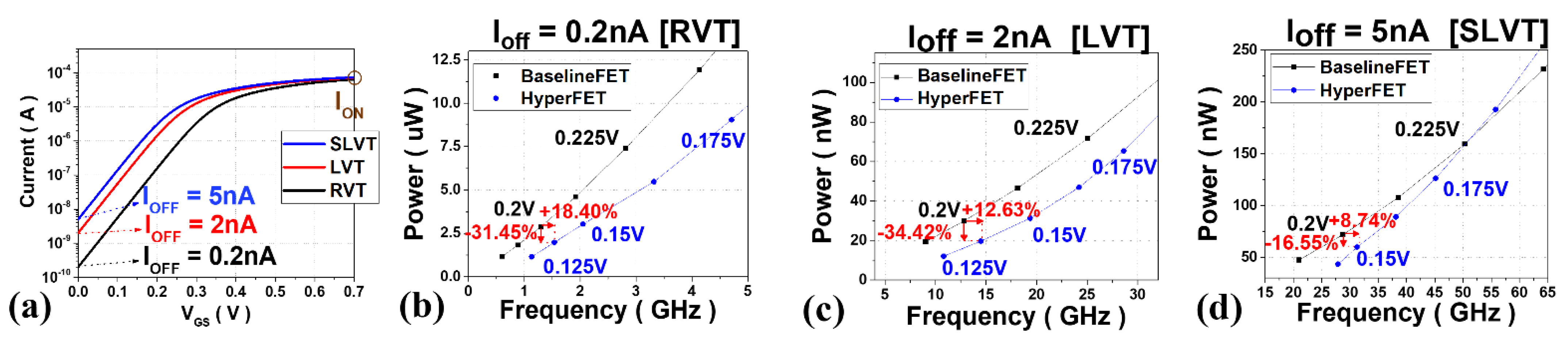
| IOFF = 5 nA | Baseline-FET (VDD = 0.2 V) | Hyper-FET | ||
|---|---|---|---|---|
| TT = 50 ps (VDD = 0.15 V) | TT = 30 ps (VDD = 0.1375 V) | TT = 10 ps (VDD = 0.1375 V) | ||
| Operating Frequency (GHz) | 2.87 × 101 (Ref.) | 3.13 × 101 (+8.96%) | 3.35 × 101 (+16.89%) | 3.50 × 101 (+21.83%) |
| Active Power (μW) | 7.18 × 10⁻² (Ref.) | 5.98 × 10⁻² (−16.68%) | 5.09 × 10⁻² (−29.10%) | 5.08 × 10⁻² (−29.24%) |
| TT = 50 ps | IOFF = 0.2 nA | IOFF = 2 nA | IOFF = 5 nA | |||
|---|---|---|---|---|---|---|
| Baseline-FET (VDD = 0.2 V) | Hyper-FET (VDD = 0.138 V) | Baseline-FET (VDD = 0.2 V) | Hyper-FET (VDD = 0.138 V) | Baseline-FET (VDD = 0.2 V) | Hyper-FET (VDD = 0.15 V) | |
| Operating Frequency (GHz) | 1.30 × 101 (Ref.) | 1.54 × 101 (+18.40%) | 1.29 × 101 (Ref.) | 1.45 × 101 (+12.63%) | 2.87 × 101 (Ref.) | 3.12 × 101 (+8.74%) |
| Active Power (μW) | 2.89 × 10⁻² (Ref.) | 1.98 × 10⁻² (−31.45%) | 3.00 × 10⁻² (Ref.) | 1.97 × 10⁻² (−34.42%) | 7.18 × 10⁻² (Ref.) | 5.99 × 10⁻² (−16.55%) |
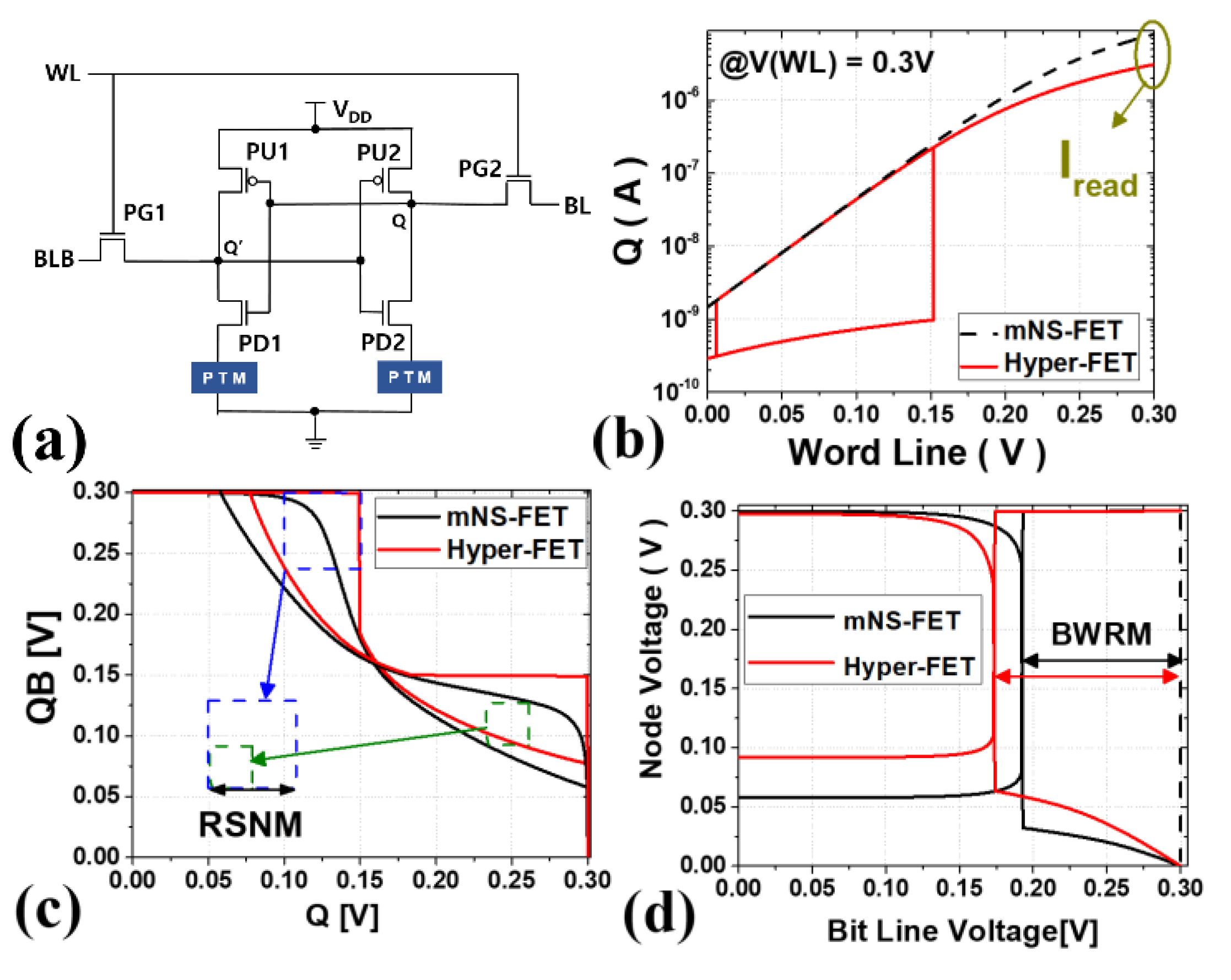
| Iread (μA) | RSNM (mV) | BWRM (mV) | Static Power (nW) | |
|---|---|---|---|---|
| mNS-FET 6T SRAM | 2.68 | 35.3 | 107.2 | 1.28 |
| Hyper-FET 6T SRAM | 1.57 | 50.8 | 117.3 | 0.53 |
| Improvement | −41.4% | +43.9% | +9.4% | +58.6% |
Publisher’s Note: MDPI stays neutral with regard to jurisdictional claims in published maps and institutional affiliations. |
© 2022 by the authors. Licensee MDPI, Basel, Switzerland. This article is an open access article distributed under the terms and conditions of the Creative Commons Attribution (CC BY) license (https://creativecommons.org/licenses/by/4.0/).
Share and Cite
Jung, H.; Chang, J.; Yoo, C.; Oh, J.; Choi, S.; Song, J.; Jeon, J. Hyper-FET’s Phase-Transition-Materials Design Guidelines for Ultra-Low Power Applications at 3 nm Technology Node. Nanomaterials 2022, 12, 4096. https://doi.org/10.3390/nano12224096
Jung H, Chang J, Yoo C, Oh J, Choi S, Song J, Jeon J. Hyper-FET’s Phase-Transition-Materials Design Guidelines for Ultra-Low Power Applications at 3 nm Technology Node. Nanomaterials. 2022; 12(22):4096. https://doi.org/10.3390/nano12224096
Chicago/Turabian StyleJung, Hanggyo, Jeesoo Chang, Changhyun Yoo, Jooyoung Oh, Sumin Choi, Juyeong Song, and Jongwook Jeon. 2022. "Hyper-FET’s Phase-Transition-Materials Design Guidelines for Ultra-Low Power Applications at 3 nm Technology Node" Nanomaterials 12, no. 22: 4096. https://doi.org/10.3390/nano12224096