Article

Device and Circuit Analysis of Double Gate Field Effect Transistor with Mono-Layer WS2-Channel at Sub-2 nm Technology Node

Department of Electrical and Electronics, Konkuk University, Seoul 05029, Korea
*
Author to whom correspondence should be addressed.
These authors contributed equally to this work.
Nanomaterials 2022, 12(13), 2299; https://doi.org/10.3390/nano12132299
Submission received: 18 May 2022 / Revised: 28 June 2022 / Accepted: 29 June 2022 / Published: 4 July 2022
(This article belongs to the Special Issue Nanotechnology for Electronic Materials and Devices)

Abstract

:
In this work, WS2 was adopted as a channel material among transition metal dichalcogenides (TMD) materials that have recently been in the spotlight, and the circuit power performance (power consumption, operating frequency) of the monolayer WS2 field-effect transistor with a double gate structure (DG WS2-FET) was analyzed. It was confirmed that the effective capacitance, which is circuit power performance, was greatly changed by the extrinsic capacitance components of DG WS2-FET, and the spacer region length (LSPC) and dielectric constant (KSPC) values of the spacer that could affect the extrinsic capacitance components were analyzed to identify the circuit power performance. As a result, when LSPC is increased by 1.5 nm with the typical spacer material (KSPC = 7.5), increased operating speed (+4.9%) and reduced active power (–6.8%) are expected. In addition, it is expected that the spacer material improvement by developing the low-k spacer from KSPC = 7.5 to KSPC = 2 at typical LSPC = 8 nm can increase the operating speed by 36.8% while maintaining similar active power consumption. Considering back-end-of-line (BEOL), the change in circuit power performance according to wire length was also analyzed. From these results, it can be seen that reducing the capacitance components of the extrinsic region is very important for improving the circuit power performance of the DG WS2-FET.

1. Introduction

Over the past few decades, semiconductor technology has made progress through scaling down and performance improvements of semiconductors according to Moore’s Law [1] and the Dennard scaling rule [2]. The planar MOSFET process was successfully replaced and commercialized because the so-called FinFET had better electrostatic control. This success of FinFET has led to the 5 nm technology node and is expected to reach beyond the technology node with the introduction of EUV [3,4]. Thanks to these structural changes and the success of FinFET through process optimization, the introduction of a gate-all-around (GAA) structure has recently been actively attempted in academia and industry. Among them, the nanosheet structure is in the spotlight as a strong candidate because it has gate controllability for channels superior to FinFET and more immunity for short channels [5,6,7]. It is expected that scaling due to such a structural change will have a limitation of less than or equal to 3 nm technology node, and a new channel material is attracting attention. Germanium and various III-V material-based channels have better carrier mobility than silicon channels and thus have better electrical properties [8,9]. Additionally, the channel application of two-dimensional materials is actively being studied [10]. Among them, it is noted that a TMD material is thin and thus may effectively reduce a short channel effect and replace silicon due to its excellent interface characteristics and excellent mobility characteristics due to an absence of dangling bond due to Van der Waals bonding [11,12]. In addition, the results of device characteristic analysis through process developments such as contact resistance and doping technology and atomic level analysis have recently been announced [13]. In addition, recently, research on TMD materials has been actively conducted, and research on a FinFET device in which a single-layer TMD material is vertically aligned has been conducted [14,15,16,17,18]. Recently, Z.Ahmed presented DG FET with mono-layer WS2 channels and device and circuit power performance that multi-stacked them, showing the possibility of using TMD in sub-2 nm technology node [19]. In this work, the quantitatively analyzed effect of extrinsic components of DG WS2-FET on circuit power performance to optimize circuit power performance based on these research results was performed, and a device design guideline for scaling down to improve circuit performance based on DG WS2-FET is presented. In addition, the changes in circuit power performance according to various circuit layout types were analyzed.
In this work, based on the DG WS2-FET proposed by Z.Ahmed [19], a circuit model library was developed, and device and circuit co-analysis was performed. Through this, the effect of front-end-of-line (FEOL), middle-of-line (MOL), and BEOL on the circuit in DG WS2-FET technology is analyzed, and optimization through changes in the performance of the circuit by various KSPC and contacted gate pitch (CGP) by spacer length is analyzed (CGP = LCH + LCNT + 2 LSPC). Through this, we present a circuit process development guide for TMD materials that are spotlighted as next-generation materials beyond silicon.

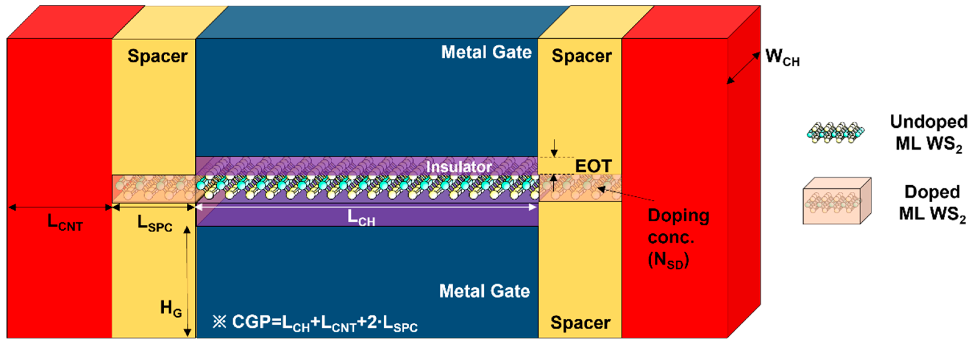
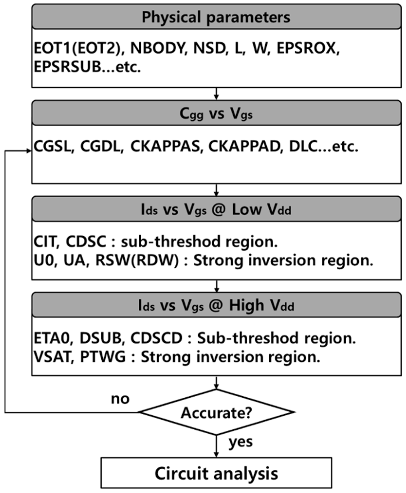
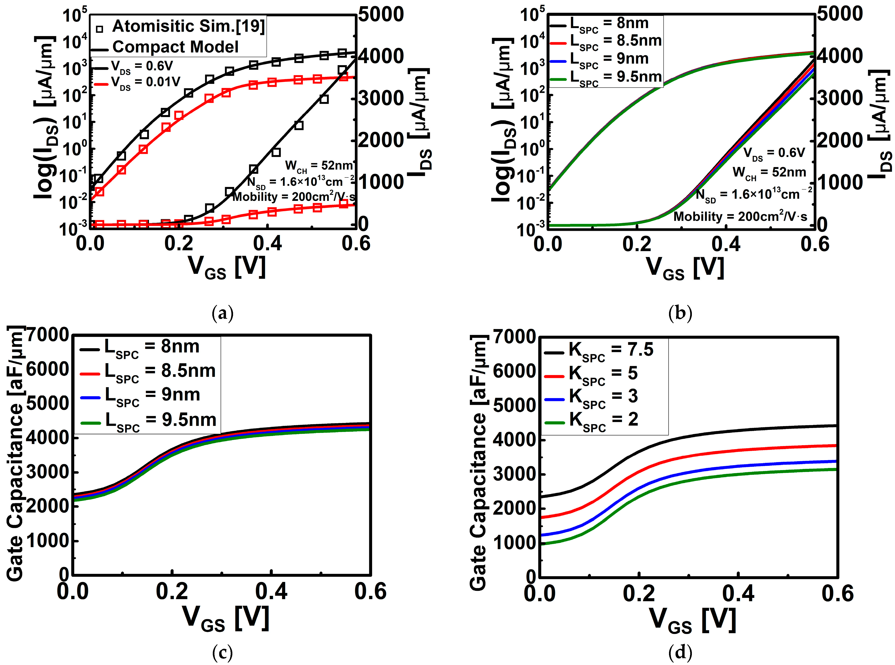
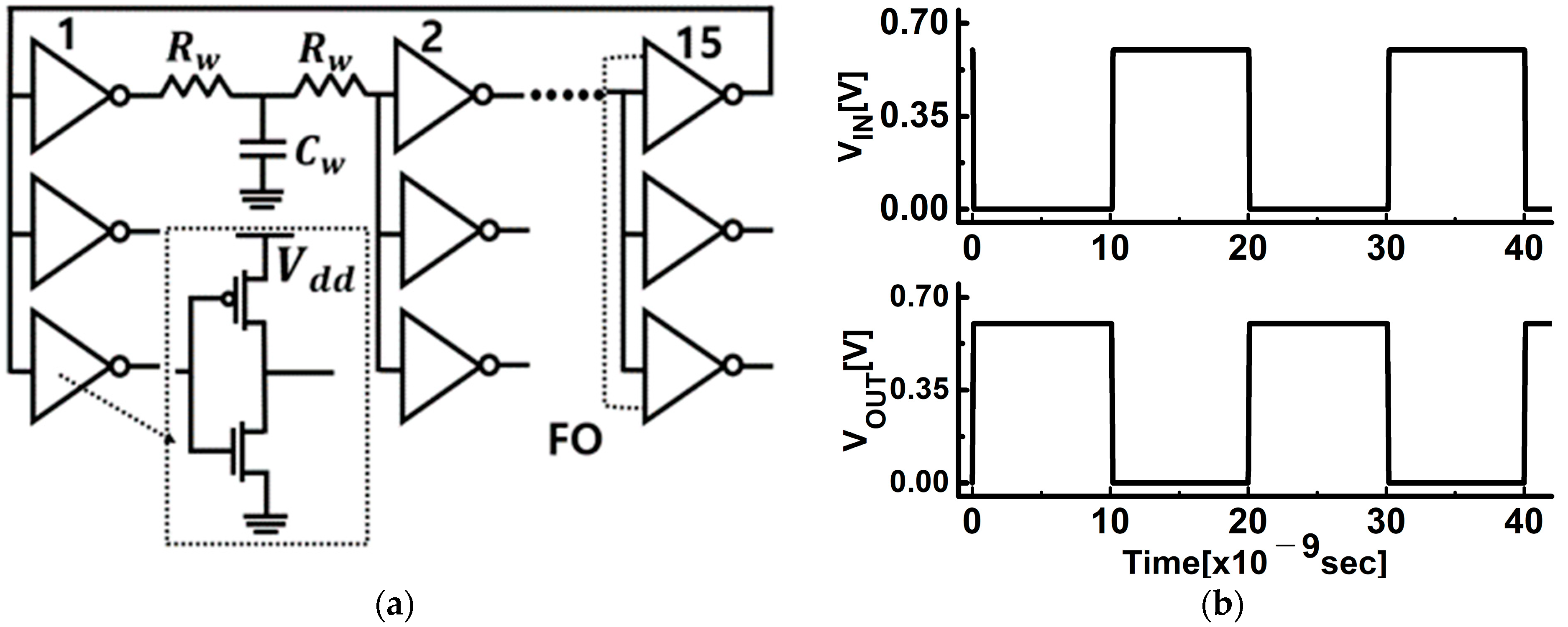
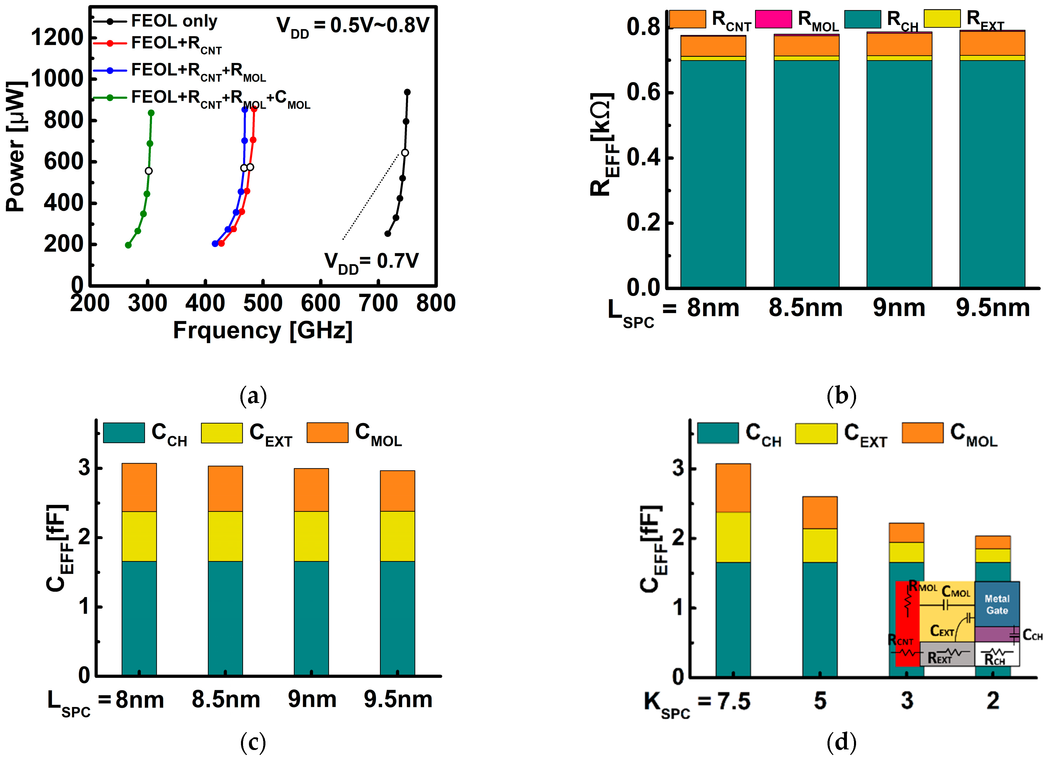
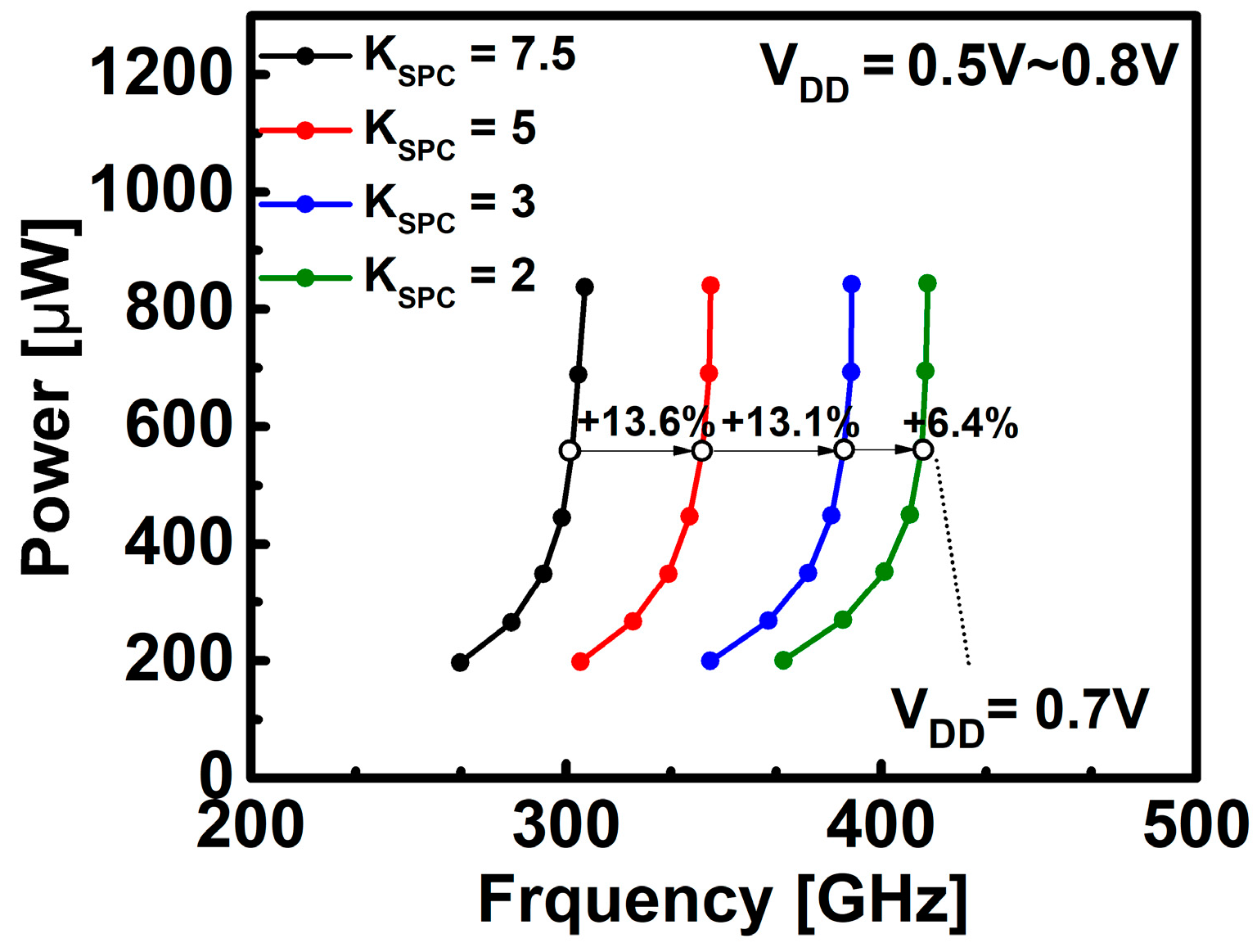
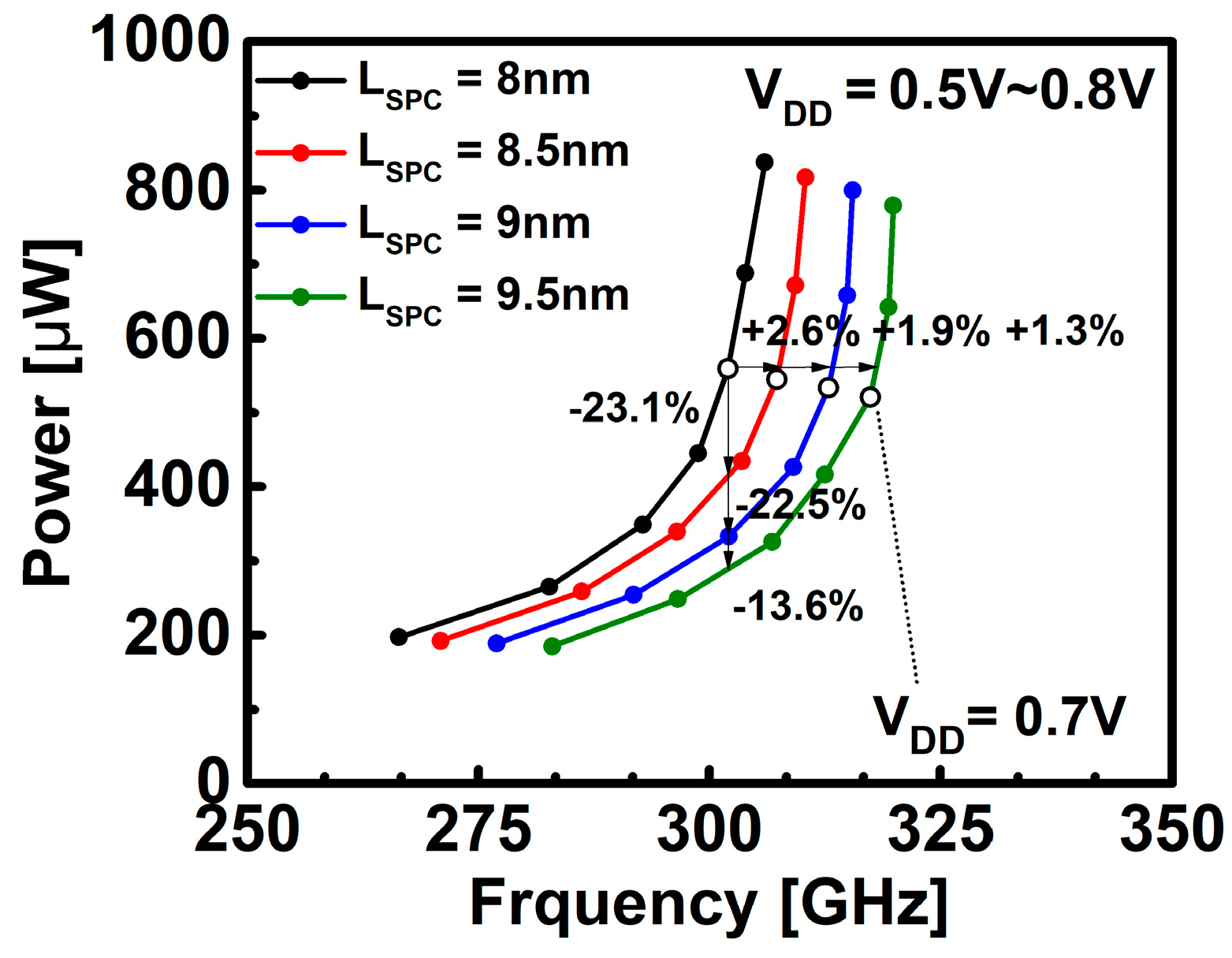
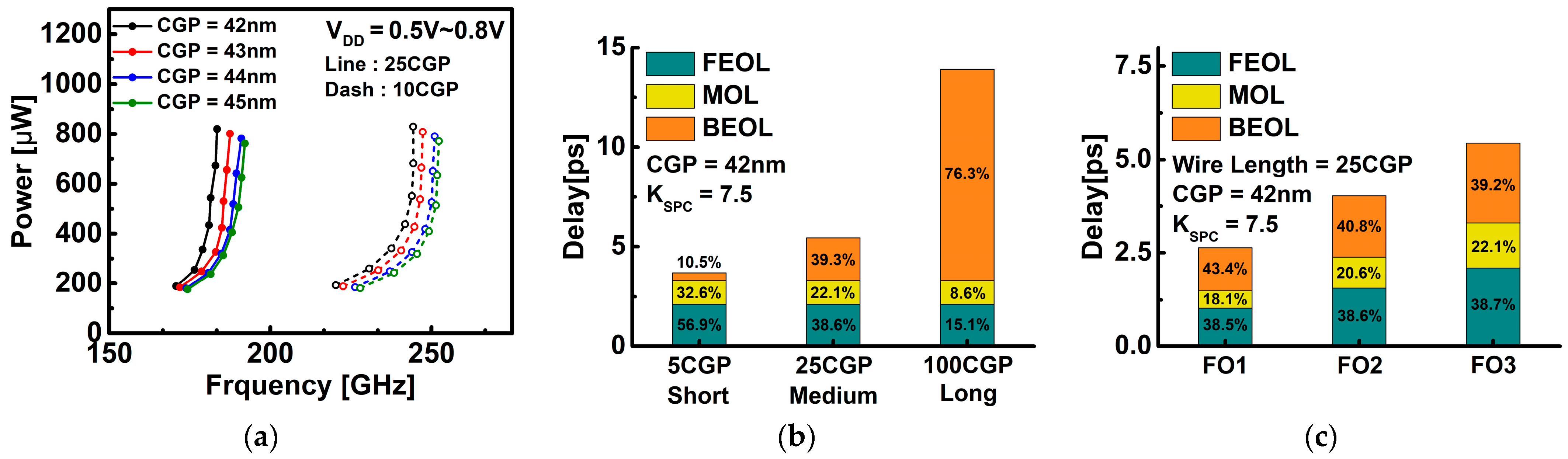
2. Device and Circuit Co-Analysis of DG WS2-FET

The scaling-down technology based on the CGP and metal pitch (MP) becomes the core of the semiconductor scaling technology, enabling low power and high operating speed. However, silicon technology is facing limitations, and TMD continues to scale down beyond its limitations due to its material characteristics. Figure 1 shows the DG WS2-FET used in this work. Based on the CGP for the 2 nm technology node [19], CGP by various spacer lengths is presented and summarized as a physical parameter in Table 1. The source/drain extension region below the spacer was considered a heavily doped region with a carrier density (NSD) of 1.6 × 1013 cm2, and the resistance of the extension region is 16 Ω∙μm.
The electrical properties of DG WS2-FET were obtained using atomistic analysis and the calibrated commercial TCAD simulator. The calibration process of DG WS2-FET in Figure 1 was performed using the I-V transfer curve based on the atomistic level simulation of Ref. [19], and through this process, the C-V characteristic curve was obtained to secure the electrical characteristics of DG WS2-FET. Note that an effective mobility (= 200 cm2/V∙s) of the monolayer WS2 channel was estimated in previous work [19] through atomistic calculation, and we take this value in I-V characteristics. Based on the obtained I-V and C-V data, circuit model library generation was performed by using BSIM-IMG [20]. Figure 2 shows the overall BSIM-IMG model parameter extraction flow used in this work. Figure 3a is I-V transfer curve that can confirm the consistency of reference device simulation and performed circuit simulation. The off current (IOFF) was the current flowing through the channel when VGS = 0 V and VDS = 0.6 V (supply voltage), and it was targeted at 2 nA. Figure 3b,c are the drain current change and gate capacitance change according to the change of LSPC, respectively. As shown in Figure 3b, when the LSPC increases, the current of the DG WS2-FET decreases because of the resistance component in the extension.
Region (REXT) increases. This phenomenon is the same as the general phenomenon that appears in devices such as silicon FinFET [21]. However, although the ION/IOFF ratio and subthreshold swing (SS) are noticeably changed in silicon FinFET, there is little ION/IOFF ratio and SS change because the LSPC change is very small in this work (in all cases of LSPC = 8 nm ~ 9.5 nm of DG WS2-FET, the ION/IOFF ratio is about 1.33 × 10⁵, and SS is about 69 mV/dec). As LSPC increases in Figure 3c, the gate capacitance decreases because the capacitance component by the gate fringe field (CEXT) and the capacitance component between the gate and MOL contact (CMOL) are affected by the LSPC. That is, it can be seen that LSPC is a key parameter that scales REXT and CMOL, which are parasitic components excluding the intrinsic components of the device. In addition, it can be expected that there will be a change in the extrinsic component not only in the LSPC but also in the change in the spacer material. Therefore, the influence of the lower dielectric constant of the spacer (KSPC) was also investigated. As shown in Figure 3d, the gate capacitance is significantly reduced by reducing KSPC as CEXT and CMOL are reduced by the influence of KSPC.
The circuit simulator and circuit scheme used in this work are Synopsys’ HSPICE and inverter ring-oscillator with fan-out = 3 (FO3 INV RO), respectively, which are widely used in the industry. The FO3 INV RO circuit is depicted in Figure 4a and consists of 15 stages. The R/C component of the BEOL load was attached between the output of one inverter and the input of the next stage. From the INV RO circuit simulation results as shown in Figure 4b, the average signal delay can be extracted to obtain a frequency representing the speed of the operation, and the active dynamic power at the same static power can be extracted.
Figure 5a illustrates the change in circuit power performance when considering contact resistance (RCNT) and MOL R/C components (RMOL,CMOL) with intrinsic channel. A contact resistance of 80 Ω∙μm, the target value of Ref. [19], was adopted. In the developed circuit model, RCNT, RMOL, and CMOL were considered by attaching these components to both ends of the source and drain of BSIM-IMG model for the DG WS2-FET. Based on VDD (supply voltage) = 0.7 V, when RCNT was considered under the same power condition, the operation frequency was decreased by 35.6%, and in addition, considering RMOL, it was confirmed that there was a decrease of 2.6%, and when CMOL is added, it is decreased by 35.1%.
The elements that determine the circuit operation characteristics were analyzed using the segmentation technique. This is possible by extracting the operating frequency, the IDDA (active current), and the IDDQ (leakage current) from the inverter ring oscillator circuit.
The operating behavior, and the calculating effective resistance (REFF) and capacitance (CEFF), represent the circuit operating speed and power consumption [22]. The circuit characteristics were analyzed by adjusting the WS2 channel, contact resistance, and MOL of the circuit model during circuit simulation, and the effects of each component were observed in REFF and CEFF.
The RCH characteristics that vary with the gate voltage of the device are all reflected in the REFF obtained from the simulation, including the dynamic behavior characteristics of the circuit, which are shown in Figure 5b. The ratio in which the channel and the extension region form the resistance was extracted from VDS = 0.6 V and VGS = 0.6 V under the condition that only FEOL is considered. In Figure 5b, it can be seen that as the LSPC becomes larger, the REFF also increases. In particular, the effect of the channel, the contact resistance, and the MOL resistance on circuits is almost constant, even if LSPC changes, and it can be seen that REXT increases. REXT increased by about 24% as LSPC increased from 8 nm to 9.5 nm. This fact can be explained in Figure 3b as the LSPC increases and the current decreases. In Figure 5c, it can be observed that as LSPC increases, CMOL mainly decreases and the total CEFF decreases. It can be seen from Figure 5d that the CEFF decreases as the KSPC decreases. CEXT and CMOL can be called the parasitic capacitance components, and as the KSPC decreases, it can be seen that the CEXT and CMOL gradually decrease. Through Figure 5b–d, the REFF can be improved through LSPC scaling, and the importance of the CEFF can be understood through the change of the spacer material.
Figure 6 and Figure 7 show the results of inverter ring oscillator circuit simulation according to the changes in KSPC and LSPC. Figure 6 shows that the operating frequency is improved by 13% to 37% at VDD = 0.7 V based on the default KSPC (=7.5). As confirmed in Figure 5c, the operating speed of the circuit was improved through the reduction of the capacitance by the KSPC.
As a result of Figure 7, which shows that the performance increases as the LSPC increases, it can be seen that even if the REXT increases and the overall resistance increases, the performance is improved due to the capacitance component reduced by the LSPC. At VDD = 0.7 V, the frequency increases by 2% to 5% and the power decreases by 3% to 7% based on the default LSPC (=8 nm). Since the increased LSPC from the point of view of area scaling is not positive, the improvement of the KSPC is more effective.
Through Figure 8, the effect of the wiring length and BEOL load on the circuit can be analyzed. The wire resistance of the BEOL load was applied as RW = 1447 Ω/μm, and the wire capacitance was applied as CW = 208 aF/μm [23]. As the LSPC changes from 8 nm to 9.5 nm, the CGP changes from 42 nm to 45 nm. Figure 8a shows a power-frequency curve by a BEOL interconnect according to two wiring lengths of 25 CGP and 10 CGP. In each CGP case, it can be seen that the speed change according to the wiring length is 32% to 34%, and the effect of the BEOL component on the circuit is significant. In Figure 8b, the effect of the BEOL load on delay was analyzed by dividing the wiring length into 5 CGP, 25 CGP, and 100 CGP, into short, medium, and long cases, respectively. Based on 25 CGP, the delay decreased by 32% at 5 CGP, and at 100 CGP, the delay increased by 2.5 times. Figure 8c is an analysis of the delay of the circuit according to fan-out dependency when considering the BEOL load. As the fan-out number increases and the total number of inverters in the circuit increases, the delay increases. In addition, it can be seen that not only the delay by the fan-out number increases but also the delay by each component (FEOL, MOL, and BEOL) increases. Figure 8 shows that while the FEOL and MOL processes are of course important, the performance improvements through the BEOL process optimization are essential.

3. Conclusions

This work analyzes the effect of performance change through LSPC scaling and KSPC change and the FEOL, MOL, and BEOL components of TMDC FET technology on the circuit based on the previous work using the WS2 channel transistor of the double gate structure. In particular, it was confirmed that increasing LSPC is more beneficial to circuit power performance, but there is a trade-off from the viewpoint of area, and it was also seen that the change in KSPC has a great influence on speed improvement. This work confirmed that BEOL optimization is very important, as well as FEOL and MOL, through the effect of the BEOL load by various CGP cases and wiring lengths and the fan-out number on the circuit.

Author Contributions

J.P. and C.R. contributed to the main idea and writing of this research. J.L. performed the ring oscillator simulations. This research was planned and executed under the supervision of J.J. All authors have read and agreed to the published version of the manuscript.

Funding

This work was supported the National Foundation of Korea (NRF) grant funded by the Korea government (MIST) (No.2020M3F3A2A01081595) and partly by the National Foundation of Korea (NRF) grant funded by the Korea government (MIST) (No.2020M3F3A2A01082326).

Institutional Review Board Statement

Not applicable.

Data Availability Statement

Not applicable.

Acknowledgments

The EDA tool was supported by the IC Design Education Center (IDEC), Korea.

Conflicts of Interest

The authors declare no conflict of interest.

References

  1. Moore, G. Cramming More Components Onto Integrated Circuits. Proc. IEEE 1998, 86, 82–85. [Google Scholar] [CrossRef]
  2. Dennard, R.H.; Gaensslen, F.H.; Yu, H.; Rideout, V.L.; Bassous, E.; LeBlanc, A.R. Design of ion-implanted MOSFET’s with very small physical dimensions. IEEE Solid-State Circuits Soc. Newsl. 2007, 12, 38–50. [Google Scholar] [CrossRef]
  3. Colinge, J.P. (Ed.) FinFETs and Other Multi-Gate Transistors; Springer: New York, NY, USA, 2008. [Google Scholar]
  4. Xie, R.; Montanini, P.; Akarvardar, K.; Tripathi, N.; Haran, B.; Johnson, S.; Hook, T.; Hamieh, B.; Corliss, D.; Wang, J.; et al. A 7nm FinFET Technology Featuring EUV Patterning and dual strained high mobility channels. In Proceedings of the 2016 IEEE International Electron Devices Meeting (IEDM), San Francisco, CA, USA, 3–7 December 2016; pp. 1–4. [Google Scholar]
  5. Lee, Y.; Park, G.-H.; Choi, B.; Yoon, J.; Kim, H.-J.; Kim, D.H.; Kim, D.M.; Kang, M.-H.; Choi, S.-J. Design study of the gate-all-around silicon nanosheet MOSFETs. Semicond. Sci. Technol. 2020, 35, 03LT01. [Google Scholar] [CrossRef]
  6. Jang, D.; Yakimets, D.; Eneman, G.; Schuddinck, P.; Bardon, M.G.; Raghavan, P.; Spessot, A.; Verkest, D.; Mocuta, A. Device exploration of nanosheet transistors for sub-7-nm technology node. IEEE Trans. Electron. Devices 2017, 64, 2707–2713. [Google Scholar] [CrossRef]
  7. Thomas, S. Gate-all-around transistors stack up. Nat. Electron. 2020, 3, 728. [Google Scholar] [CrossRef]
  8. Yeo, Y.-C.; Gong, X.; van Dal, M.J.H.; Vellianitis, G.; Passlack, M. Germanium-based transistors for future high performance and low power logic applications. In Proceedings of the 2015 IEEE International Electron Devices Meeting (IEDM), Washington, DC, USA, 7–9 December 2015; pp. 1–4. [Google Scholar]
  9. Chen, Y.; Liu, J.; Zeng, M.; Lu, F.; Lv, T.; Chang, Y.; Lan, H.; Wei, B.; Sun, R.; Gao, J.; et al. Universal growth of ultra-thin III–V semiconductor single crystals. Nat. Commun. 2020, 11, 3979. [Google Scholar] [CrossRef] [PubMed]
  10. Chhowalla, M.; Jena, D.; Zhang, H. Two-dimensional semiconductors for transistors. Nat. Rev. Mater. 2016, 1, 16052. [Google Scholar] [CrossRef]
  11. Agarwal, T.; Yakimets, D.; Raghavan, P.; Radu, I.; Thean, A.; Heyns, M.; Dehaene, W. Benchmarking of MoS2FETs With Multigate Si-FET Options for 5 nm and Beyond. IEEE Trans. Electron. Devices 2015, 62, 4051–4056. [Google Scholar] [CrossRef]
  12. Rai, A.; Movva, H.C.P.; Roy, A.; Taneja, D.; Chowdhury, S.; Banerjee, S.K. Progress in Contact, Doping and Mobility Engineering of MoS2: An Atomically Thin 2D Semiconductor. Crystals 2018, 8, 316. [Google Scholar] [CrossRef] [Green Version]
  13. Shen, P.-C.; Su, C.; Lin, Y.; Chou, A.-S.; Cheng, C.-C.; Park, J.-H.; Chiu, M.-H.; Lu, A.-Y.; Tang, H.-L.; Tavakoli, M.M.; et al. Ultralow contact resistance between semimetal and monolayer semiconductors. Nature 2021, 593, 211–217. [Google Scholar] [CrossRef] [PubMed]
  14. Chen, M.-L.; Sun, X.; Liu, H.; Wang, H.; Zhu, Q.; Wang, S.; Du, H.; Dong, B.; Zhang, J.; Sun, Y.; et al. A FinFET with one atomic layer channel. Nat. Commun. 2020, 11, 1205. [Google Scholar] [CrossRef] [PubMed] [Green Version]
  15. Afzalian, A. Ab initio perspective of ultra-scaled CMOS from 2D-material fundamentals to dynamically doped transistors. npj 2D Mater. Appl. 2021, 5, 5. [Google Scholar] [CrossRef]
  16. Mitta, S.B.; Choi, M.S.; Nipane, A.; Ali, F.; Kim, C.; Teherani, J.T.; Hone, J.; Yoo, W.J. Electrical characterization of 2D materials-based field-effect transistors. 2D Mater. 2020, 8, 012002. [Google Scholar] [CrossRef]
  17. Sebastian, A.; Pendurthi, R.; Choudhury, T.H.; Redwing, J.M.; Das, S. Benchmarking monolayer MoS2 and WS2 field-effect transistors. Nat. Commun. 2021, 12, 693. [Google Scholar] [CrossRef] [PubMed]
  18. Arutchelvan, G.; Smets, Q.; Verreck, D.; Ahmed, Z.; Gaur, A.; Sutar, S.; Jussot, J.; Groven, B.; Heyns, M.; Lin, D.; et al. Impact of device scaling on the electrical properties of MoS2 field-effect transistors. Sci. Rep. 2021, 12, 6610. [Google Scholar] [CrossRef] [PubMed]
  19. Ahmed, Z.; Afzalian, A.; Schram, T.; Jang, D.; Verreck, D.; Smets, Q.; Schuddinck, P.; Chehab, B.; Sutar, S.; Arutchelvan, G.; et al. Introducing 2D-FETs in Device Scaling Roadmap using DTCO. In Proceedings of the 2020 IEEE International Electron Devices Meeting (IEDM), San Francisco, CA, USA, 12–18 December 2020; pp. 1–4. [Google Scholar]
  20. Hu, C.; Niknejad, A.; Sriramkumar, V.; Lu, D.; Chauhan, Y.; Kahm, M.; Sachid, A. BSIM-IMG: A Turnkey compact model for fully depleted technologies. In Proceedings of the 2012 IEEE International SOI Conference (SOI), Napa, CA, USA, 1–4 October 2012; pp. 1–24. [Google Scholar]
  21. Park, J.; Kim, J.; Showdhury, S.; Shin, C.; Rhee, H.; Yeo, M.; Cho, E.-C.; Yi, J. Electrical Characteristics of Bulk FinFET According to Spacer Length. Electronics 2020, 9, 1283. [Google Scholar] [CrossRef]
  22. Yu, X.; Han, S.; Zamdmer, N.; Deng, J.; Nowak, E.J.; Rim, K. Improved effective switching current (IEFF+) and capacitance methodology for CMOS circuit performance prediction and model-to-hardware correlation. In Proceedings of the 2008 IEEE International Electron Devices Meeting, San Francisco, CA, USA, 15–17 December 2008; pp. 1–4. [Google Scholar]
  23. International Roadmap for Devices and Systems (IRDS™). 2020. Available online: https://irds.ieee.org/editions/2020 (accessed on 23 July 2020).
Figure 1. Structure of DG WS2-FET used in this work.
Nanomaterials 12 02299 g001
Figure 2. BSIM-IMG model parameter extraction flow used in this work.
Nanomaterials 12 02299 g002
Figure 3. (a) I−V transfer curve of DG WS2-FET. The black line is when high voltage (VDS = 0.6 V) is applied, and the red line is when the low voltage (VDS = 0.01 V) is applied; (b) I−V transfer curve according to LSPC when high voltage applied; (c) gate capacitance according to LSPC; and (d) gate capacitance according to KSPC.
Nanomaterials 12 02299 g003
Figure 4. (a) Schematic of inverter ring oscillator with fan−out 3, which includes distributed interconnect RC components; (b) the transient simulation results of designed inverter ring oscillator.
Nanomaterials 12 02299 g004
Figure 5. (a) Circuit power performance (power consumption, operating frequency) when contact resistance and MOL components are added to the intrinsic channel; (b) analysis of results of the effect of various components on circuit using REFF; (c) analysis of results of the effect of various components on circuit according to LSPC using CEFF; (d) analysis of results of the effect of various components on circuit according to KSPC using CEFF. The figure inserted in (d) shows resistances for channel (RCH), extension (REXT), contact (RCNT), and MOL (RMOL) and capacitances for channel (CCH), extension (CEXT), and MOL (CMOL), respectively.
Nanomaterials 12 02299 g005
Figure 6. Power versus frequency for DG WS2-FET according to KSPC.
Nanomaterials 12 02299 g006
Figure 7. Power versus frequency for DG WS2-FET according to LSPC.
Nanomaterials 12 02299 g007
Figure 8. (a) Power versus frequency for DG WS2-FET according to CGP due to changes in LSPC with BEOL load (KSPC = 7.5). The wire length is 25 CGP, 10 CGP. (b) Analysis of delay of designed inverter ring oscillator with BEOL load. The wire length was considered in three cases (5 CGP, 25 CGP, and 100 CGP) in the BEOL load. (c) Analysis of delay of designed inverter ring oscillator with BEOL considering fan-out dependency.
Nanomaterials 12 02299 g008
Table 1. Key device geometric parameters of DG WS2-FET.
Geometric Parameter
CGP (nm)42434445
LSPC (nm)88.599.5
LG (nm)14141414
MP (nm)16161616
LCNT (nm)12121212
EOT (nm)0.50.50.50.5
WCH (nm)52525252
HG (nm)20202020
WCH: width of the channel of DG WS2-FET.
Publisher’s Note: MDPI stays neutral with regard to jurisdictional claims in published maps and institutional affiliations.

