
Conducting Interface for Efficient Growth of Vertically Aligned Carbon Nanotubes: Towards Nano-Engineered Carbon Composite


Abstract
:1. Introduction
1.1. Importance of Carbon Nanotubes (CNT) in the Development of Innovative Materials
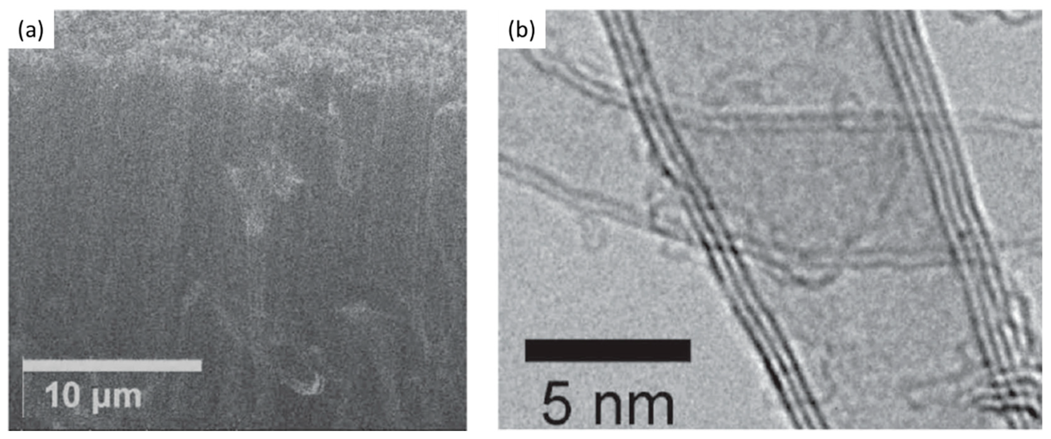
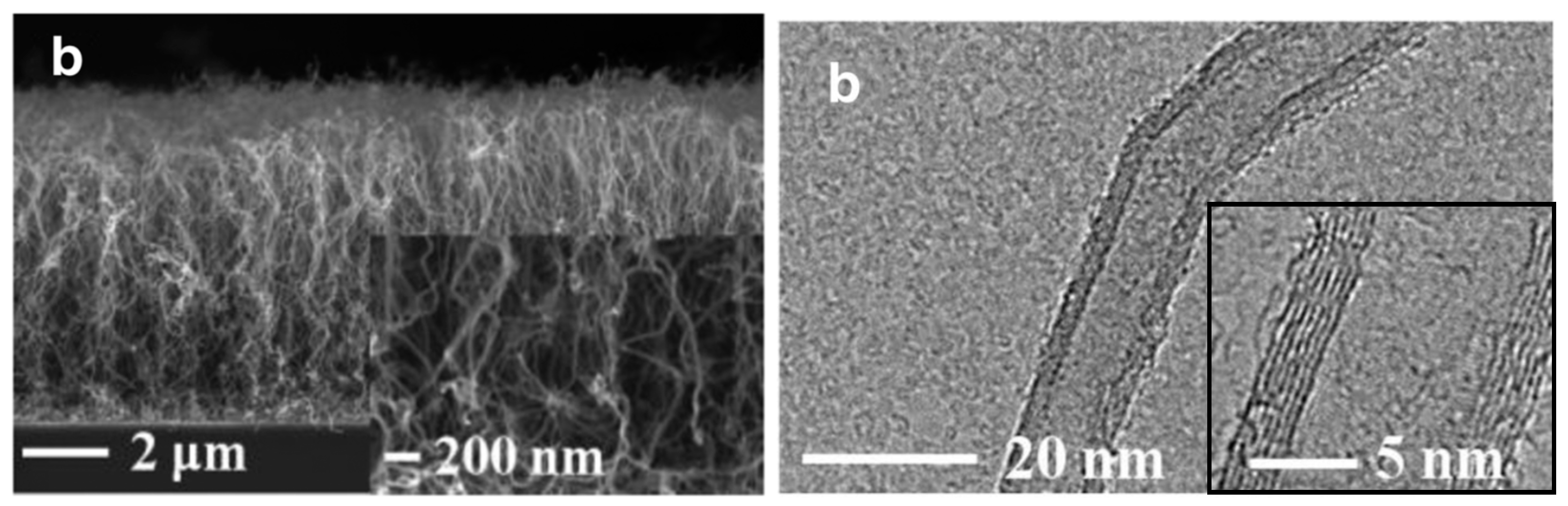
1.2. Vertically Aligned Carbon Nanotubes (VACNT)—CNT Assembly with Specific Advanced Properties
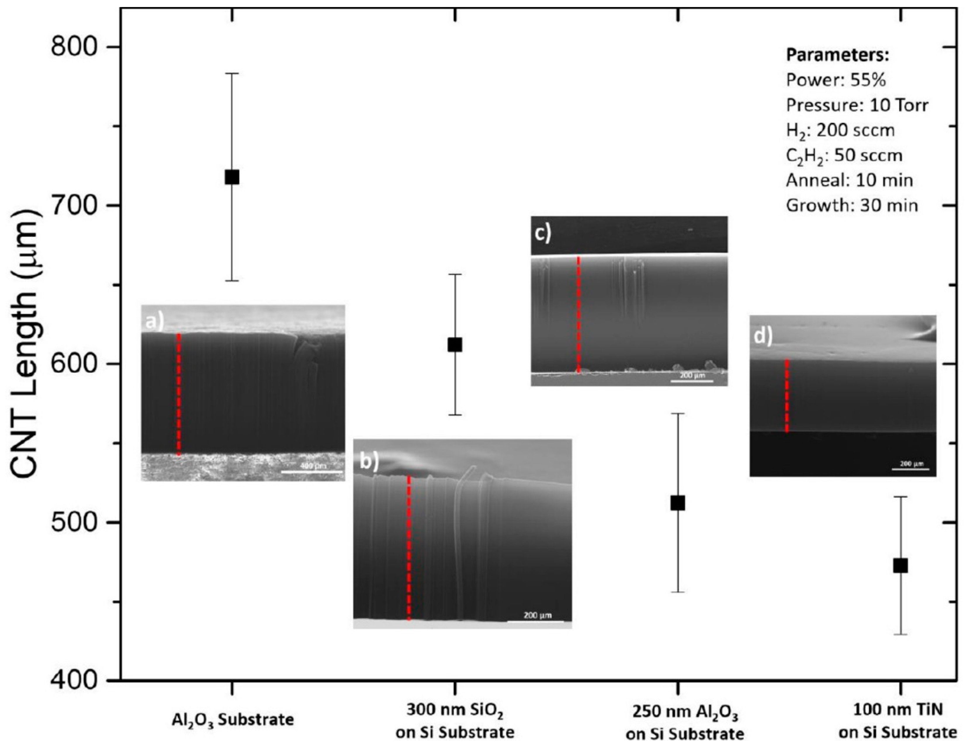
1.3. Substrates for Growth of VACNT
1.4. DBL towards Enhanced Growth of VACNT on Diverse Flat and 3-D Fibrous Substrates
2. Conducting DBL Solution for the Growth of VACNT on Flat and 3-D Fibrous Substrates
2.1. Via Chemical Vapour Deposition (CVD)
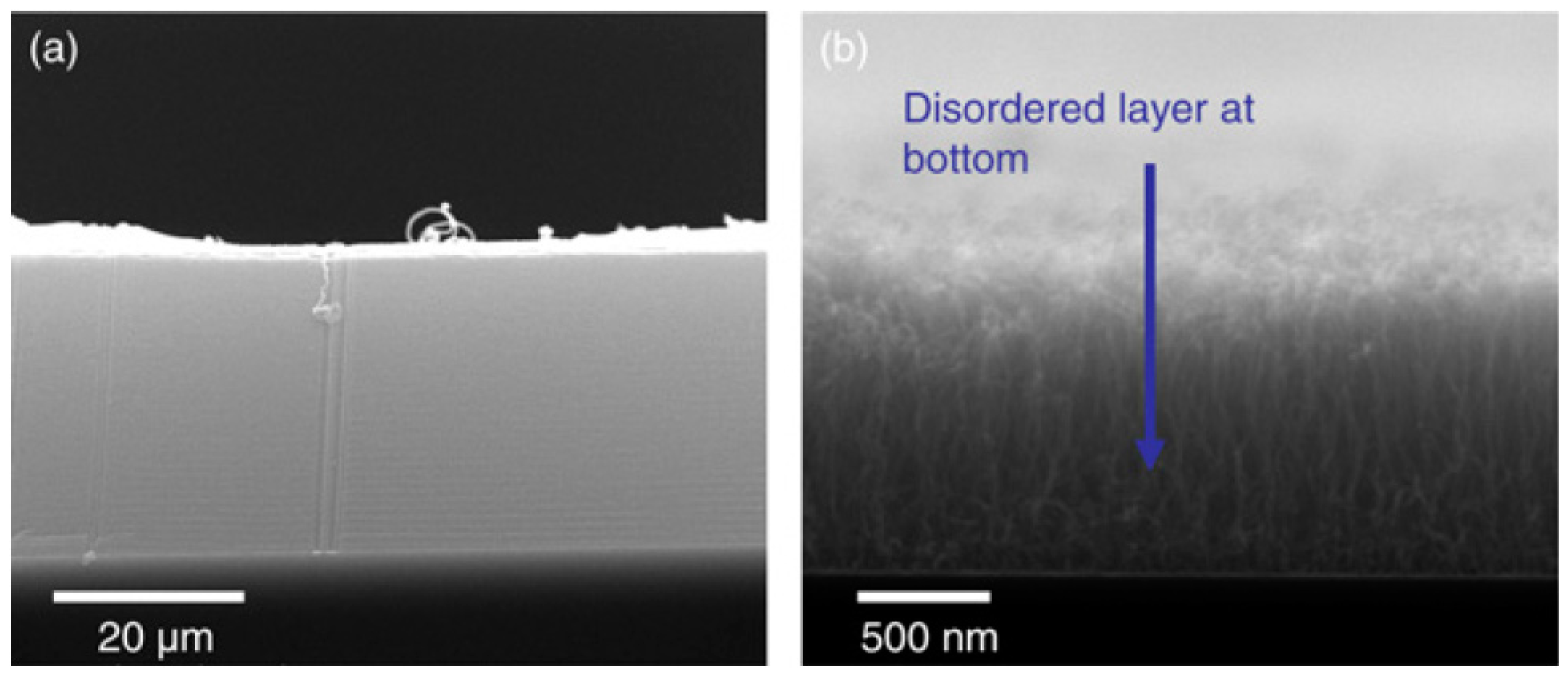
2.2. Via Physical Vapour Deposition (PVD)
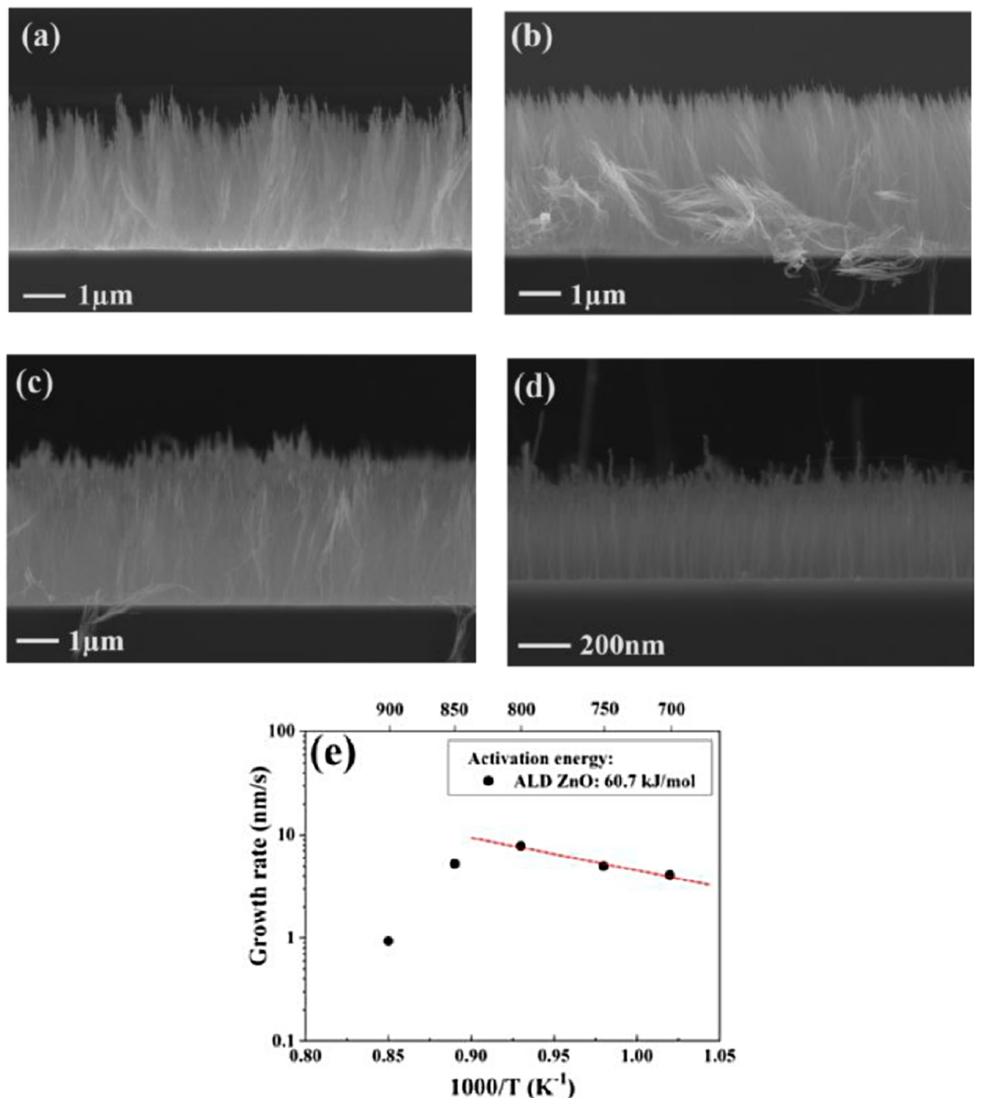
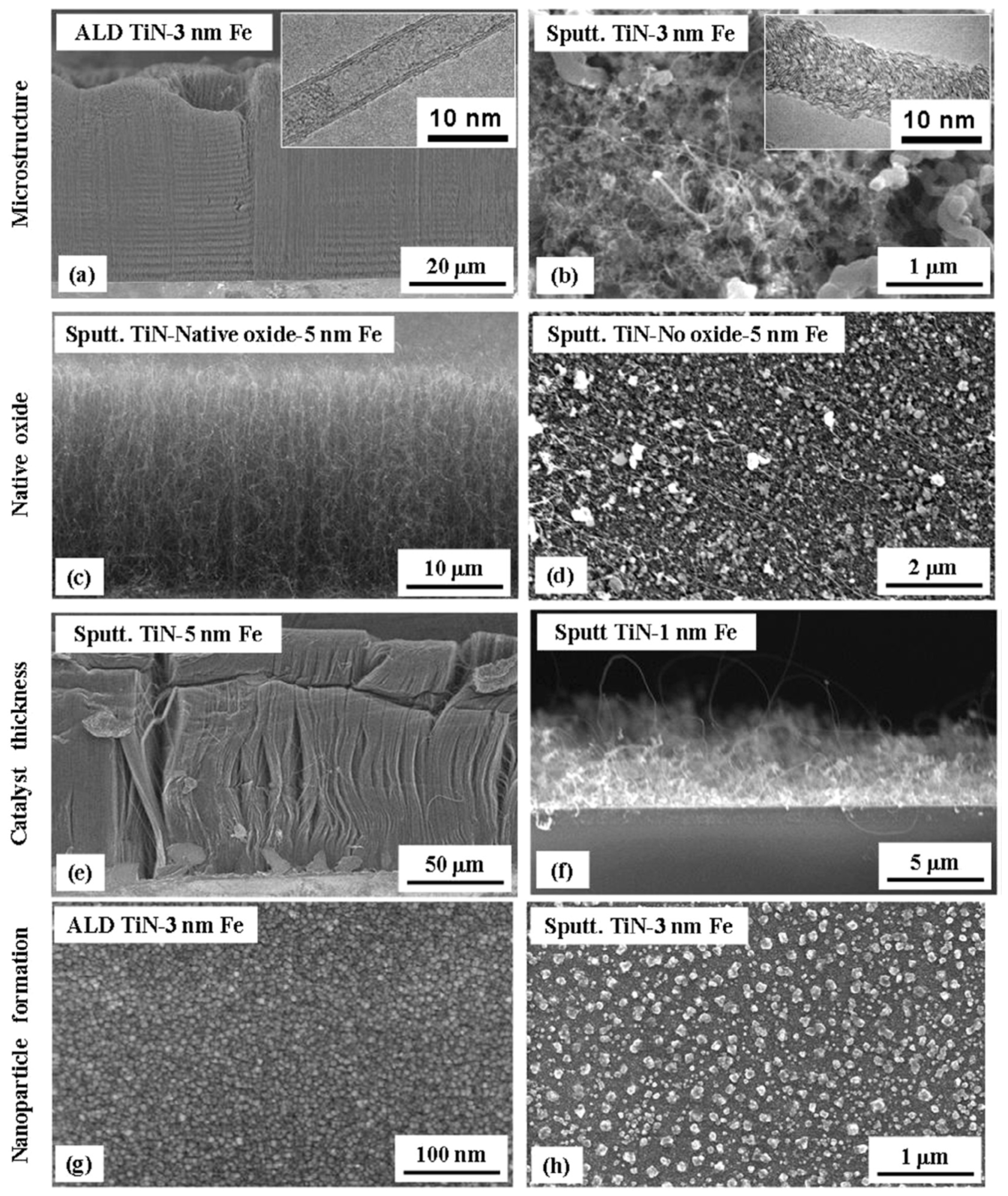
2.3. Via Atomic Layer Deposition (ALD)
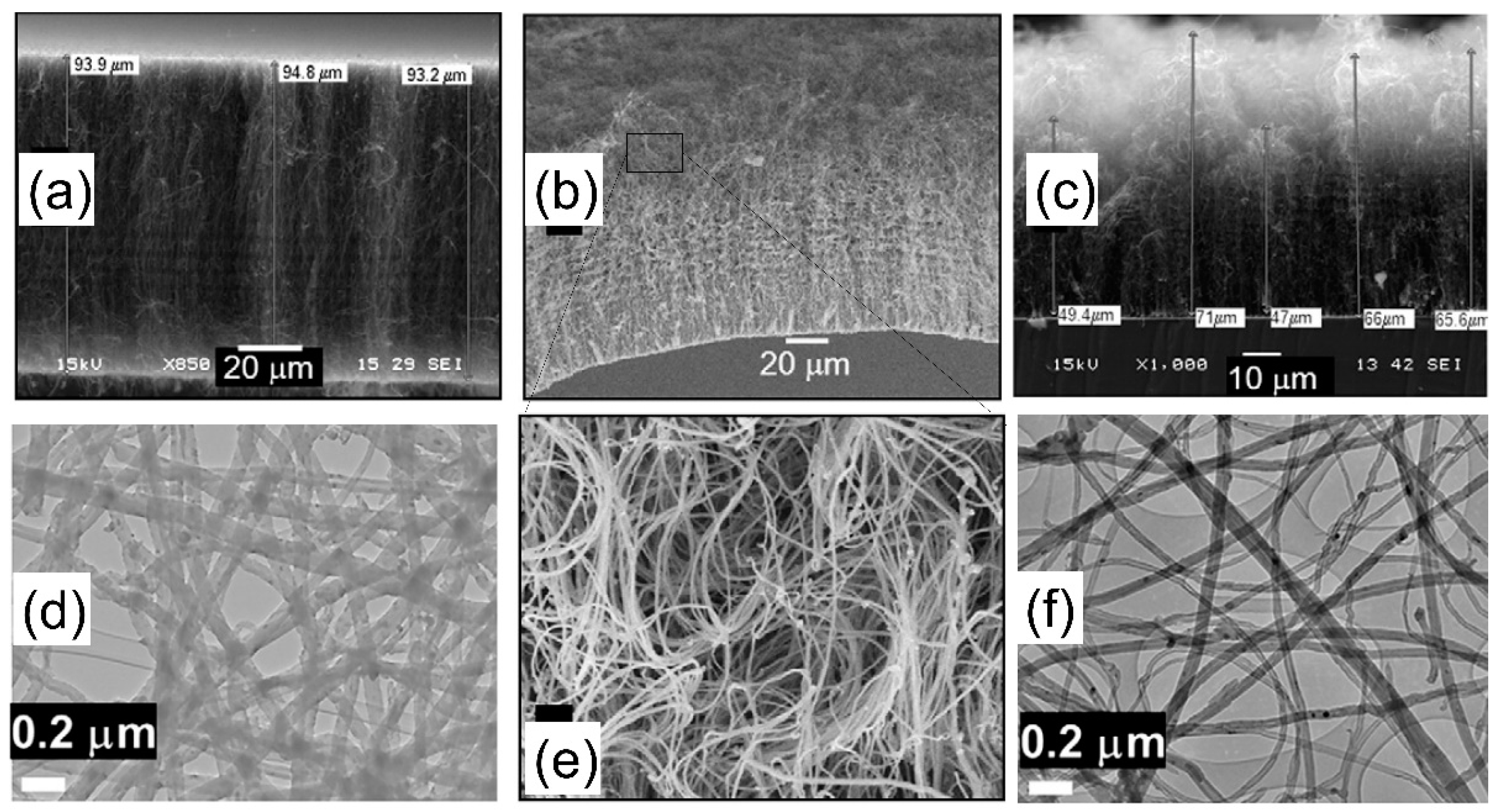
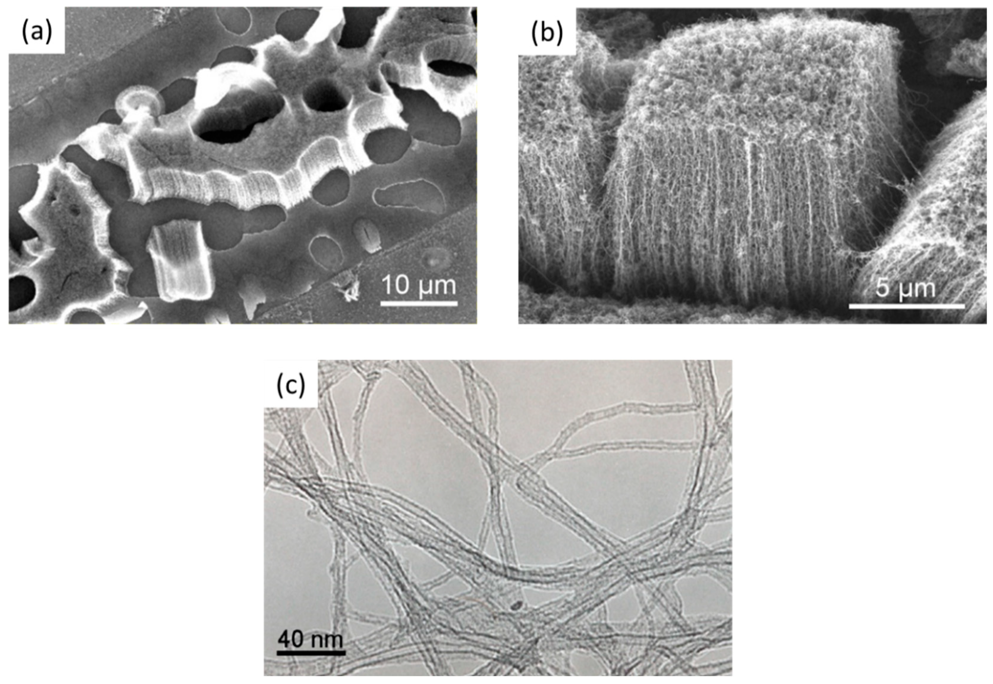
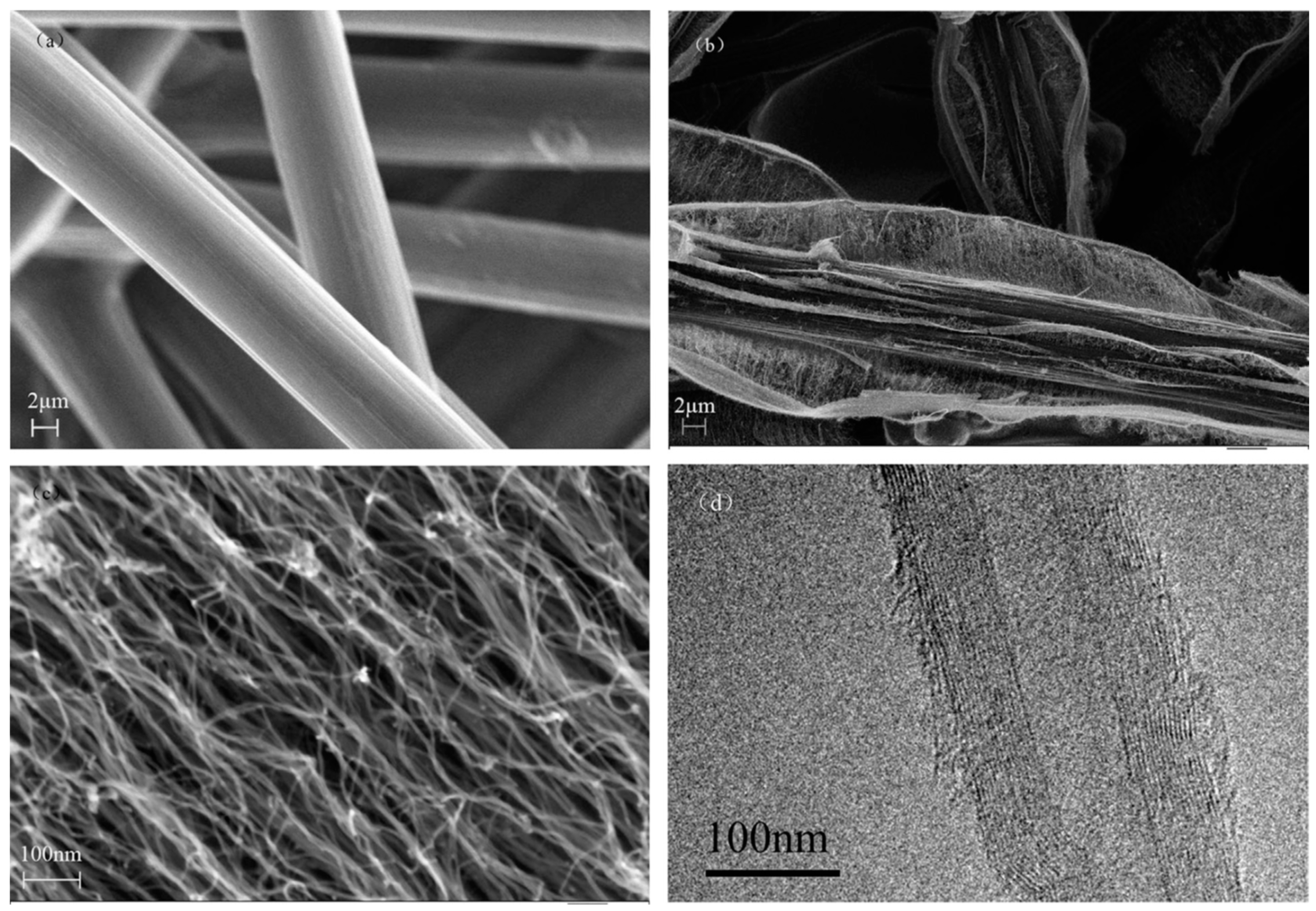
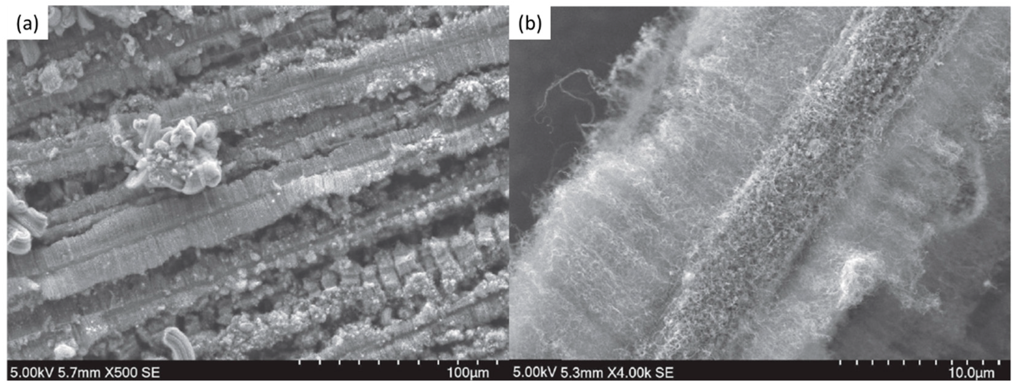
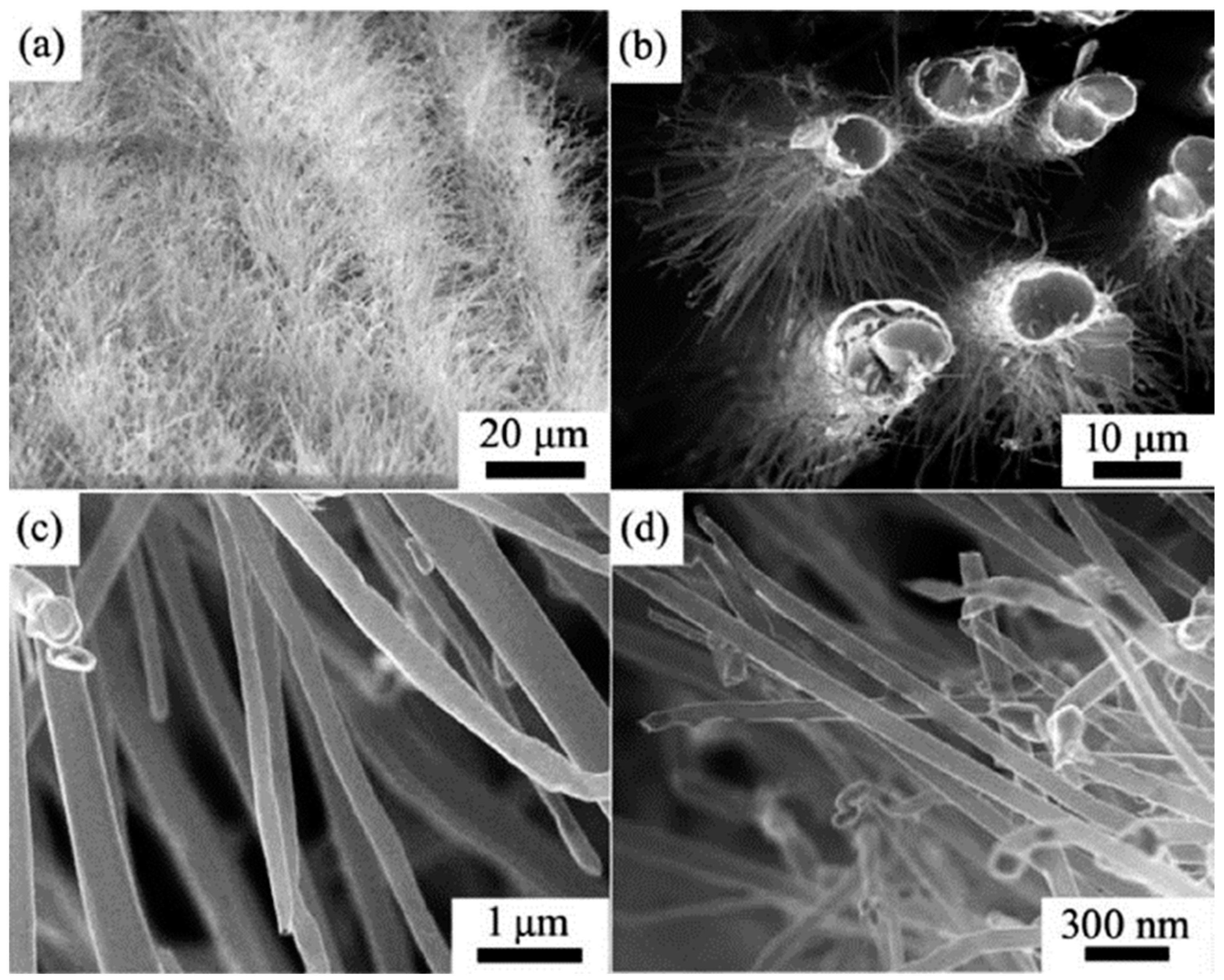
3. Growth of VACNT on Carbon Substrates, with a Focus on CF Substrates
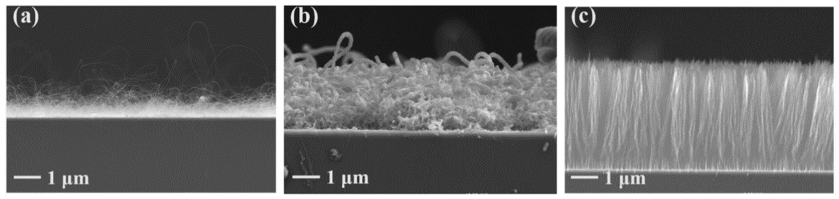
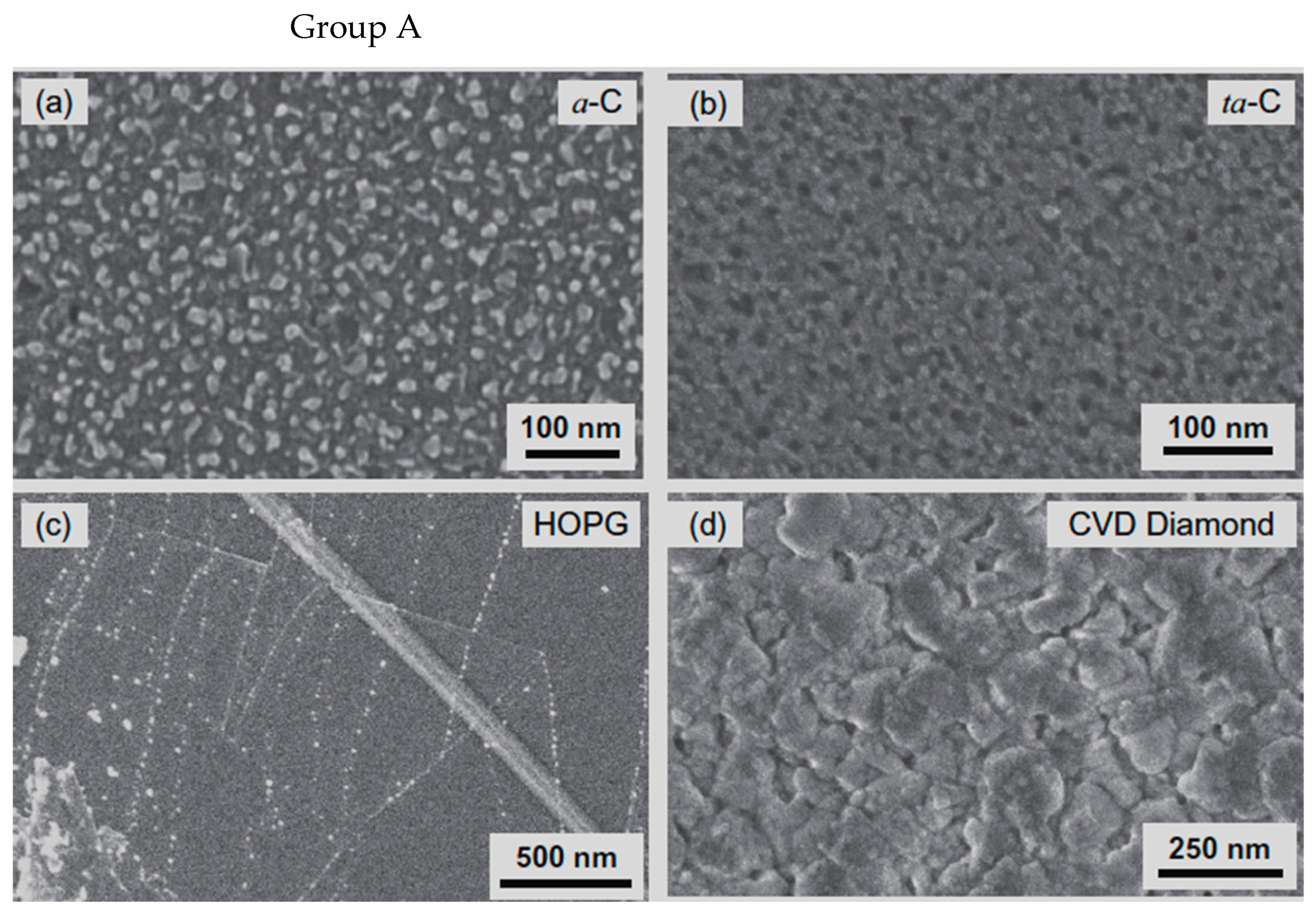
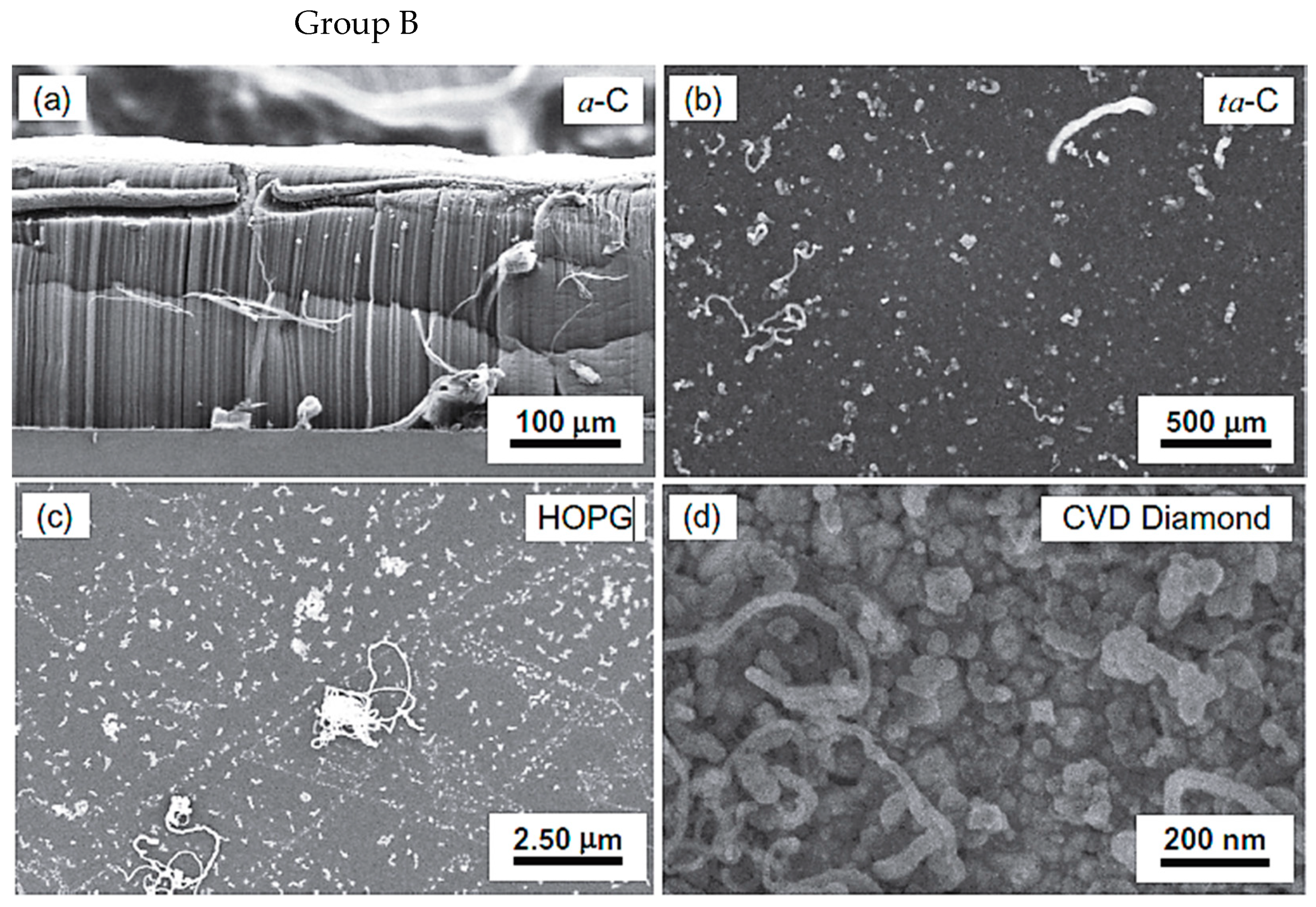
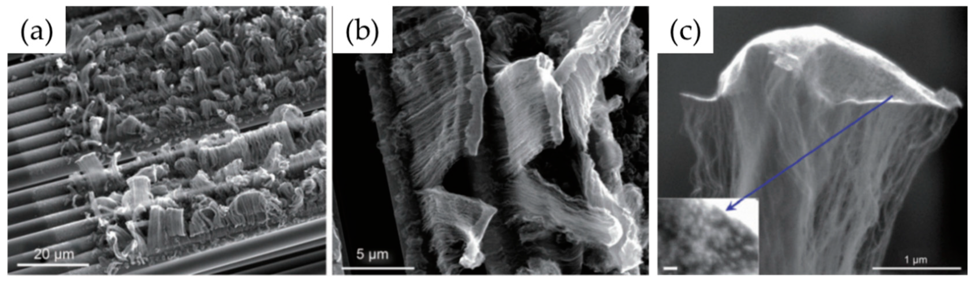
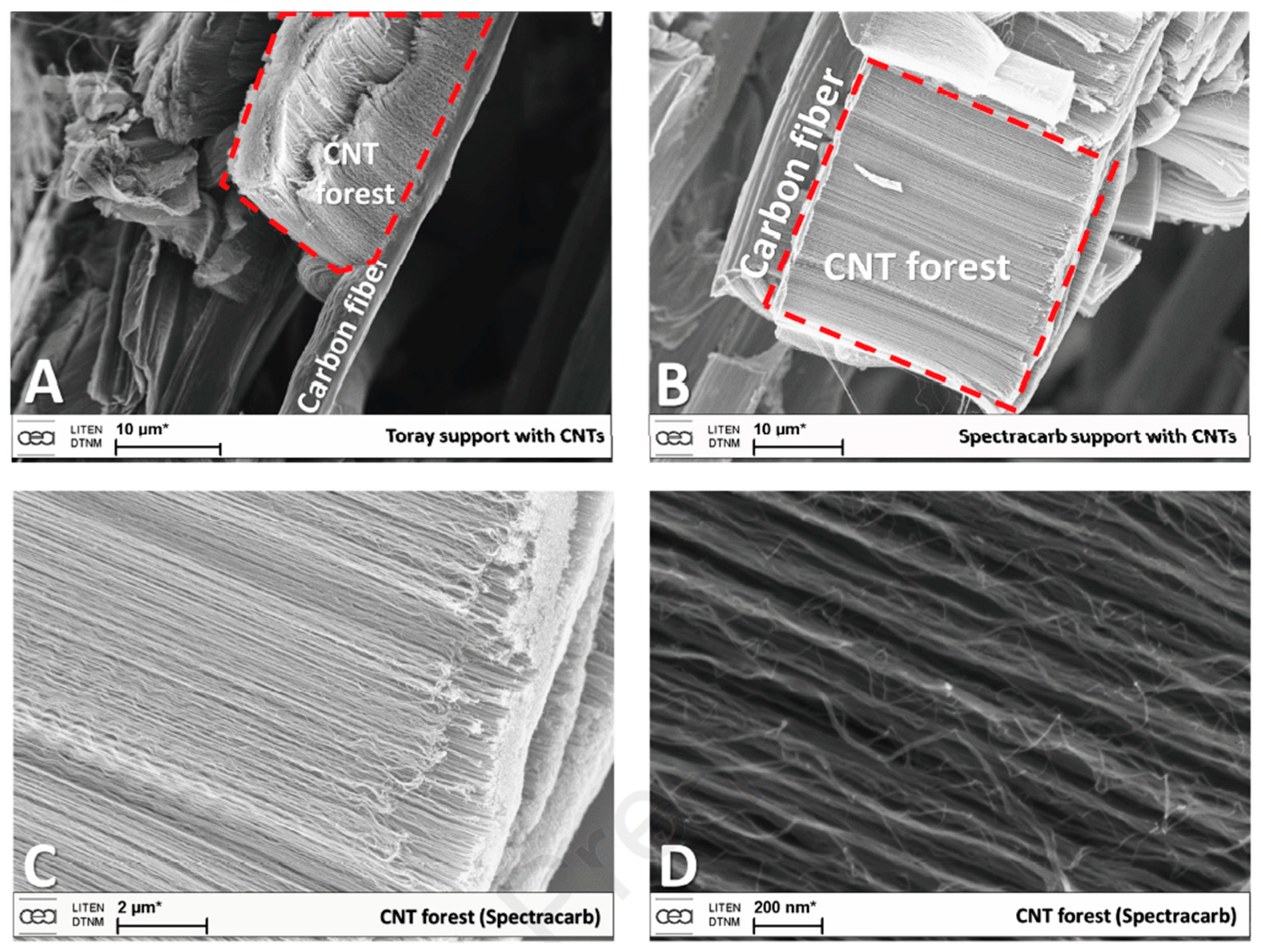
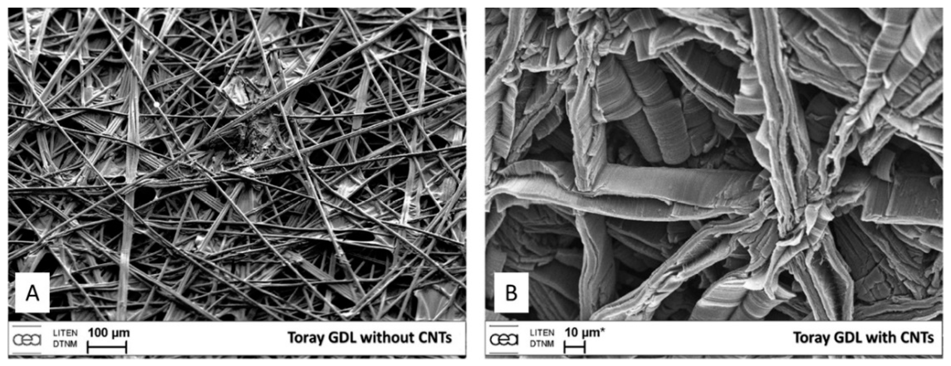
3.1. Growth of VACNT on Carbon Substrates with-/-Out Surface Modifications
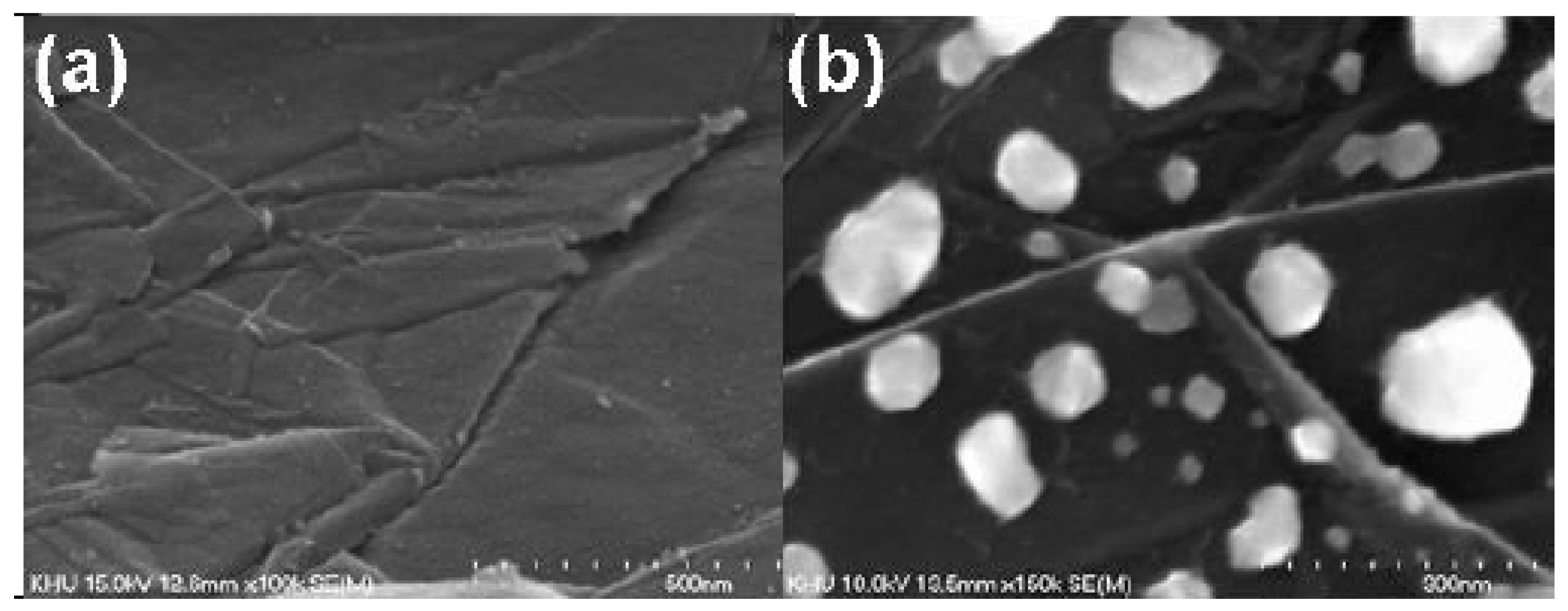
- The properties of some of the examined carbonaceous materials (ex., highly graphitized materials with a precise ratio of 85:15 sp2:sp3 hybridization [32], oxidative plasma-treated HOPG [48], or GP [49]) do not reflect the structural properties of commercially used carbon substrates (as CF, mostly ex-PAN [126,127,128]) available for large-scale industrial use and applications.
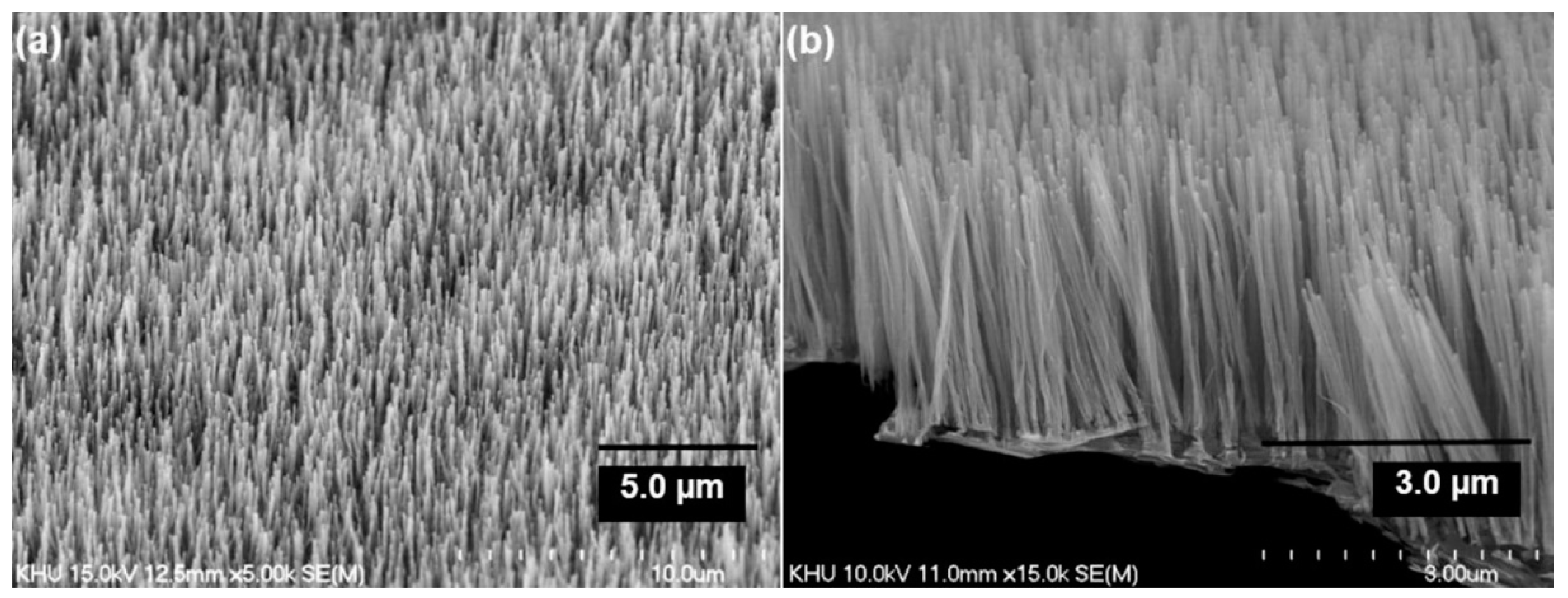
- The composite properties stability, which depends on the controllable growth of VACNT (CNT length/diameter/density), is challenging to achieve when direct growth is performed on CF substrates.
- Presented pre-treatments, such as mild oxidation/activation, of the CF before the growth of VACNT should influence the CF’s structural and physical properties.
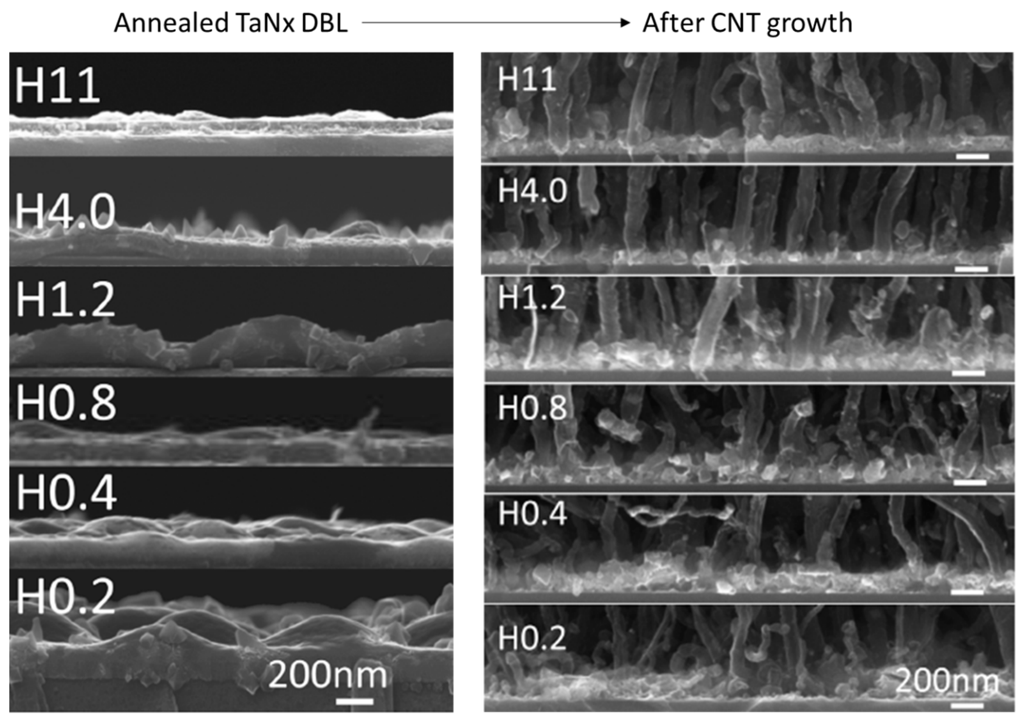
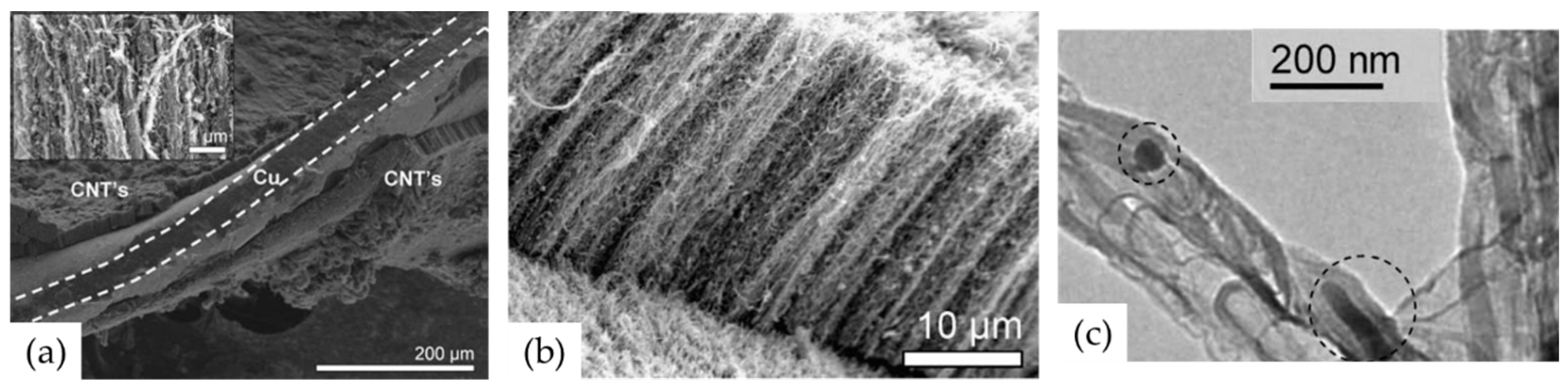
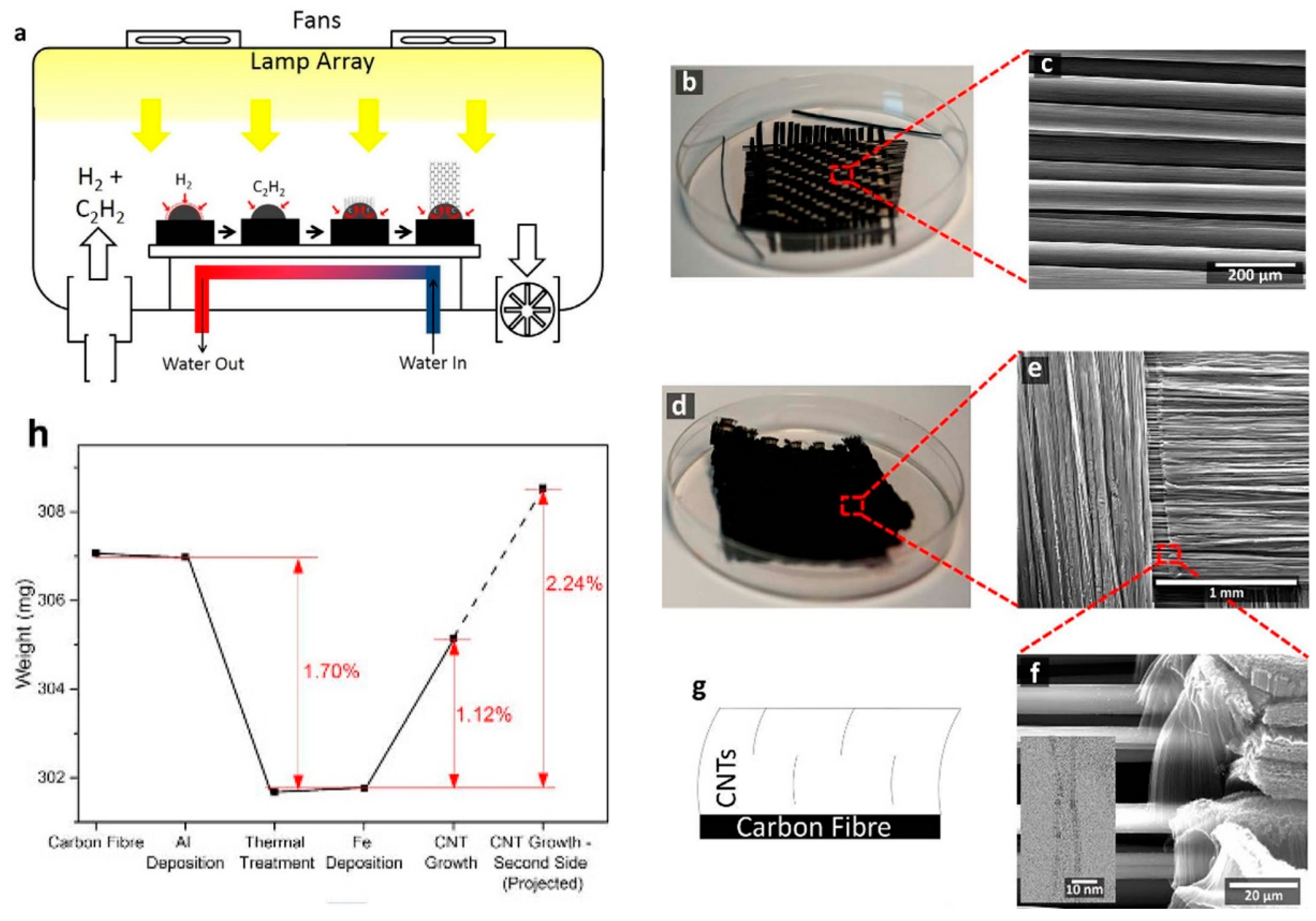
3.2. Deposition of Conducting DBL for Growth of VACNT on Carbon Substrates, with a Focus on CF Substrates
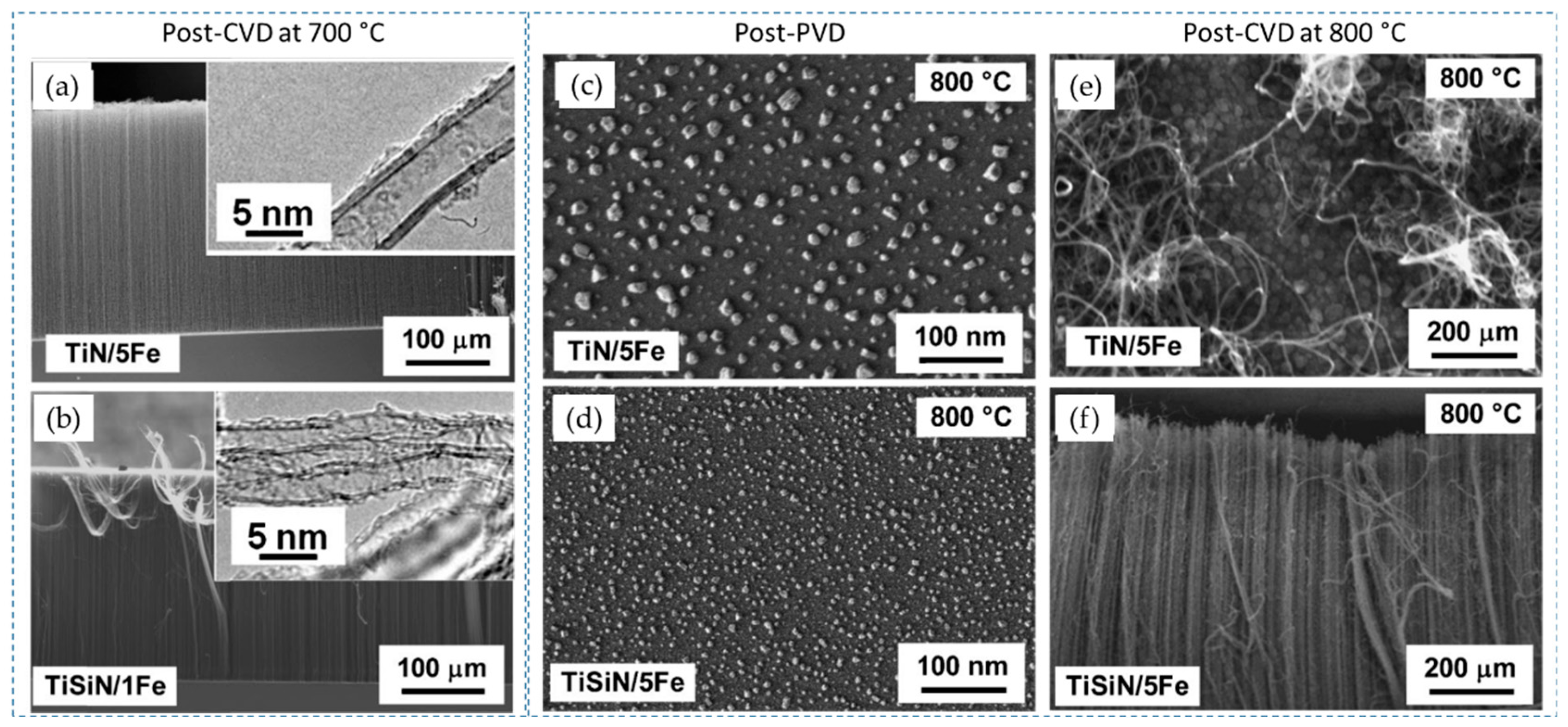
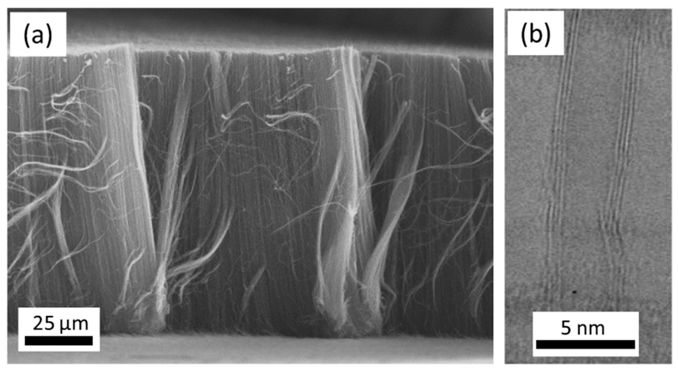
3.2.1. Via Chemical Vapor Deposition (CVD)
3.2.2. Via Physical Vapor Deposition (PVD)
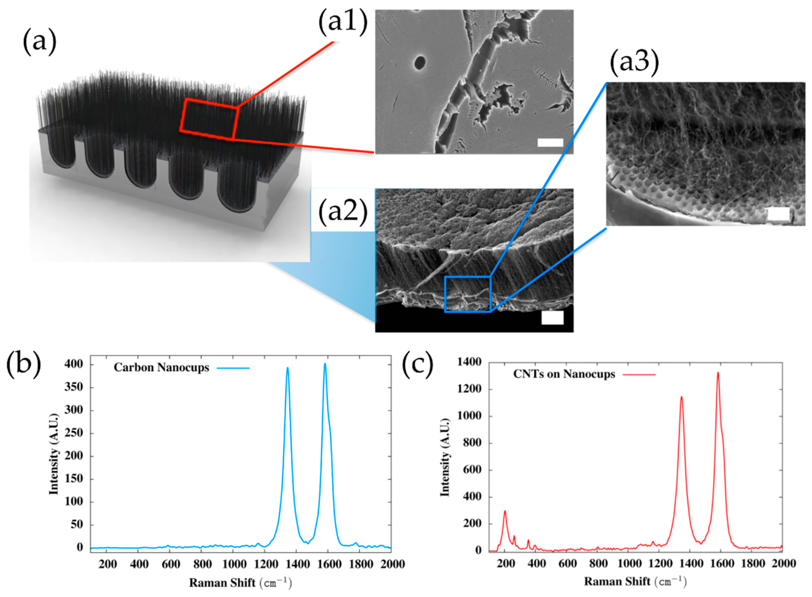
- Use of special engineering approaches to perform precise deposition of a few nanometer layers of alumina with specific physical density and oxidation state;
- To grow VACNT on the catalyst lower layer, a particular joule heating or similar CVD system should be used to stress crack the alumina top layer into small fragments under the sharp increase in temperature at the rate of 300 °C min−1. Thus, deviations in the capping layer thickness and the CVD heating rate can disturb the activation of the Fe catalyst and the VACNT growth;
- The performance of the ‘Odako’ method demands an additional plasma etching process to remove the catalyst-alumina layer standing on the top of the VACNT.
4. Conclusions
Author Contributions
Funding
Data Availability Statement
Conflicts of Interest
References
- Chen, H.; Roy, A.; Baek, J.-B.; Zhu, L.; Qu, J.; Dai, L. Controlled Growth and Modification of Vertically-Aligned Carbon Nanotubes for Multifunctional Applications. Mater. Sci. Eng. R Rep. 2010, 70, 63–91. [Google Scholar] [CrossRef]
- Esteves, L.M.; Oliveira, H.A.; Passos, F.B. Carbon Nanotubes as Catalyst Support in Chemical Vapor Deposition Reaction: A Review. J. Ind. Eng. Chem. 2018, 65, 1–12. [Google Scholar] [CrossRef]
- Soni, S.K.; Thomas, B.; Kar, V.R. A Comprehensive Review on CNTs and CNT-Reinforced Composites: Syntheses, Char-acteristics and Applications. Mater. Today Commun. 2020, 25, 101546. [Google Scholar] [CrossRef]
- Pozegic, T.R.; Anguita, J.V.; Hamerton, I.; Jayawardena, K.D.G.I.; Chen, J.-S.; Stolojan, V.; Ballocchi, P.; Walsh, R.; Silva, S.R.P. Multi-Functional Carbon Fibre Composites Using Carbon Nanotubes as an Alternative to Polymer Sizing. Sci. Rep. 2016, 6, 37334. [Google Scholar] [CrossRef] [PubMed] [Green Version]
- Yoneda, D.; Suzuki, S.; Hiramoto, S.; Matsuoka, Y.; Hara, M.; Yoshimura, M. Growth of Vertically-Aligned Carbon Nano-tubes on Graphite for Electric Double-Layer Capacitors. Mater. Res. Express 2019, 6, 086322. [Google Scholar] [CrossRef]
- Hernández-Vargas, J.; Martinez-Gomez, J.; González-Campos, J.B.; Lara-Romero, J.; Ponce-Ortega, J.M. An Optimization Approach for Producing Carbon Nanotubes Involving Economic and Safety Objectives. Clean Technol. Environ. Policy 2015, 17, 2185–2195. [Google Scholar] [CrossRef]
- Shi, W.; Plata, D.L. Vertically Aligned Carbon Nanotubes: Production and Applications for Environmental Sustainability. Green Chem. 2018, 20, 5245–5260. [Google Scholar] [CrossRef] [Green Version]
- Rao, R.; Pint, C.L.; Islam, A.E.; Weatherup, R.S.; Hofmann, S.; Meshot, E.R.; Wu, F.; Zhou, C.; Dee, N.; Amama, P.B.; et al. Carbon Nanotubes and Related Nanomaterials: Critical Advances and Challenges for Synthesis toward Mainstream Commercial Applications. ACS Nano 2018, 12, 11756–11784. [Google Scholar] [CrossRef] [Green Version]
- Sharma, P.; Pavelyev, V.; Kumar, S.; Mishra, P.; Islam, S.S.; Tripathi, N. Analysis on the Synthesis of Vertically Aligned Carbon Nanotubes: Growth Mechanism and Techniques. J. Mater. Sci. Mater. Electron. 2020, 31, 4399–4443. [Google Scholar] [CrossRef]
- Rakov, E.G. Materials Made of Carbon Nanotubes. The Carbon Nanotube Forest. Russ. Chem. Rev. 2013, 82, 538. [Google Scholar] [CrossRef]
- Vignal, T.; Banet, P.; Pinault, M.; Lafourcade, R.; Descarpentries, J.; Darchy, L.; Hauf, H.; Reynaud, C.; Mayne-L’Hermite, M.; Aubert, P.-H. Electropolymerized Poly(3-Methylthiophene) onto High Density Vertically Aligned Carbon Nanotubes Directly Grown on Aluminum Substrate: Application to Electrochemical Capacitors. Electrochimica Acta 2020, 350, 136377. [Google Scholar] [CrossRef]
- Azam, M.A.; Manaf, N.S.A.; Talib, E.; Bistamam, M.S.A. Aligned Carbon Nanotube from Catalytic Chemical Vapor Dep-osition Technique for Energy Storage Device: A Review. Ionics 2013, 19, 1455–1476. [Google Scholar] [CrossRef]
- Nassoy, F.; Pinault, M.; Descarpentries, J.; Vignal, T.; Banet, P.; Coulon, P.-E.; Goislard de Monsabert, T.; Hauf, H.; Aubert, P.-H.; Reynaud, C.; et al. Single-Step Synthesis of Vertically Aligned Carbon Nanotube Forest on Aluminium Foils. Nanomaterials 2019, 9, 1590. [Google Scholar] [CrossRef] [Green Version]
- Huang, S.; Du, X.; Ma, M.; Xiong, L. Recent Progress in the Synthesis and Applications of Vertically Aligned Carbon Nanotube Materials. Nanotechnol. Rev. 2021, 10, 1592–1623. [Google Scholar] [CrossRef]
- Di Bartolomeo, A.; Scarfato, A.; Giubileo, F.; Bobba, F.; Biasiucci, M.; Cucolo, A.M.; Santucci, S.; Passacantando, M. A Local Field Emission Study of Partially Aligned Carbon-Nanotubes by Atomic Force Microscope Probe. Carbon 2007, 45, 2957–2971. [Google Scholar] [CrossRef] [Green Version]
- Di Bartolomeo, A.; Giubileo, F.; Grillo, A.; Luongo, G.; Iemmo, L.; Urban, F.; Lozzi, L.; Capista, D.; Nardone, M.; Passa-cantando, M. Bias Tunable Photocurrent in Metal-Insulator-Semiconductor Heterostructures with Photoresponse Enhanced by Carbon Nanotubes. Nanomaterials 2019, 9, 1598. [Google Scholar] [CrossRef] [PubMed] [Green Version]
- Andrews, R.; Jacques, D.; Rao, A.M.; Derbyshire, F.; Qian, D.; Fan, X.; Dickey, E.C.; Chen, J. Continuous Production of Aligned Carbon Nanotubes: A Step Closer to Commercial Realization. Chem. Phys. Lett. 1999, 303, 467–474. [Google Scholar] [CrossRef]
- Mayne, M.; Grobert, N.; Terrones, M.; Kamalakaran, R.; Rühle, M.; Kroto, H.W.; Walton, D.R.M. Pyrolytic Production of Aligned Carbon Nanotubes from Homogeneously Dispersed Benzene-Based Aerosols. Chem. Phys. Lett. 2001, 338, 101–107. [Google Scholar] [CrossRef]
- Singh, C.; Shaffer, M.S.P.; Windle, A.H. Production of Controlled Architectures of Aligned Carbon Nanotubes by an Injection Chemical Vapour Deposition Method. Carbon 2003, 41, 359–368. [Google Scholar] [CrossRef]
- Osorio, A.G.; Takimi, A.S.; Bergmann, C.P. Synthesis of Vertically Aligned Carbon Nanotubes by CVD Technique: A Review. In NanoCarbon 2011: Selected works from the Brazilian Carbon Meeting; Avellaneda, C., Ed.; Carbon Nanostructures; Springer: Berlin/Heidelberg, Germany, 2013; pp. 113–124. ISBN 978-3-642-31960-0. [Google Scholar]
- Ahmad, M.; Silva, S.R.P. Low Temperature Growth of Carbon Nanotubes—A Review. Carbon 2020, 158, 24–44. [Google Scholar] [CrossRef]
- Duongthipthewa, A.; Su, Y.; Zhou, L. Electrical Conductivity and Mechanical Property Improvement by Low-Temperature Carbon Nanotube Growth on Carbon Fiber Fabric with Nanofiller Incorporation. Compos. Part B Eng. 2020, 182, 107581. [Google Scholar] [CrossRef]
- Sugime, H.; Sato, T.; Nakagawa, R.; Hayashi, T.; Inoue, Y.; Noda, S. Ultra-Long Carbon Nanotube Forest via in Situ Sup-plements of Iron and Aluminum Vapor Sources. Carbon 2021, 172, 772–780. [Google Scholar] [CrossRef]
- Meysami, S.S.; Koós, A.A.; Dillon, F.; Dutta, M.; Grobert, N. Aerosol-Assisted Chemical Vapour Deposition Synthesis of Multi-Wall Carbon Nanotubes: III. Towards Upscaling. Carbon 2015, 88, 148–156. [Google Scholar] [CrossRef]
- Du, F. Hierarchically Structured Carbon Nanotubes for Energy Conversion and Storage; University of Dayton: Dayton, OH, USA, 2013. [Google Scholar]
- Yang, N.; Youn, S.K.; Frouzakis, C.E.; Park, H.G. An Effect of Gas-Phase Reactions on the Vertically Aligned CNT Growth by Temperature Gradient Chemical Vapor Deposition. Carbon 2018, 130, 607–613. [Google Scholar] [CrossRef]
- A Propos. Available online: http://www.nawatechnologies.com/societe/ (accessed on 31 May 2022).
- Castro, C.; Pinault, M.; Coste-Leconte, S.; Porterat, D.; Bendiab, N.; Reynaud, C.; Mayne-L’Hermite, M. Dynamics of Catalyst Particle Formation and Multi-Walled Carbon Nanotube Growth in Aerosol-Assisted Catalytic Chemical Vapor Deposition. Carbon 2010, 48, 3807–3816. [Google Scholar] [CrossRef]
- Charon, E.; Pinault, M.; Mayne-L’Hermite, M.; Reynaud, C. One-Step Synthesis of Highly Pure and Well-Crystallized Vertically Aligned Carbon Nanotubes. Carbon 2020, 173, 758–768. [Google Scholar] [CrossRef]
- Pinault, M.; Mayne-L’Hermite, M.; Reynaud, C.; Beyssac, O.; Rouzaud, J.N.; Clinard, C. Carbon Nanotubes Produced by Aerosol Pyrolysis: Growth Mechanisms and Post-Annealing Effects. Diam. Relat. Mater. 2004, 13, 1266–1269. [Google Scholar] [CrossRef]
- Fedorovskaya, E.O.; Bulusheva, L.G.; Kurenya, A.G.; Asanov, I.P.; Rudina, N.A.; Funtov, K.O.; Lyubutin, I.S.; Okotrub, A.V. Supercapacitor Performance of Vertically Aligned Multiwall Carbon Nanotubes Produced by Aerosol-Assisted CCVD Method. Electrochimica Acta 2014, 139, 165–172. [Google Scholar] [CrossRef]
- Cartwright, R.J.; Esconjauregui, S.; Weatherup, R.S.; Hardeman, D.; Guo, Y.; Wright, E.; Oakes, D.; Hofmann, S.; Robertson, J. The Role of the Sp2:Sp3 Substrate Content in Carbon Supported Nanotube Growth. Carbon 2014, 75, 327–334. [Google Scholar] [CrossRef]
- Liu, Q.; Shi, X.; Jiang, Q.; Li, R.; Zhong, S.; Zhang, R. Growth Mechanism and Kinetics of Vertically Aligned Carbon Nanotube Arrays. EcoMat 2021, 3, e12118. [Google Scholar] [CrossRef]
- Jiang, Y.Q.; Zhou, Q.; Lin, L. Planar MEMS Supercapacitor Using Carbon Nanotube Forests. In Proceedings of the 2009 IEEE 22nd International Conference on Micro Electro Mechanical Systems, Sorrento, Italy, 25–29 January 2009; pp. 587–590. [Google Scholar]
- Tsuji, T.; Hata, K.; Futaba, D.N.; Sakurai, S. Unexpected Efficient Synthesis of Millimeter-Scale Single-Wall Carbon Nanotube Forests Using a Sputtered MgO Catalyst Underlayer Enabled by a Simple Treatment Process. J. Am. Chem. Soc. 2016, 138, 16608–16611. [Google Scholar] [CrossRef] [PubMed]
- Boulanger, P.; Belkadi, L.; Descarpentries, J.; Porterat, D.; Hibert, E.; Brouzes, A.; Mille, M.; Patel, S.; Pinault, M.; Reynaud, C.; et al. Towards Large Scale Aligned Carbon Nanotube Composites: An Industrial Safe-by-Design and Sustainable Approach. J. Phys. Conf. Ser. 2013, 429, 012050. [Google Scholar] [CrossRef] [Green Version]
- Reit, R.; Nguyen, J.; Ready, W.J. Growth Time Performance Dependence of Vertically Aligned Carbon Nanotube Super-capacitors Grown on Aluminum Substrates. Electrochimica Acta 2013, 91, 96–100. [Google Scholar] [CrossRef]
- Dogru, I.B.; Durukan, M.B.; Turel, O.; Unalan, H.E. Flexible Supercapacitor Electrodes with Vertically Aligned Carbon Nanotubes Grown on Aluminum Foils. Prog. Nat. Sci. Mater. Int. 2016, 26, 232–236. [Google Scholar] [CrossRef] [Green Version]
- Mirea, T.; Olivares, J.; Clement, M.; DeMiguel-Ramos, M.; de Frutos, J.; Sangrador, J.; Iborra, E. Carbon Nanotube Growth on Piezoelectric AlN Films: Influence of Catalyst Underlayers. RSC Adv. 2015, 5, 80682–80687. [Google Scholar] [CrossRef]
- Avasthi, P.; Kumar, A.; Balakrishnan, V. Aligned CNT Forests on Stainless Steel Mesh for Flexible Supercapacitor Electrode with High Capacitance and Power Density. ACS Appl. Nano Mater. 2019, 2, 1484–1495. [Google Scholar] [CrossRef]
- Li, X.; Zhou, J.; Zhang, J.; Li, M.; Bi, X.; Liu, T.; He, T.; Cheng, J.; Zhang, F.; Li, Y.; et al. Bamboo-Like Nitrogen-Doped Carbon Nanotube Forests as Durable Metal-Free Catalysts for Self-Powered Flexible Li–CO2 Batteries. Adv. Mater. 2019, 31, 1903852. [Google Scholar] [CrossRef]
- Li, X.; Gray, E.R.; Islam, A.E.; Sargent, G.A.; Maruyama, B.; Amama, P.B. Magnesia and Magnesium Aluminate Catalyst Substrates for Carbon Nanotube Carpet Growth. ACS Appl. Nano Mater. 2020, 3, 1830–1840. [Google Scholar] [CrossRef]
- Delmas, M.; Pinault, M.; Patel, S.; Porterat, D.; Reynaud, C.; Mayne-L’Hermite, M. Growth of Long and Aligned Multi-Walled Carbon Nanotubes on Carbon and Metal Substrates. Nanotechnology 2012, 23, 105604. [Google Scholar] [CrossRef]
- Patel, S.; Magga, Y.; Belkady, L.; Hibert, E.; Porterat, D.; Boulanger, P.; Pinault, M.; Mayne-L\textquotesingleHermite, M. Development and Optimization of a Secure Injection CVD Process to Grow Aligned Carbon Nanotubes on Large Substrates. J. Phys. Conf. Ser. 2013, 429, 012053. [Google Scholar] [CrossRef] [Green Version]
- Sun, J.; Li, H.; Han, L.; Song, Q. Growth of Radially Aligned Porous Carbon Nanotube Arrays on Pyrolytic Carbon Coated Carbon Fibers. Vacuum 2019, 164, 170–174. [Google Scholar] [CrossRef]
- Liu, H.; Zhang, Y.; Arato, D.; Li, R.; Mérel, P.; Sun, X. Aligned Multi-Walled Carbon Nanotubes on Different Substrates by Floating Catalyst Chemical Vapor Deposition: Critical Effects of Buffer Layer. Surf. Coat. Technol. 2008, 202, 4114–4120. [Google Scholar] [CrossRef]
- Fontana, M.; Ramos, R.; Morin, A.; Dijon, J. Direct Growth of Carbon Nanotubes Forests on Carbon Fibers to Replace Microporous Layers in Proton Exchange Membrane Fuel Cells. Carbon 2020, 172, 762–771. [Google Scholar] [CrossRef]
- Ryu, J.-H.; Lee, G.-J.; Kim, W.-S.; Lim, H.-E.; Mativenga, M.; Park, K.-C.; Park, H.-K. All-Carbon Electrode Consisting of Carbon Nanotubes on Graphite Foil for Flexible Electrochemical Applications. Materials 2014, 7, 1975–1983. [Google Scholar] [CrossRef] [Green Version]
- He, X.; Feng, L.; Song, H.; Zhang, J.; Wei, P.; Jia, X.; Yang, J.; Li, Y.; Shao, D.; Wang, S.; et al. Vertically Aligned Carbon Nanotube@Graphene Paper/Polydimethylsilane Composites for Electromagnetic Interference Shielding and Flexible Joule Heating. ACS Appl. Nano Mater. 2022, 5, 6365–6375. [Google Scholar] [CrossRef]
- Abdollahi, A.; Abnavi, A.; Ghasemi, S.; Mohajerzadeh, S.; Sanaee, Z. Flexible Free-Standing Vertically Aligned Carbon Nanotube on Activated Reduced Graphene Oxide Paper as a High Performance Lithium Ion Battery Anode and Super-capacitor. Electrochimica Acta 2019, 320, 134598. [Google Scholar] [CrossRef]
- Zhang, Q.; Quinton, B.T.; Tsao, B.-H.; Scofield, J.; Merrett, N.; Lawson, J.; Yost, K.; Elston, L. Growth and Characterization of Uniform Carbon Nanotube Arrays on Active Substrates. MRS Online Proc. Libr. 2015, 1752, 3–14. [Google Scholar] [CrossRef]
- Dong, Z.; Sun, B.; Zhu, H.; Yuan, G.; Li, B.; Guo, J.; Li, X.; Cong, Y.; Zhang, J. A Review of Aligned Carbon Nanotube Arrays and Carbon/Carbon Composites: Fabrication, Thermal Conduction Properties and Applications in Thermal Management. New Carbon Mater. 2021, 36, 873–892. [Google Scholar] [CrossRef]
- Badakhsh, A.; An, K.-H.; Kim, B.-J. Enhanced Surface Energetics of CNT-Grafted Carbon Fibers for Superior Electrical and Mechanical Properties in CFRPs. Polymers 2020, 12, 1432. [Google Scholar] [CrossRef]
- Zakaria, M.R.; Md Akil, H.; Abdul Kudus, M.H.; Ullah, F.; Javed, F.; Nosbi, N. Hybrid Carbon Fiber-Carbon Nanotubes Reinforced Polymer Composites: A Review. Compos. Part B Eng. 2019, 176, 107313. [Google Scholar] [CrossRef]
- Pinault, M.; Delmas, M.; L’Hermite, M.M. Growth of Carbon Nanotubes on Carbon or Metal Substrates 2013. U.S. Patent 8,551,618, 8 October 2013. [Google Scholar]
- Seah, C.-M.; Chai, S.-P.; Mohamed, A.R. Synthesis of Aligned Carbon Nanotubes. Carbon 2011, 49, 4613–4635. [Google Scholar] [CrossRef]
- Li, Q.; Sun, S.; Smith, A.D.; Lundgren, P.; Fu, Y.; Su, P.; Xu, T.; Ye, L.; Sun, L.; Liu, J.; et al. Compact and Low Loss Elec-trochemical Capacitors Using a Graphite/Carbon Nanotube Hybrid Material for Miniaturized Systems. J. Power Sources 2019, 412, 374–383. [Google Scholar] [CrossRef]
- Quinton, B.T.; Leedy, K.D.; Lawson, J.W.; Tsao, B.; Scofield, J.D.; Merrett, J.N.; Zhang, Q.; Yost, K.; Mukhopadhyay, S.M. Influence of Oxide Buffer Layers on the Growth of Carbon Nanotube Arrays on Carbon Substrates. Carbon 2015, 87, 175–185. [Google Scholar] [CrossRef]
- Li, S.; Luo, Y.; Lv, W.; Yu, W.; Wu, S.; Hou, P.; Yang, Q.; Meng, Q.; Liu, C.; Cheng, H.-M. Vertically Aligned Carbon Nanotubes Grown on Graphene Paper as Electrodes in Lithium-Ion Batteries and Dye-Sensitized Solar Cells. Adv. Energy Mater. 2011, 1, 486–490. [Google Scholar] [CrossRef]
- Tas, M.O. Carbon Nanotube-Based Hybrid Structures for Micro-Probing and Human Motion Sensing Applications. Ph.D. Thesis, University of Surrey, Guildford, UK, 2020. [Google Scholar]
- Nguyen, J.J.; Turano, S.; Ready, W.J. The Synthesis of Carbon Nanotubes Grown on Metal Substrates: A Review. Nanosci. Nanotechnol. Lett. 2012, 4, 1123–1131. [Google Scholar] [CrossRef]
- Nessim, G.D.; Seita, M.; O’Brien, K.P.; Hart, A.J.; Bonaparte, R.K.; Mitchell, R.R.; Thompson, C.V. Low Temperature Synthesis of Vertically Aligned Carbon Nanotubes with Electrical Contact to Metallic Substrates Enabled by Thermal Decomposition of the Carbon Feedstock. Nano Lett. 2009, 9, 3398–3405. [Google Scholar] [CrossRef]
- Li, G. Substrate and Catalyst Design for Chemical Vapor Deposition Synthesis of Carbon Nanotubes on Si, Cu and SiC; University of Cincinnati: Cincinnati, OH, USA, 2009. [Google Scholar]
- Ng, H.T.; Chen, B.; Koehne, J.E.; Cassell, A.M.; Li, J.; Han, J.; Meyyappan, M. Growth of Carbon Nanotubes: A Combi-natorial Method to Study the Effects of Catalysts and Underlayers. J. Phys. Chem. B 2003, 107, 8484–8489. [Google Scholar] [CrossRef]
- Burt, D.P.; Whyte, W.M.; Weaver, J.M.R.; Glidle, A.; Edgeworth, J.P.; Macpherson, J.V.; Dobson, P.S. Effects of Metal Underlayer Grain Size on Carbon Nanotube Growth. J. Phys. Chem. C 2009, 113, 15133–15139. [Google Scholar] [CrossRef]
- Choi, B.H.; Yoo, H.; Kim, Y.B.; Lee, J.H. Effects of Al Buffer Layer on Growth of Highly Vertically Aligned Carbon Nanotube Forests for in Situ Yarning. Microelectron. Eng. 2010, 87, 1500–1505. [Google Scholar] [CrossRef]
- Dijon, J.; Okuno, H.; Fayolle, M.; Vo, T.; Pontcharra, J.; Acquaviva, D.; Bouvet, D.; Ionescu, A.M.; Esconjauregui, C.S.; Capraro, B.; et al. Ultra-High Density Carbon Nanotubes on Al-Cu for Advanced Vias. In Proceedings of the 2010 International Electron Devices Meeting, San Francisco, CA, USA, 6–8 December 2010; pp. 33.4.1–33.4.4. [Google Scholar]
- Patole, S.P.; Jeong, J.-H.; Yu, S.M.; Kim, H.-J.; Han, J.-H.; Han, I.-T.; Yoo, J.-B. Effect of Buffer Layer Deposition on Diameter and Alignment of Carbon Nanotubes in Water-Assisted Chemical Vapor Deposition. Appl. Surf. Sci. 2013, 271, 32–38. [Google Scholar] [CrossRef]
- Hu, C.-F.; Cheng, C.-L.; Fang, W. The Growth of 3D VA-CNTs Stacks by Predefining Multilayered Al/Fe Catalyst Films for MEMS Fabrication. In Proceedings of the 2013 IEEE 26th International Conference on Micro Electro Mechanical Systems (MEMS), Taipei, Taiwan, 20–24 January 2013; pp. 82–85. [Google Scholar]
- Shah, P.V.; Jha, P.; Gautam, S.; Kumari, M.; Rawat, J.S.; Chaudhury, P.K. Growth Mechanism and Field Emission Behavior of Carbon Nanotubes Grown over 300nm Thick Aluminium Interlayer. Diam. Relat. Mater. 2013, 39, 58–64. [Google Scholar] [CrossRef]
- Vollebregt, S.; Tichelaar, F.D.; Schellevis, H.; Beenakker, C.I.M.; Ishihara, R. Carbon Nanotube Vertical Interconnects Fabricated at Temperatures as Low as 350 °C. Carbon 2014, 71, 249–256. [Google Scholar] [CrossRef]
- Pitkänen, O.; Lorite, G.S.; Shi, G.; Rautio, A.-R.; Uusimäki, A.; Vajtai, R.; Tóth, G.; Kordás, K. The Effect of Al Buffer Layer on the Catalytic Synthesis of Carbon Nanotube Forests. Top. Catal. 2015, 58, 1112–1118. [Google Scholar] [CrossRef]
- Zhong, G.; Yang, J.; Sugime, H.; Rao, R.; Zhao, J.; Liu, D.; Harutyunyan, A.; Robertson, J. Growth of High Quality, High Density Single-Walled Carbon Nanotube Forests on Copper Foils. Carbon 2016, 98, 624–632. [Google Scholar] [CrossRef] [Green Version]
- Zang, X.; Shen, C.; Kao, E.; Warren, R.; Zhang, R.; Teh, K.S.; Zhong, J.; Wei, M.; Li, B.; Chu, Y.; et al. Titanium Disulfide Coated Carbon Nanotube Hybrid Electrodes Enable High Energy Density Symmetric Pseudocapacitors. Adv. Mater. 2018, 30, 1704754. [Google Scholar] [CrossRef] [Green Version]
- Nessim, G.D.; Acquaviva, D.; Seita, M.; O’Brien, K.P.; Thompson, C.V. The Critical Role of the Underlayer Material and Thickness in Growing Vertically Aligned Carbon Nanotubes and Nanofibers on Metallic Substrates by Chemical Vapor Deposition. Adv. Funct. Mater. 2010, 20, 1306–1312. [Google Scholar] [CrossRef]
- Wang, Y.; Luo, Z.; Li, B.; Ho, P.S.; Yao, Z.; Shi, L.; Bryan, E.N.; Nemanich, R.J. Comparison Study of Catalyst Nanoparticle Formation and Carbon Nanotube Growth: Support Effect. J. Appl. Phys. 2007, 101, 124310. [Google Scholar] [CrossRef]
- Bouchet-Fabre, B.; Fadjié-Djomkam, A.; Fernandez-Pacheco, R.; Delmas, M.; Pinault, M.; Jegou, P.; Reynaud, C.; Mayne-L’Hermite, M.; Stephan, O.; Minéa, T. Effect of Tantalum Nitride Supporting Layer on Growth and Morphology of Carbon Nanotubes by Thermal Chemical Vapor Deposition. Diam. Relat. Mater. 2011, 20, 999–1004. [Google Scholar] [CrossRef]
- Bouchet-Fabre, B.; Pinault, M.; Foy, E.; Hugon, M.C.; Minéa, T.; Mayne-L’Hermite, M. Interface Study between Nanostructured Tantalum Nitride Films and Carbon Nanotubes Grown by Chemical Vapour Deposition. Appl. Surf. Sci. 2014, 315, 510–515. [Google Scholar] [CrossRef]
- Lahiri, I. Carbon Nanotube Based Systems for High Energy Efficient Applications. Ph.D. Thesis, Florida International University, Florida, MI, USA, 2011. [Google Scholar]
- Fang, W.-C.; Chen, F.-R.; Tsai, M.-C.; Chou, H.-Y.; Wu, H.-C.; Hsieh, C.-K. Electrochemical Deposited High-Crystallinity Vertical Platinum Nanosheets onto the Carbon Nanotubes Directly Grown on Carbon Paper for Methanol Oxidation. Surf. Coat. Technol. 2017, 320, 584–589. [Google Scholar] [CrossRef]
- De los Arcos, T.; Gunnar Garnier, M.; Oelhafen, P.; Mathys, D.; Won Seo, J.; Domingo, C.; Vicente García-Ramos, J.; Sánchez-Cortés, S. Strong Influence of Buffer Layer Type on Carbon Nanotube Characteristics. Carbon 2004, 42, 187–190. [Google Scholar] [CrossRef]
- Yokoyama, D.; Iwasaki, T.; Yoshida, T.; Kawarada, H.; Sato, S.; Hyakushima, T.; Nihei, M.; Awano, Y. Low Temperature Grown Carbon Nanotube Interconnects Using Inner Shells by Chemical Mechanical Polishing. Appl. Phys. Lett. 2007, 91, 263101. [Google Scholar] [CrossRef]
- García-Céspedes, J.; Thomasson, S.; Teo, K.B.K.; Kinloch, I.A.; Milne, W.I.; Pascual, E.; Bertran, E. Efficient Diffusion Barrier Layers for the Catalytic Growth of Carbon Nanotubes on Copper Substrates. Carbon 2009, 47, 613–621. [Google Scholar] [CrossRef]
- Kpetsu, J.-B.A.; Jedrzejowski, P.; Côté, C.; Sarkissian, A.; Mérel, P.; Laou, P.; Paradis, S.; Désilets, S.; Liu, H.; Sun, X. Influence of Ni Catalyst Layer and TiN Diffusion Barrier on Carbon Nanotube Growth Rate. Nanoscale Res. Lett. 2010, 5, 539–544. [Google Scholar] [CrossRef] [Green Version]
- Amama, P.B.; Pint, C.L.; Mirri, F.; Pasquali, M.; Hauge, R.H.; Maruyama, B. Catalyst–Support Interactions and Their In-fluence in Water-Assisted Carbon Nanotube Carpet Growth. Carbon 2012, 50, 2396–2406. [Google Scholar] [CrossRef]
- Esconjauregui, S.; Bhardwaj, S.; Yang, J.; Castellarin-Cudia, C.; Xie, R.; D’Arsié, L.; Makaryan, T.; Sugime, H.; Eslava, S.; Cepek, C.; et al. Carbon Nanotube Growth on Conductors: Influence of the Support Structure and Catalyst Thickness. Carbon 2014, 73, 13–24. [Google Scholar] [CrossRef]
- Ahmad, M.; Anguita, J.V.; Stolojan, V.; Corless, T.; Chen, J.-S.; Carey, J.D.; Silva, S.R.P. High Quality Carbon Nanotubes on Conductive Substrates Grown at Low Temperatures. Adv. Funct. Mater. 2015, 25, 4419–4429. [Google Scholar] [CrossRef] [Green Version]
- Campo, T.; Pinilla, S.; Gálvez, S.; Sanz, J.M.; Márquez, F.; Morant, C. Synthesis Procedure of Highly Densely Packed Carbon Nanotube Forests on TiN. Nanomaterials 2019, 9, 571. [Google Scholar] [CrossRef] [Green Version]
- Yang, J.; Esconjauregui, S.; Sugime, H.; Makaryan, T.; Hallam, T.; Duesberg, G.S.; Robertson, J. Comparison of Carbon Nanotube Forest Growth Using AlSi, TiSiN, and TiN as Conductive Catalyst Supports. Phys. Status Solidi B 2014, 251, 2389–2393. [Google Scholar] [CrossRef]
- Yang, J.; Esconjauregui, S.; Robertson, A.W.; Guo, Y.; Hallam, T.; Sugime, H.; Zhong, G.; Duesberg, G.S.; Robertson, J. Growth of High-Density Carbon Nanotube Forests on Conductive TiSiN Supports. Appl. Phys. Lett. 2015, 106, 083108. [Google Scholar] [CrossRef] [Green Version]
- Li, S.; Zhou, C.; Raju, S.; Chan, M. Catalyst Design for High-Density and Low-Temperature CNT Synthesis on Conductive Ti Silicide Substrate. Diam. Relat. Mater. 2017, 75, 39–43. [Google Scholar] [CrossRef]
- Hahm, M.G.; Leela Mohana Reddy, A.; Cole, D.P.; Rivera, M.; Vento, J.A.; Nam, J.; Jung, H.Y.; Kim, Y.L.; Narayanan, N.T.; Hashim, D.P.; et al. Carbon Nanotube–Nanocup Hybrid Structures for High Power Supercapacitor Applications. Nano Lett. 2012, 12, 5616–5621. [Google Scholar] [CrossRef] [PubMed]
- Li, H.-H.; Yuan, G.-J.; Shan, B.; Zhang, X.-X.; Ma, H.-P.; Tian, Y.-Z.; Lu, H.-L.; Liu, J. Atomic Layer Deposition of Buffer Layers for the Growth of Vertically Aligned Carbon Nanotube Arrays. Nanoscale Res. Lett. 2019, 14, 119. [Google Scholar] [CrossRef]
- Yuan, G.; Liu, Z.; Cao, Z.; Xie, J.; Li, H.; Li, L.; Sun, Y.; Tian, Y. Direct Growth of Vertically Well-Aligned Carbon Nanotube Arrays on Atomic Layer Deposition of ZnO Films. Chem. Phys. Lett. 2021, 773, 138602. [Google Scholar] [CrossRef]
- Xiang, L.; Yu, P.; Zhang, M.; Hao, J.; Wang, Y.; Zhu, L.; Dai, L.; Mao, L. Platinized Aligned Carbon Nanotube-Sheathed Carbon Fiber Microelectrodes for In Vivo Amperometric Monitoring of Oxygen. Anal. Chem. 2014, 86, 5017–5023. [Google Scholar] [CrossRef]
- Kim, H.; Oh, E.; Hahn, H.T.; Lee, K.-H. Enhancement of Fracture Toughness of Hierarchical Carbon Fiber Composites via Improved Adhesion between Carbon Nanotubes and Carbon Fibers. Compos. Part Appl. Sci. Manuf. 2015, 71, 72–83. [Google Scholar] [CrossRef]
- Vilatela, J.J.; Rabanal, M.E.; Cervantes-Sodi, F.; García-Ruiz, M.; Jiménez-Rodríguez, J.A.; Reiband, G.; Terrones, M. A Spray Pyrolysis Method to Grow Carbon Nanotubes on Carbon Fibres, Steel and Ceramic Bricks. J. Nanosci. Nanotechnol. 2015, 15, 2858–2864. [Google Scholar] [CrossRef] [Green Version]
- Chen, S.; Feng, Y.; Qin, M.; Ji, T.; Feng, W. Improving Thermal Conductivity in the Through-Thickness Direction of Carbon Fibre/SiC Composites by Growing Vertically Aligned Carbon Nanotubes. Carbon 2017, 116, 84–93. [Google Scholar] [CrossRef]
- Ji, T.; Feng, Y.; Qin, M.; Li, S.; Zhang, F.; Lv, F.; Feng, W. Thermal Conductive and Flexible Silastic Composite Based on a Hierarchical Framework of Aligned Carbon Fibers-Carbon Nanotubes. Carbon 2018, 131, 149–159. [Google Scholar] [CrossRef]
- Wang, W. Hierarchical Hybrid Materials from Flexible Fabric Substrates; Wright State University: Dayton, OH, USA, 2020. [Google Scholar]
- Jourdain, V.; Bichara, C. Current Understanding of the Growth of Carbon Nanotubes in Catalytic Chemical Vapour Deposition. Carbon 2013, 58, 2–39. [Google Scholar] [CrossRef] [Green Version]
- Wang, G.; Lu, X.; Ling, Y.; Zhai, T.; Wang, H.; Tong, Y.; Li, Y. LiCl/PVA Gel Electrolyte Stabilizes Vanadium Oxide Nanowire Electrodes for Pseudocapacitors. ACS Nano 2012, 6, 10296–10302. [Google Scholar] [CrossRef] [PubMed]
- Jampani, P.H.; Velikokhatnyi, O.; Kadakia, K.; Hong, D.H.; Damle, S.S.; Poston, J.A.; Manivannan, A.; Kumta, P.N. High Energy Density Titanium Doped-Vanadium Oxide-Vertically Aligned CNT Composite Electrodes for Supercapacitor Applications. J. Mater. Chem. A 2015, 3, 8413–8432. [Google Scholar] [CrossRef]
- Jung, C.Y.; Zhao, T.S.; Zeng, L.; Tan, P. Vertically Aligned Carbon Nanotube-Ruthenium Dioxide Core-Shell Cathode for Non-Aqueous Lithium-Oxygen Batteries. J. Power Sources 2016, 331, 82–90. [Google Scholar] [CrossRef]
- Pibaleau, B. Elaboration et Caractérisation d’électrodes VACNT/MnO2 Pour Application Aux Supercondensateurs Hybrides. Ph.D. Thesis, Université de Tours, Tours, France, 2018. [Google Scholar]
- Jones, A.C.; Hitchman, M.L. Chemical Vapour Deposition: Precursors, Processes and Applications; Royal Society of Chemistry: London, UK, 2009; ISBN 978-0-85404-465-8. [Google Scholar]
- Mandracci, P. Chemical Vapor Deposition for Nanotechnology; BoD—Books on Demand; IntechOpen: London, UK, 2019; ISBN 978-1-78984-960-8. [Google Scholar]
- Cwik, S. Metal Nitride and Metal Disulfide Thin Films via CVD. Ph.D. Thesis, Ruhr University, Bochum, Germany, 2018. [Google Scholar]
- Kafizas, A.; Carmalt, C.J.; Parkin, I.P. CVD and Precursor Chemistry of Transition Metal Nitrides. Coord. Chem. Rev. 2013, 257, 2073–2119. [Google Scholar] [CrossRef]
- Kazadojev, I.I. Growth of V2O5 Films for Electrochromic and Battery Applications. Doctoral Thesis, University College Cork, Cork, Ireland, 2018. [Google Scholar]
- Fix, R.; Gordon, R.G.; Hoffman, D.M. Chemical Vapor Deposition of Titanium, Zirconium, and Hafnium Nitride Thin Films. Chem. Mater. 1991, 3, 1138–1148. [Google Scholar] [CrossRef]
- Mierczynski, P.; Dubkov, S.V.; Bulyarskii, S.V.; Pavlov, A.A.; Skorik, S.N.; Trifonov, A.Y.; Mierczynska, A.; Kitsyuk, E.P.; Gavrilov, S.A.; Maniecki, T.P.; et al. Growth of Carbon Nanotube Arrays on Various CtxMey Alloy Films by Chemical Vapour Deposition Method. J. Mater. Sci. Technol. 2018, 34, 472–480. [Google Scholar] [CrossRef]
- Gromov, D.G.; Bulyarskii, S.; Pavlov, A.; Scorik, S.; Shulyat’ev, A.; Trifonov, A.Y. Catalytic CVD-Growth of Array of Multiwall Carbon Nanotubes on Initially Amorphous Film Co–Zr–N–O. Diam. Relat. Mater. 2016, 64, 97–102. [Google Scholar] [CrossRef]
- Morant, C.; Campo, T.; Márquez, F.; Domingo, C.; Sanz, J.M.; Elizalde, E. Mo–Co Catalyst Nanoparticles: Comparative Study between TiN and Si Surfaces for Single-Walled Carbon Nanotube Growth. Thin Solid Film. 2012, 520, 5232–5238. [Google Scholar] [CrossRef]
- Zhong, G.; Warner, J.H.; Fouquet, M.; Robertson, A.W.; Chen, B.; Robertson, J. Growth of Ultrahigh Density Single-Walled Carbon Nanotube Forests by Improved Catalyst Design. ACS Nano 2012, 6, 2893–2903. [Google Scholar] [CrossRef]
- Baek, J.-K.; Lim, W.; Kim, J.; Ryu, H.J. High Temperature Oxidation Behavior of the Aluminide Coated Refractory Samples in Steam Environment. In Proceedings of the 2017 Spring Meeting of the KNS, Jeju, Korea, 17–19 May 2017. [Google Scholar]
- Yuan, G.-J.; Xie, J.-F.; Li, H.-H.; Lu, H.-L.; Tian, Y.-Z. Atomic Layer Deposition of Inorganic Films for the Synthesis of Vertically Aligned Carbon Nanotube Arrays and Their Hybrids. Coatings 2019, 9, 806. [Google Scholar] [CrossRef] [Green Version]
- Wu, J.; Walenza-Slabe, J.; Mann, M.; Teo, K.B.K.; Milne, W.I.; Jiao, J. Novel Fabrication of Carbon Nanotube Vias for VLSI Interconnects. Microsc. Microanal. 2008, 14, 298–299. [Google Scholar] [CrossRef]
- Gao, J.; Meng, C.; Xie, D.; Liu, C.; Bao, H.; Yang, B.; Li, M.; Yue, Y. Temperature Dependent Thermal Transport in Graphene Paper above Room Temperature. Appl. Therm. Eng. 2019, 150, 1252–1259. [Google Scholar] [CrossRef]
- Rahmanian, S.; Suraya, A.R.; Zahari, R.; Zainudin, E.S. Synthesis of Vertically Aligned Carbon Nanotubes on Carbon Fiber. Appl. Surf. Sci. 2013, 271, 424–428. [Google Scholar] [CrossRef]
- Cherusseri, J.; Kar, K. Self-Standing Carbon Nanotube Forest Electrodes for Flexible Supercapacitors. RSC Adv. 2015, 5, 34335–34341. [Google Scholar] [CrossRef]
- Li, R.; Lachman, N.; Florin, P.; Wagner, H.D.; Wardle, B.L. Hierarchical Carbon Nanotube Carbon Fiber Unidirectional Composites with Preserved Tensile and Interfacial Properties. Compos. Sci. Technol. 2015, 117, 139–145. [Google Scholar] [CrossRef] [Green Version]
- Zhang, J.; Yi, X.; Liu, S.; Fan, H.-L.; Ju, W.; Wang, Q.-C.; Ma, J. Vertically Aligned Carbon Nanotubes/Carbon Fiber Paper Composite to Support Pt Nanoparticles for Direct Methanol Fuel Cell Application. J. Phys. Chem. Solids 2017, 102, 99–104. [Google Scholar] [CrossRef]
- Li, R.; Cornwell, H.; Antunes, E.; Liotta, A.; Parschau, C.; Wardle, B.L. Interlaminar Shear Reinforcement of Aerospace Laminates with Radially-Aligned Carbon Nanotubes. In Proceedings of the 2018 AIAA/ASCE/AHS/ASC Structures, Structural Dynamics, and Materials Conference, Kissimmee, FL, USA, 8–12 January 2018; AIAA SciTech Forum; American Institute of Aeronautics and Astronautics: Reston, VA, USA, 2018. [Google Scholar]
- Russello, M.; Diamanti, E.K.; Catalanotti, G.; Ohlsson, F.; Hawkins, S.C.; Falzon, B.G. Enhancing the Electrical Conductivity of Carbon Fibre Thin-Ply Laminates with Directly Grown Aligned Carbon Nanotubes. Compos. Struct. 2018, 206, 272–278. [Google Scholar] [CrossRef] [Green Version]
- Saha, B.; Schatz, G.C. Carbonization in Polyacrylonitrile (PAN) Based Carbon Fibers Studied by ReaxFF Molecular Dynamics Simulations. J. Phys. Chem. B 2012, 116, 4684–4692. [Google Scholar] [CrossRef]
- Karakashov, B.; Fierro, V.; Mathieu, S.; Gadonneix, P.; Medjahdi, G.; Celzard, A. Structural Characterisation and Chemical Stability of Commercial Fibrous Carbons in Molten Lithium Salts. Materials 2019, 12, 4232. [Google Scholar] [CrossRef] [Green Version]
- Ren, G.; Chen, C.; Deng, L.; Quan, H.; Lu, Y.; Wu, Q. Microstructural Heterogeneity on the Cylindrical Surface of Carbon Fibers Analyzed by Raman Spectroscopy. New Carbon Mater. 2015, 30, 476–480. [Google Scholar] [CrossRef]
- Li, K.-Z.; Song, Q.; Qiang, Q.; Ren, C. Improving the Oxidation Resistance of Carbon/Carbon Composites at Low Tem-perature by Controlling the Grafting Morphology of Carbon Nanotubes on Carbon Fibres. Corros. Sci. 2012, 60, 314–317. [Google Scholar] [CrossRef]
- Song, Q.; Li, K.; Li, H.; Li, H.; Ren, C. Grafting Straight Carbon Nanotubes Radially onto Carbon Fibers and Their Effect on the Mechanical Properties of Carbon/Carbon Composites. Carbon 2012, 50, 3949–3952. [Google Scholar] [CrossRef]
- Pint, C.L.; Alvarez, N.T.; Hauge, R.H. Odako Growth of Dense Arrays of Single-Walled Carbon Nanotubes Attached to Carbon Surfaces. Nano Res. 2009, 7, 526–534. [Google Scholar] [CrossRef] [Green Version]
- Lin, J.; Zhang, C.; Yan, Z.; Zhu, Y.; Peng, Z.; Hauge, R.H.; Natelson, D.; Tour, J.M. 3-Dimensional Graphene Carbon Nanotube Carpet-Based Microsupercapacitors with High Electrochemical Performance. Nano Lett. 2013, 13, 72–78. [Google Scholar] [CrossRef] [PubMed]
- Qiu, L.; Wu, Q.; Yang, Z.; Sun, X.; Zhang, Y.; Peng, H. Freestanding Aligned Carbon Nanotube Array Grown on a Large-Area Single-Layered Graphene Sheet for Efficient Dye-Sensitized Solar Cell. Small 2015, 11, 1150–1155. [Google Scholar] [CrossRef] [PubMed]
- Salvatierra, R.V.; Zakhidov, D.; Sha, J.; Kim, N.D.; Lee, S.-K.; Raji, A.-R.O.; Zhao, N.; Tour, J.M. Graphene Carbon Nanotube Carpets Grown Using Binary Catalysts for High-Performance Lithium-Ion Capacitors. ACS Nano 2017, 11, 2724–2733. [Google Scholar] [CrossRef]
- Sun, S.; Samani, M.K.; Fu, Y.; Xu, T.; Ye, L.; Satwara, M.; Jeppson, K.; Nilsson, T.; Sun, L.; Liu, J. Improving Thermal Transport at Carbon Hybrid Interfaces by Covalent Bonds. Adv. Mater. Interfaces 2018, 5, 1800318. [Google Scholar] [CrossRef]
- Hansson, J.; Li, Q.; Smith, A.; Zakaria, I.; Nilsson, T.; Nylander, A.; Ye, L.; Lundgren, P.; Liu, J.; Enoksson, P. Bipolar Electrochemical Capacitors Using Double-Sided Carbon Nanotubes on Graphite Electrodes. J. Power Sources 2020, 451, 227765. [Google Scholar] [CrossRef]
- Chen, L.-H.; AuBuchon, J.F.; Chen, I.-C.; Daraio, C.; Ye, X.-R.; Gapin, A.; Jin, S.; Wang, C.M. Growth of Aligned Carbon Nanotubes on Carbon Microfibers by Dc Plasma-Enhanced Chemical Vapor Deposition. Appl. Phys. Lett. 2006, 88, 033103. [Google Scholar] [CrossRef] [Green Version]
- Pozegic, T.R.; Hamerton, I.; Anguita, J.V.; Tang, W.; Ballocchi, P.; Jenkins, P.; Silva, S.R.P. Low Temperature Growth of Carbon Nanotubes on Carbon Fibre to Create a Highly Networked Fuzzy Fibre Reinforced Composite with Superior Electrical Conductivity. Carbon 2014, 74, 319–328. [Google Scholar] [CrossRef]


| Substrate | DBL via PVD/PVD Conditions for DBL/Catalyst | Process of CVD/Carbon Source | Carrier or Carbon Source Gas: Flow Rate/Mixture (m3 s−1, Unless Otherwise Specified) | Pressure (Pa)/Temperature (K)/Reaction Duration (min) | CNT Average Diameter (nm) | CNT Length (µm) | Density of VACNT (Tubes cm−2) | DBL/VACNT/Composite Properties | Reference |
|---|---|---|---|---|---|---|---|---|---|
| Si coated with native SiO2 or additional 300 nm thick SiO2 top-layer | 10 nm Al DBL via magnetron sputtering/Chamber pressure (5 × 10⁻⁸ Pa); Operating gas pressure (7 × 10⁻¹ Pa); Operating gas Ar at 2 Pa; Operating temperature: 293.15, 320.15, 373.15, 473.15 K/0.5 nm Ni catalyst deposited via electron beam evaporation at a rate of 0.01 nm s−1 (post-transfer in air) | Alcohol assisted thermalCVD (tube furnace)/C2H5OH and H2 | - CNT Synthesis: H2:C2H5OH:Ar = 1.3 × 10⁻⁷: 1.2 × 10⁻⁵: 2 × 10⁻⁵ | Patm/1073/Annealing (5); Synthesis (20) | 7 | 30–40 | - | - Use of metal alloy as DBL/catalyst layer - Growth of single-wall VACNT | [65] |
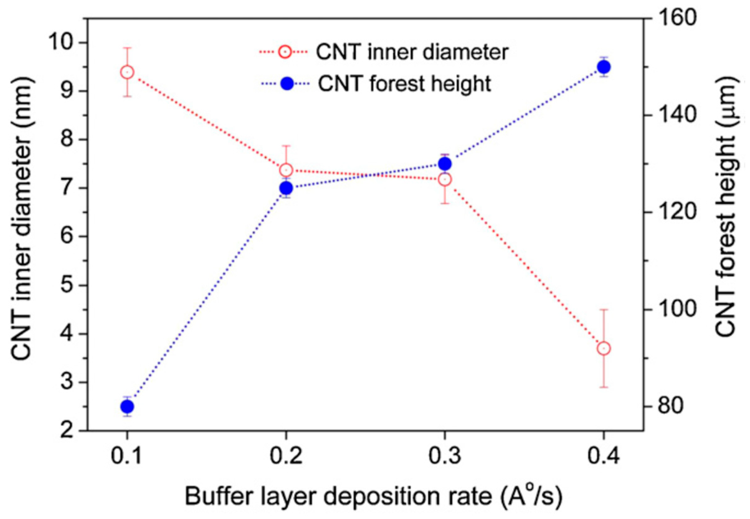
| Si coated with 4 nm native SiO2 | 18 nm Al DBL via electron beam evaporation/Chamber pressure (0.0007 Pa); Operating temperature: 293.15 K; Deposition rate: 0.1, 0.2, 0.3 and 0.4 Å s−1/2 nm Fe catalyst deposited via electron beam evaporation at 0.1 Å s−1 (break of vaccum before the Fe deposition) | Water-assisted CVD/Ar, H2O vapors and C2H2 | - | 3.23/973/Annealing (6); Synthesis (10) | - CNT inner diameter: 4–9 nm (0.4–0.1 Å s−1) - Number of walls in CNT: 6–8 (0.4–0.1 Å s−1) | 78–150 (0.1–0.4 Å s−1) | - | - Growth of multi-walled VACNT | [68] |
| Si coated with SiO2 with 300 nm thickness | 30 nm Al DBL via magnetron sputtering/Operating temperature: 293.15 K/0.5 nm Fe catalyst deposited via electron beam evaporation (post transfer in air) | Thermal CVD (quartz tube reactor)/C2H2 and He | - Annealing: He 20 slm; - CNT Synthesis: He 20 slm; C2H2 6.7 × 10⁻⁶; | Patm/1053/Annealing (20); Synthesis (15) | - | 1330 | 3 × 10¹⁰ | - 5 cm long CNT yarns from twisted CNT. | [66] |
| Substrate | DBL via PVD/PVD Conditions for DBL/Catalyst | Process of CVD/Carbon Source | Carrier or Carbon Source Gas: Flow Rate/Mixture (m3 s−1, Unless Otherwise Specified) | Pressure (Pa)/Temperature (K)/Reaction Duration (min) | CNT Average Diameter (nm) | CNT Length (µm) | Density of VACNT (tubes cm−2) | DBL/VACNT/Composite Properties | Reference |
|---|---|---|---|---|---|---|---|---|---|
| Poly Si wafer | Co-Al (99.5%) /-/1 nm of Fe catalyst film | pure-thermal/C2H2, H2, and He | Ratio data: C2H2:H2:He = 1:5:5 | 100/853/- | ~4–5 | 2–30 | Up to 2.5 × 10¹² | - Growth of double-/triple--walled VACNT - Electrical conductivity measured by AFM tip on CNT carpet with a contact force of 100 µN or 1N, measured minimal resistance of ~20 Ω or ~2.1 Ω, respectively. The resistance linearly increased with the CNT length. | [67] |
| 400 µm thick Cu foils (99.99% Cu, Vortex metals, Inc., Warrensville Heights, OH, USA) | 5–10–15–30 nm Al DBL via RF sputtering (DV-502A, Denton Co., Cardiff, UK)/-/Catalyst introduced during CVD: ferrocenne/m-xylene (10 kg m−3) | Floating catalyst CVD (quartz tube reactor)/Carbon source: ferrocene/m-xylene (10 kg m−3) with Ar and H2 as carrier gas | - CNT Synthesis: H2 8.3 × 10⁻⁷; C2H2 1.6 × 10⁻⁶; | Patm/1023/Annealing (20); Synthesis (15) | 10–100 | 30–50 | - | - Interfacial adhesion (pull-off tests) tests: around 0.2 to 0.4 MPa as for 10 to 30 nm Al DBL composites, respectively. | [51] |
| 25 µm thick Cu foils (99.8% Cu, Alfa Aesar, No: 046365.RH) | 6 nm Al DBL via DC magnetron sputtering/Chamber pressure (1 × 10⁻⁶ Pa); Operating gas pressure (3.5 × 10⁻³ Pa); Operating gas Ar; DBL deposition rate: 0.022 nm s−1/Successive deposition of 0.4 nm Fe catalyst; Deposition rate: 0.018 nm s−1 + additional deposition of 0.4 nm Al top layer | Cold-wall CVD/C2H2 and H2 | - Annealing: H2 8.3 × 10⁻⁶; - CNT Synthesis: 98% H2/2% C2H2 = 8.3 × 10⁻⁶; | (1.5 × 10³)/Annealing (953); Synthesis (1033)/Annealing (1.5); Synthesis (0.5) | 1.9 | 9.2 | 2.2 × 10¹² | - Bi-modal SWCNT diameter distribution - Resistivity of SWCNT-Al DBL- Cu composite: 60–80 Ohms | [73] |
| Conducting brass (Cu-Zn alloys), copper, stainless steel, Inconel® 600, silicon, and alumina | 2–5–10–20 nm Al DBL via RF sputtering/-/1 nm Fe catalyst deposited via electron beam evaporation (air introduced between the Al DBL and the Fe PVD steps) | Cold-wall low-pressure CVD/C2H2 and H2 | - Annealing: H2 1 × 10⁻⁵; - CNT Synthesis: H2 ?/C2H2 ? | (5 × 10³)/Annealing (973); Synthesis (933)/Annealing (5); Synthesis (10) | 7 | 46–312 (depen-ending on DBL thickness and susbtrate type) | - | - Growth of multi-walled VACNT; - Total electric resistance ranging below 10 Ω; - Specific capacitances were measured to be 8.1 ± 0.6, 7.9 ± 0.4, and 10.0 ± 0.4 F g−1 for VACNT on Inconel® 600, Cu, and stainless steel, respectively, (Cyclic voltammetry measurements in aqueous KOH electrolytes) | [72] |
| TiSi | 2 nm Ni—1 nm Al—2 nm Ni was deposited by electron beam evaporation/Chamber pressure (4 × 10⁻⁵ Pa); deposition rate: 0.2 Å s−1 | 200 W Plasma-enhanced CVD/CH4 and H2 | - Annealing: H2:N2 = 5 × 10⁻⁸: 1.6 × 10⁻⁸; - CNT Synthesis: H2:N2 = 5 × 10⁻⁸: 1.6 × 10⁻⁸ + 35 sccm CH4 | 370/923/Annealing (10); Synthesis (1) | ~43.6 | 4.5 | 2 × 10¹⁰ | - Growth of thick multi-walled VACNT; - Achieved Ohmic contact between the Ti silicide and the VACNT with a total resistance of 540 Ω. | [91] |
| Substrate | DBL via PVD/PVD Conditions for DBL/Catalyst | Process of CVD/Carbon source | Carrier or Carbon Source Gas: Flow Rate/Mixture (m3 s−1) | Pressure (Pa)/Temperature (K)/Reaction Duration (min) | CNT Average Diameter (nm) | CNT Length (µm) | Density of VACNT (tubes cm−2) | DBL/VACNT/Composite Properties | Reference |
|---|---|---|---|---|---|---|---|---|---|
| Oxidized Si/SiO2 coupons | 30 nm Ta via electron-beam evaporation/Operating gas pressure (3.5 × 10⁻⁴–3.5 × 10⁻⁵ Pa)/Electron-beam evaporation of 5 nm Fe catalyst film | Fast-heat 3 zone thermal/C2H4 | Ar (3.3 × 10⁻⁶): C2H4 (2.5 × 10⁻⁶): H2 (6.6 × 10⁻⁶) | Patm/Furnace zone I and II -annealing step (1023); Zone III—CNT growth (748)/(45) | ~22 | ~2 | - | - Electrical conductivity measured by AFM tip on contact with CNT carpet, measured resistance ~35 kΩ | [62] |
| Si wafer | 130 nm TaN via conventional radio frequency (RF:400 W) magnetron sputtering/Operating gases N2 (3 × 10⁻⁸–3 × 10⁻⁷ m3 s−1) + Ar (1.7 × 10⁻⁶ m3 s−1); Operating gas pressure (5 Pa)/2.5% ferrocene in toluene | aerosol-assisted catalytic/toluene | Ar (5 × 10⁻⁵) | Patm/(1123)/(12) | ~60–150 | ~40–150 | - | - | [77] |
| Si wafer | Post-deposition 60 nm and post-annealing 60–240 nm TaN thickness via highly pulsed power magnetron sputtering/Operating gases (N2+Ar)/5% ferrocene in toluene | aerosol-assisted catalytic/toluene | Ar | Patm/(1123)/(15) | ~40–110 | ~45–195 | - | - | [78] |
| Si coated with SiO2 | 25 nm Co-Zr-N-(O) DBL via DC magnetron sputtering with Zr target/Chamber pressure (10−3 Pa); Operating gas pressure (0.7 Pa); Operating gas Ar/N2 ratio: 10/80 vol. %/Co target (final atomic concentration 30–35%) | Plasma System in CVD mode without plasma/C2H2 and H2 | - CNT Synthesis: NH3:C2H2:Ar = 1.6 × 10⁻⁸: 1.6 × 10⁻⁸: 5 × 10⁻⁸ | -/783/Annealing (/); Synthesis (10) | 7 | 30–40 | - | - Use of metal alloy as DBL/catalyst layer - Growth of multi-walled VACNT | [112] |
| Substrate | DBL via PVD/PVD Conditions for DBL/Catalyst | Process of CVD/Carbon Source | Carrier or Carbon Source Gas: Flow Rate/Mixture (m3 s−1) | Pressure (Pa)/Temperature (K)/Reaction Duration (min) | CNT Average Diameter (nm) | CNT Length (µm) | Density of VACNT (tubes cm−2) | DBL/VACNT/Composite Properties | Reference |
|---|---|---|---|---|---|---|---|---|---|
| Laminated copper sheets | 20 nm TiN via magnetron sputtering/Operating gas N2+Ar; Operating temperature: 293 K/8.76% ferrocene in toluene as catalyst/carbon source (injection rate: 5.6 cm3 h−1 in preheated evaporator at 453 K | Pure-thermal CVD (tube reactor)/- | - Annealing and CNT Synthesis: Ar (4.2 × 10⁻⁵): H2 (4.2 × 10⁻⁶) | ≥Patm/(973)/Annealing (10); Synthesis (20) | 20–30 | - Growth of bamboo-like multi-walled VACNT with intence structural defects; | [83] | ||
| P-type silicon wafers (100) El-CAT Inc., Ridgefield Park, NJ, USA | 200 nm TiN via Dual Ion Beam Sputtering (DIBS) with TiN target (99.5% purity)/Operating gas N2+Ar; Operating temperature: 493 K; Duration 240 min/Mo(CH3COO)2 (0.04% p/v) and Co(CH3COO)2·4H2O (0.02% p/v) in C2H5OH via dip-coating. | alcohol catalytic/N2 flow saturated with ethanol:water (99.5:0.5 v/v) | - Annealing: Ar (4 × 10⁻⁶); - CNT Synthesis: N2 (4 × 10⁻⁶): H2 (1.3 × 10⁻⁶): EtOH (8.3 × 10⁻⁶) | Patm/(1073, 30 K min−1)/Annealing (10); Synthesis (20) | ~3–5 | ~8 | - | - Field emission performance under therein given conditions | [88] |
| Si coated with 200 nm thermal SiO2 | 50 nm TiSiN, or TiN DBL via sputtering/-/1 (for TiSiN), or 5 nm (for TiN) Fe catalyst deposited via evaporation (air introduced between the DBL and the Fe PVD steps) | Hot-wall CVD (quartz tube reactor)/C2H2 and H2 | - Annealing:Ar:H2 = 1.6 × 10⁻⁵ : 8.3 × 10⁻⁶; - CNT Synthesis: C2H2:Ar:H2 = 1.6 × 10⁻⁷:1.6 × 10⁻⁵: 8.3 × 10⁻⁶; | Patm/973, 100 K min−1/Annealing (5); Synthesis (15) | ~5 (TiSiN); ~6–9 (TiN) | ~200–300 | ~1012 (TiSiN); ~1010 (TiN) | - Growth of multi-walled VACNT - Air current–voltage measurements with two-terminal probe station yield resistance values of 0.8 and 3.4 kΩ for TiSiN and TiN, respectively. | [89] |
| Substrate | DBL via PVD/PVD Conditions for DBL/Catalyst | Process of CVD/Carbon Source | Carrier or Carbon Source Gas: Flow Rate/Mixture (m3 s−1) | Pressure (Pa)/Temperature (K)/Reaction Duration (min) | CNT Average Diameter (nm) | CNT Length (µm) | Density of VACNT (tubes cm−2) | DBL/VACNT/Composite Properties | Reference |
|---|---|---|---|---|---|---|---|---|---|
| Si coated with native SiO2 | 50 nm TiSiN using MaTecK GmbH TiSiN target and 6 keV Ar ions/-/0.4 nm Fe catalyst + 0.1 nm Al (top-cover) deposited via magnetron sputtering in 0.35 Pa of Ar at 20 W (air transfer between the PVD and CVD steps) | Pure-thermal CVD (tube reactor)/C2H2 and H2 | - Annealing: Ar:H2 = 1.6 × 10⁻⁵:8.3 × 10⁻⁶; - CNT Synthesis: C2H2:Ar:H2 = 1.6 × 10⁻⁷:1.6 × 10⁻⁵:8.3 × 10⁻⁶; | Patm/873/Annealing (5); Synthesis (15) | ~3 | ~100 | 5.1 × 10¹² | - Growth of double-/triple--walled VACNT - Two-point probe measurements present Ohmic contact with overall nanotubes-TiSiN support resistance of 0.7 ± 0.05 kΩ; | [90] |
| Si wafer | 8 nm Al on 100 nm TiN (Al or TiN targetS WITH 99.95% purity) by PVD DC magnetron sputtering /Chamber pressure (0.7 Pa); Operating gas: Ar 25 + N (for TiN) (4.2 × 10⁻⁷ m3 s−1); PVD duration: 3 min Al+ 50 minTiN/3 nm Fe via DC magnetron sputtering | photo-thermal/C2H2 and H2 | H2 (1.6 × 10⁻⁶); C2H2 (4.2 × 10⁻⁷) | (1.3 × 10³)/(~1023 catalyst surface; ~898-728 at bottom of Si substrate)/Annealing (10); CNT Growth (15) | ~6 ± 3 | 473 ± 44 | 1010 | - As grown VACNT network probe resistance: 10 Ω - Improved adhesion compared to Si wafer alone due to presence of Al2O3 top-layer | [60] |
| p-type silicon wafers (100) | 3 nm Co-Al (28%) on 50 nm TiN via sputtering/-/- | photo-thermal/C2H2 and H2 | - Annealing: H2 (1.2 × 10⁻⁵); - CNT Synthesis: H2 (1.2 × 10⁻⁵): C2H2 (8.3 × 10⁻⁷) | (8 × 10³)/(623)/Annealing (60); CNT Growth (30) | ~8 | ~1.5 | 5 × 10¹⁰ | - 60% of the tubes appear to be nanofibers | [71] |
| Oxidized Si wafer | 10 nm Al on 50 nm Mo via evaporation/-/evaporation of 5 nm of Fe catalyst film | pure-thermal/C2H4 | Only ration data: (H2:C2H4 = 1:3) | (-)/(993)/(10) | ~30 | ~70 | - | - CNT-covered supercapacitor - specific capacitance of 428 gF cm−2; - Excellent charge efficiency of 92% and robust cycling stability; - Device examined average power density = 0.28 mW cm−2 | [34] |
| Substrate | DBL via ALD/Catalyst | Process of CVD/Carbon Source | Carrier or Carbon Source Gas: Flow Rate/Mixture (m3 s−1) | Pressure (Pa)/Temperature (K)/Reaction Duration (min) | CNT Average Diameter (nm) | CNT Length (µm) | Density of VACNT (Tubes cm−2) | DBL/VACNT/Composite Properties | Reference |
|---|---|---|---|---|---|---|---|---|---|
| silicon substrate | tetrakis(dimethylamino)titanium (TDMAT) with H2O at 473 K for 20 nm DBL/Fe catalyst deposition by electron-beam (EB) evaporation; Nominally 1 nm thick | pure-thermal/C2H2 and H2 | - Annealing step: H2 (1.2 × 10⁻⁵) - CNT Synthesis: H2 (1.2 × 10⁻⁵):C2H2 (1.7 × 10⁻⁶) | -/773–1023/Annealing (3); Synthesis (30) | - | - | - | - Growth of four-walled VACNT | [93] |
| silicon substrate | Diethyl zinc (DEZ) with H2O at 473 K for 20 nm DBL/Fe catalyst deposition by electron-beam (EB) evaporation; Nominally 1 nm thick | PECVD system radio frequency power of 75 W/C2H2 and NH3 | - CNT Synthesis: NH3 (2.7 × 10⁻⁶):C2H2 (6.7 × 10⁻⁷) | -/973–1173/Synthesis (15) | - | - | - | - Growth of multi-walled VACNT | [94] |
| Si coated with 200 nm of thermal SiO2 | Sequential exposures to TiCl and NH3 precursors at 473 K for 100 nm DBL with-/-out native oxide layer/Fe catalyst deposition by thermal evaporation; Nominally 3–4–5 nm thick | pure-thermal CVD/undiluted C2H2 | - Annealing step: H2 - CNT Synthesis: C2H2 | 0.1–1/873–973/Annealing (5); Synthesis (15) | 4–7 | - | - | - Growth of multi-walled VACNT. - Post-annealing density of Fe nanoparticles from 3 nm thick catalyst layer (2.6 ± 0.3) 1011 cm−2, with a lateral size distribution of 6 ± 2 nm | [86] |
| Substrate | Process of CVD/Carbon Source | Catalyst | Carrier or Carbon Source Gas: Flow Rate/Mixture (m3 s−1) | Pressure (Pa)/Temperature (K)/Reaction Duration (min) | CNT Average Diameter (nm) | CNT Length (µm) | Density of VACNT (Tubes cm−2) | DBL/VACNT/Composite Properties | Reference |
|---|---|---|---|---|---|---|---|---|---|
| 100 nm amorphous carbon (a-C) on polished Si wafer with 300 nm SiO2 | pure-thermal/C2H4? Or C2H2? | - Fe catalyst deposition by thermal evaporation; Nominally 1 nm thick, evaporation rate of 0.1 Å s−1 | - Annealing step: Ar (1.7 × 10⁻⁵) - CNT Synthesis: Ar (3.3 × 10⁻⁶):H2 (8.3 × 10⁻⁶):C2H4 (8.3 × 10⁻⁶) | Patm/773–1023 (60 K min−1)/Annealing (10); Synthesis (10) | Average 10–20 | 200 ± 17 | ~1010 | - Growth of four-walled VACNT | [32] |
| Plasma oxidized HOPG | alcohol catalytic/C2H5OH vapor | - iron (Fe) or cobalt (Co) (2 nm) via arc plasma deposition | C2H5OH vapor (3.3 × 10⁻⁶) | Co catalyst (10) or Fe catalyst (100)/923–973/10 | - | ~1 | 6.3 × 10¹⁰ | - Capacity: VACNT/HOPG 1.5 mF cm−2; Electric charge and discharge capacity: VACNT/HOPG 33.2 and 30.7 μQ cm−2 | [5] |
| 0.125-mm-thick graphite foil (Good fellow Corp., Coraopolis, PA, USA) | plasma-enhanced/C2H2 | - Ni (60 nm) via radio frequency (RF)magnetron sputtering; - catalyst seeding process initiated by forming at 873 K for 30 min results in catalyst nanoparticles of ~140 nm | Only ration data: (C2H2:NH3 = 40:60) | 270/973/20 | ~100 | ~3 | - | - Flexibility test: No cracking or peeling off of CNT- Electrode potential: ΔEp (mV) = 66.07 at a scan rate of 10 mV s−1; Stable after 250 rolling cycles | [48] |
| Graphene paper (GP) Jiaxing Zhixianre Information Technology Co. Ltd., Jiaxing, China (thickness: ∼25 μm, density: 1.0 g cm−3, conductivity: 30,000 S cm−1, tensile strength: 40 MPa) | injection CVD/C2H5OH:C2H8N2 (volume ratio of 4:1) | - ferrocene (0.02 g mL−1) in C2H5OH:C2H8N2 (volume ratio of 4:1) - injected into the reactor at a rate of 10 mL h−1 through a thin tube by a syringe | Ar | -/885/- | - | ~20 | - | - CNT tube−tube distance of ~100 nm; - VACNT-GP-PDMS 4 layer composite with electrical conductivity stable at ~2800 S cm−1 after repeated vertical compression for 100 times under 50 N pressures, ultrahigh EMI SE of 106.7 dB, and tensile strength of 13.4 MPa and fracture strain 8.8% higher than the reference GP-PDMS 4-layer composite; - VACNT-GP-PDMS 4-layer composite tested as a high-performance Joule heater at low supplied voltages, rapid response time, and sufficient heating stability, with details given therein; | [49] |
| Substrate | Process of CVD/Carbon Source | Catalyst | Carrier or Carbon Source Gas: Flow Rate/Mixture (m3 s−1) | Pressure (Pa)/Temperature (K)/Reaction Duration (min) | CNT Average Diameter (nm) | CNT Length (µm) | Density of VACNT (Tubes cm−2) | DBL/VACNT/Composite Properties | Reference |
|---|---|---|---|---|---|---|---|---|---|
| (PAN)-based CF (Toho Tenax Co. Ltd., Chyoda City, Tokyo, Japan) | pure-thermal/C6H6 | - 0.0001M solution (Fe(NO3)3 · 9H2O (SYSTEM)) in acetone by using ultrasonic-assisted impregnation (bath sonicator (200 W, 53 kHz)) - drying at ambient temperature for 24 h, calcination at 523 K for 120 min to decompose Fe(NO3)3 · 9H2O in air. | H2 (1.7 × 10⁻⁶) | Patm/973/- | ≥20 | ≥5 | - | - | [120] |
| CF paper TGPH090 (Toray Inc., Chyoda City, Tokyo, Japan) | PECVD at a radio frequency power of 200 W/CH4 | - Fe(NO3)3 in ethanol - drying in a vacuum oven at 353 K | Ar (3.3 × 10⁻⁶):H2 (6.7 × 10⁻⁷):CH4 (1.3 × 10⁻⁶) | Patm/973/30 | Inner (5), Outer (15) | 6–10 | - | - Used as an electrode for electro-oxidation of methanol; potential of the methanol oxidation peak—0.6 V; current density of the methanol oxidation peak 660 mA/(cm2 mg) | [123] |
| UTS50S CF, TeXtreme | pure-thermal/C2H2 | - Fe(NO3)3 · 9H2O in iso-propanol (0.2 mol/L) - applied 5 times with an interval of 3.5 min, by pipette, to the CF surface (fibers curved under an angle), and the excess catalyst drained under gravity. - dried at room temperature for 15 h and then at 368 K for 3 h | - Ar (1.7 × 10⁻⁵)—ramp period; dwell 5 min; - He (1.7 × 10⁻⁵)—2 min, then mixture (He:C2H2:H2 1.6 × 10⁻⁵: 3.3 × 10⁻⁷: 3.3 × 10⁻⁷); - End: dwell He (1.7 × 10⁻⁵)—5 min; - Cooling: Ar (1.7 × 10⁻⁵) | -/973 (45 K min−1)/13 | - | ~2–3 | - | - Transverse conductance: UTS50S/CNT (1µM height) = 0.11 S cm−1 (through-thickness) UTS50S/CNT (2µM height) = 0.22 S cm−1 (through-thickness) | [125] |
| Substrate | DBL/Thickness (nm)/Deposition technique/Precursor/Temp. (K), Duration (min), Pressure (Pa) | Catalyst | Process of CVD/Carbon Source | Carrier or Carbon Source Gas: Flow Rate/Mixture (m3 s−1) | Pressure (Pa)/Temperature (K)/Reaction Duration (min) | CNT Average Diameter (nm) | CNT Length (µm) | Density of VACNT (Tubes cm−2) | DBL/VACNT/Composite Properties | Reference |
| 1K Carbon cloth T300 CF | pyrolithic carbon/(~200)/CVD/C2H5OH vapour with CH4/(1423), (120), (100–1 × 10⁵) | FeSO4·7H2O solution (20 kg m−3); Pulsed electro-deposition for 5 min | pure-thermal/CH4 | CH4 (4.2 × 10⁻⁶): Ar (4.2 × 10⁻⁵) | -/(1423)/(120) | Inner (70), Outer (150) | - | - | - CNT Improved adhesion on DBL | [45] |
| Anodized Aluminum Oxide Template | Graphitic layer/-/CVD/C2H2 in Ar (5:30)/(923), (-), (Patm) | 1.5 nm Fe layer via E-beam evaporation | pure-thermal/CH4 and H2O vapors | - | Patm/923/- | - | 5–10 | - | - VACNT−carbon nanocups based supercapacitor exhibited a specific capacitance of 0.6 mF/cm2; - Cyclic stability up to 10,000 charge/discharge cycles; - Resistance of 23 Ω between the VACNT−carbon nanocups electrode and a gold current collector. | [92] |
| Carbon felts (Yixing Tianniao Co., Yixing, Jiangsu, China) | pyrolithic carbon/dozens nm/CVI/CH4 diluted in N2/(1343), (-), (Patm) | 1.5 wt.% Ni(NO3)2·6H2O in acetone by impregnation for 12 h | pure-thermal/CH4 | CH4 (4.5 × 10⁻⁶): Ar (3.3 × 10⁻⁵) | -/(1323)/(120) | - | 8–20 on periphery; 1–5 in interior of felt | - | - Compared to lone C/C composite: ->+275% out-of-plane compression strength, ->+138% in-plane compression strength; ->+206% interlaminar shear strength; ->+125% out-of-plane compression modulus; ->+65% out-of-plane compression modulus; | [130] |
| Carbon paper | Al—Ti/(2 nm)-(5 nm)/electron beam PVD/-/(-), (-), (-) | Fe (1 nm) electron beam PVD | hot filament assisted/C2H2 | Only ration data: (H2:C2H2 = 157:10) | 120/(773, 50 K min−1; cooling under H2)/(30) | 7.5–8 | 10–20 | - | - Voltage 0.75 V; current densities (1.1 A cm−2); details are given for the sample size and single-cell test | [47] |
| CF Pyrofil TR30s (Grafil Inc., Sacramento, CA, USA) | Al/(35 nm)/PVD DC magnetron sputtering/-/(-), (-), (-) | Fe (6 nm) via DC magnetron sputtering | PT-CVD system/C2H2 | H2 (1.7 × 10⁻⁶):C2H2 (3.3 × 10⁻⁷) | 1333/(Catalyst activation step (1023); Synthesis VACNT (1073)/(10) | 12.5 | 10–300 | ~2 × 10¹⁰ | - Electrical resistance of VACNT/CF reinforced polymers—CFRP (in-plane ~ 55 Ω; through-thickness ~ 5555 Ω; through-volume ~ 62 Ω) | [4] |
Publisher’s Note: MDPI stays neutral with regard to jurisdictional claims in published maps and institutional affiliations. |
© 2022 by the authors. Licensee MDPI, Basel, Switzerland. This article is an open access article distributed under the terms and conditions of the Creative Commons Attribution (CC BY) license (https://creativecommons.org/licenses/by/4.0/).
Share and Cite
Karakashov, B.; Mayne-L’Hermite, M.; Pinault, M. Conducting Interface for Efficient Growth of Vertically Aligned Carbon Nanotubes: Towards Nano-Engineered Carbon Composite. Nanomaterials 2022, 12, 2300. https://doi.org/10.3390/nano12132300
Karakashov B, Mayne-L’Hermite M, Pinault M. Conducting Interface for Efficient Growth of Vertically Aligned Carbon Nanotubes: Towards Nano-Engineered Carbon Composite. Nanomaterials. 2022; 12(13):2300. https://doi.org/10.3390/nano12132300
Chicago/Turabian StyleKarakashov, Blagoj, Martine Mayne-L’Hermite, and Mathieu Pinault. 2022. "Conducting Interface for Efficient Growth of Vertically Aligned Carbon Nanotubes: Towards Nano-Engineered Carbon Composite" Nanomaterials 12, no. 13: 2300. https://doi.org/10.3390/nano12132300