1. Introduction
Photovoltaic (PV) systems continue to be established as one of the most important renewable energy sources all around the world, since the installed capacity grows year after year. In 2021, about 175 GW were installed and commissioned, reaching a global installed capacity of 942 GW [
1]. Moreover, according to the IEA, the Net Zero Emissions by 2050 scenario requires a significant increment in annual PV generation in the next years [
2], which suggests that PV systems will continue growing in the future.
Typically, a grid-connected PV system is formed by a PV array, a capacitor (
), a dc/dc converter, a dc-link capacitor, a dc/ac converter, and a control system [
3]. The PV array transforms the light power into electric power and is connected to the dc/dc converter through
, while the dc/dc converter modifies the array operating voltage to extract the maximum power from the array. Moreover, the dc/dc converter delivers its power to a dc-link capacitor (or a battery [
4,
5]), which forms a dc bus used by the dc/ac converter, whose main function is to deliver the power to ac loads, the grid, or both. The control system has three main objectives: The first one is to extract the maximum power from the PV array by using a maximum power point tracking (MPPT) technique, which generates a reference for the PV array voltage (or current). The second objective is to track the voltage (or current) reference generated by the MPPT with a controller to reject disturbances that may produce oscillations in the PV power or malfunction of the MPPT algorithm. The third objective of the control system is to inject the PV power to the grid, which requires synchronization with the grid voltage and injecting ac current to keep the dc-link capacitor voltage approximately constant [
3].
Step-up dc/dc converters are widely used in grid-connected PV systems since the dc-link voltage is usually greater than the PV array voltage (hundreds of volts [
6,
7]). However, there are commercial inverters to supply ac loads where the dc-link voltage may be between 12V and 70V, such as off-grid PV inverters (e.g., [
8,
9,
10,
11]), PV inverters that can operate on-grid or off-grid (e.g., hybrid PV inverters [
12,
13,
14]), and inverters supplied by a dc bus or a battery (e.g., [
15,
16,
17,
18]). In these applications, the inverter’s nominal input voltage corresponds to the battery’s nominal voltage (between 12V and 70V), while the PV array voltage is greater than those values due to the typical connection of PV modules in series and parallel to form the array. Therefore, step-down converters are required to couple the PV array to the dc bus.
In the literature, the buck converter is the most widely used step-down topology for PV systems to extract the maximum power from the PV generator, due to its simplicity, low number of components, and simple controllers [
19]. However, the buck converter may be used in different forms depending on the PV system’s structure to couple the PV array to a dc bus [
4,
20], charge a battery that feeds a stand-alone inverter [
4], feed a boost converter that elevates the voltage for a grid-connected inverter [
20], regulate the dc bus voltage [
21] or current [
22,
23] that feeds an inverter, and implement multilevel inverters [
5,
24], among others.
There are also different MPPT strategies in the PV systems discussed before. Although the two main implemented MPPT algorithms are perturb and observe (P&O) [
4,
5,
22] and Incremental Conductance (IC) [
20,
23,
24], some authors do not include an MPPT technique in the control system [
21]. Moreover, some MPPT techniques generate the duty cycle of the buck converter with P&O [
4,
5] or IC [
20,
24] algorithms, while, in other systems, the output of the MPPT techniques is a reference of the PV array voltage [
22] or current [
23] with P&O or IC algorithms, respectively. At this point, it is important to mention that the MPPT algorithms that generate the converter’s duty cycle are simpler to implement, but they cannot reject disturbances in the PV array voltage or current, which may produce unexpected variations in the power harvested from the PV array and, in some cases, the malfunction of the MPPT [
25]. In a PV array connected to an inverter, one of the main perturbations is the 100 Hz or 120 Hz oscillations in the PV array voltage produced by the 50 Hz or 60 Hz ac voltage generated by the inverter [
25]. That is why it is common to implement compensators for the PV array voltage or current in the dc/dc converter connected to the array.
Moreover, most of the discussed PV systems use linear compensators [
22,
26], while others propose more complex alternatives [
27,
28]. Linear compensators are implemented to track a voltage [
22] or current [
23] reference generated by the MPPT technique; nevertheless, although the linear compensators described before can reject perturbations in the PV array voltage [
22] or current [
23], only the compensator proposed in [
22] rejects the 100 Hz or 120 Hz oscillations in the PV array voltage produced by the inverter. Regarding the more complex controllers, it is possible to find a deadbeat controller of the PV array current that generates the converter’s duty cycle with an explicit expression, which can be easily implemented on a microcontroller [
27]. Moreover, in [
28], the authors use a cascade controller, where the inner loop is a sliding-mode controller of the inductor current and the outer loop is a P controller that tracks the PV array voltage reference generated by the MPPT technique.
In the PV systems described before, it is important to highlight that the input current of the buck converter connected to the PV arrays is discontinuous, since it corresponds to the MOSFET current [
29]; therefore, it is necessary to use an input capacitor (
) in the range of hundreds of
(e.g., [
21,
23]) or even thousands of
(e.g., [
26,
30]) to obtain a continuous current in the PV array. Such capacitance ranges can be obtained with electrolytic capacitors [
31], which not only have a shorter lifetime than other capacitors and affect converter reliability [
31,
32], but also have increased cost and weight [
33].
One feasible option to reduce the capacitance of
and avoid the use of electrolytic capacitors is to replace the buck converter with the topology denominated, from here on, as a continuous input/output current (CIOC) buck converter (also known as superbuck converter), which is formed by two inductors, one capacitor, one MOSFET, and one diode [
34,
35]. This converter provides a continuous input current, which allows a significant reduction in the
capacitance, with the same input–output voltage and current ratios of the buck converter [
34,
35]. Although the CICO buck converter was originally proposed for a rectifier with power factor correction [
36], it has also been used for different applications, such as dc voltage regulation for resistive loads [
37,
38] or generic loads [
39,
40,
41], as well as the battery interface for a dc bus [
42,
43]. Nevertheless, to the best knowledge of the authors, it has only been used to extract the power from a PV array in [
44].
The PV system proposed in [
44] is formed by a PV module, a CICO buck, a battery, and an output capacitor (between the converter’s output and the battery). The paper proposes a cascade controller, where the inner loop tracks the PV array’s current reference generated by an MPPT algorithm, and the outer loop regulates the output voltage; however, the outer loop is only active when the output voltage surpasses the maximum voltage defined for the system. The controllers proposed in [
44] are based on the small-signal model of the system and include stability analysis; additionally, the paper includes experimental results with the controller implemented with analog circuits. However, the proposed PV system uses two additional capacitors regarding the basic CIOC buck topology (i.e., output capacitor and
), and
is in the range of electrolytic capacitors (
= 1 mF), which reduces the converter reliability and increases its cost and weight. Additionally, the MPPT algorithm is not implemented, and the proposed PV array current controller is not clearly explained. Moreover, the paper does not include a procedure or guideline to design the PV array current controller, and it is not able to reject 100 Hz or 120 Hz oscillations in the PV array voltage if the proposed system is connected to an inverter.
Therefore, this paper proposes a PV system based on the CICO buck converter along with a control strategy and a design procedure for PV systems, where the array voltage is greater than the dc bus voltage and the power is delivered to the grid or ac loads. The adopted converter does not require an output capacitance, and the input capacitance is significantly lower than the one required by a PV system based on a buck converter; hence, it can be implemented with non-electrolytic capacitors. Furthermore, the proposed control strategy is inspired by the one proposed in [
45], and it is formed by a P&O algorithm that generates the PV array voltage reference for a sliding-mode controller (SMC) that guarantees the system stability for any operating point and rejects the 100 or 120 Hz oscillations produced by the inverter. Finally, the paper also includes a design procedure of the proposed converter’s inductors and capacitors and SMC’s parameters considering the maximum voltage and current ripples, as well as the system’s stability. The proposed system is evaluated for a realistic study case using a professional software simulation of power electronics and commercial devices as a reference. In summary, the main contributions of the paper are (1) a PV system based on the CIOC buck with an MPPT technique formed by a P&O algorithm that generates the reference of the PV array voltage and an SMC that tracks such a reference, (2) a detailed design procedure of the SMC’s parameters to guarantee the system’s stability for any operation, and (3) a design procedure of the converter’s storage elements to guarantee the maximum ripples defined by the designer.
The rest of the paper is organized as follows:
Section 2 describes the CIOC buck converter,
Section 3 introduces the model of the proposed PV system that uses the CIOC buck converter,
Section 4 shows a comparison of a PV system based on buck converter and the proposed PV system,
Section 5 presents the proposed SMC controller for MPPT,
Section 6 contains the design procedure along with an application example,
Section 7 introduces the circuital implementation and the simulation results, and finally,
Section 8 presents the conclusions.
2. Continuous Input/Output Buck Converter for PV Applications
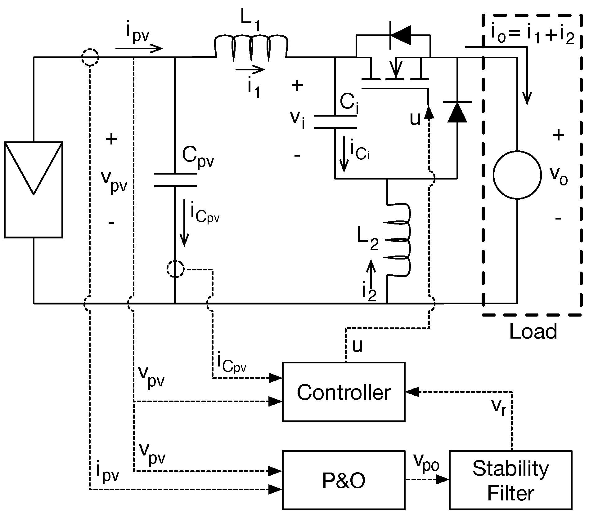
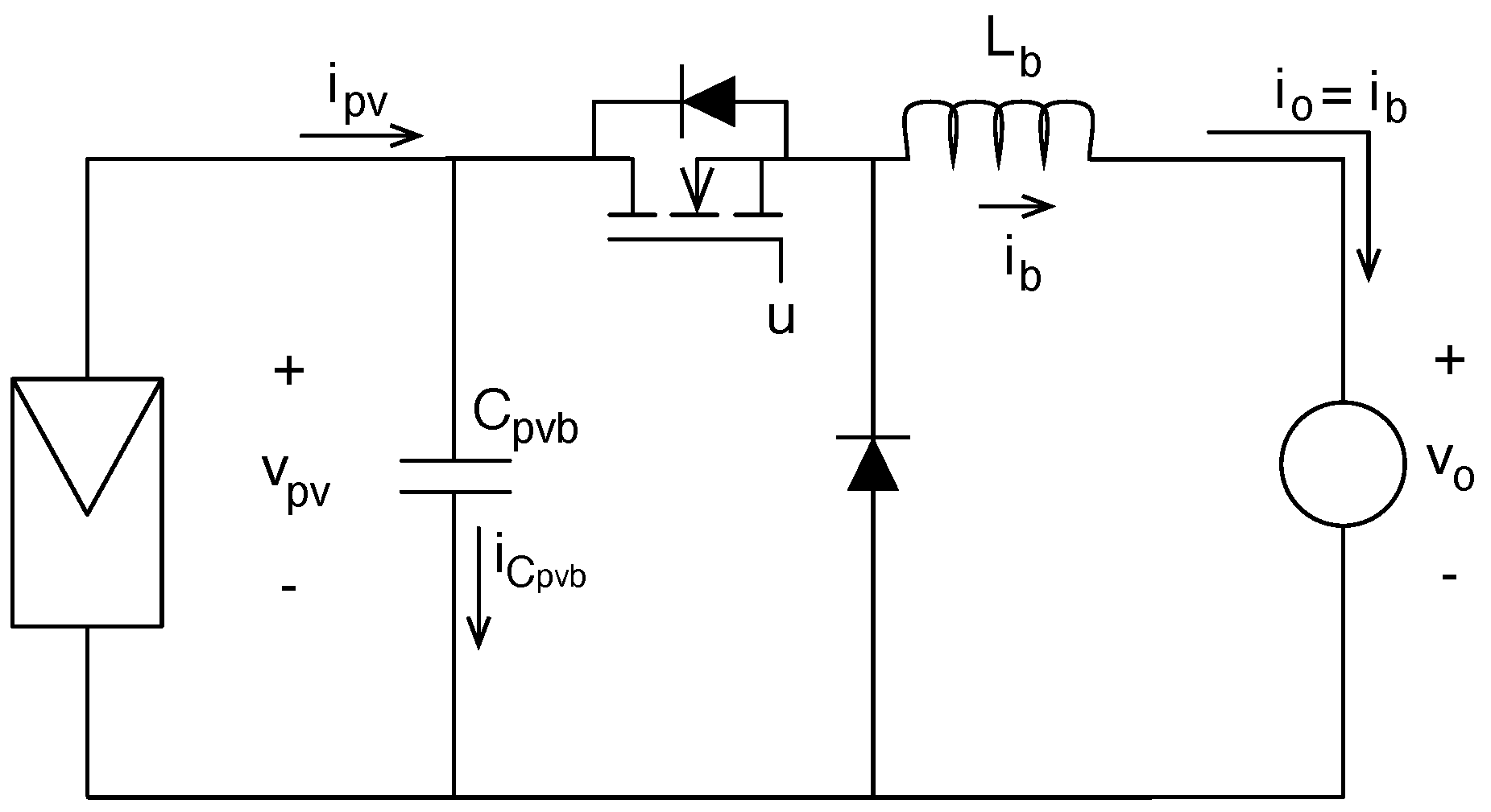
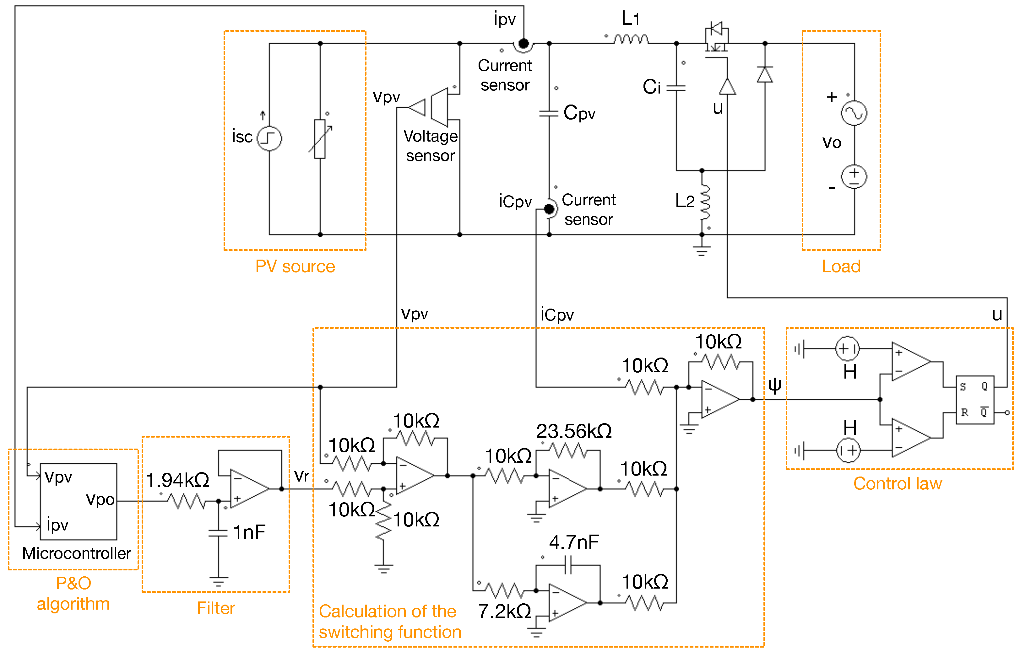
The proposed PV system based on the continuous input/output current (CIOC) buck converter is depicted in
Figure 1. Such a PV system description includes the controller required to mitigate environmental and load perturbations, which is discussed in
Section 5; the algorithm to track the maximum power point (MPPT), which in this case is the perturb and observe algorithm (P&O); and a filter needed to ensure global stability, which is discussed in
Section 5.6. The load of the PV system is modeled using the voltage source
, which represents the input of an inverter. The PV source is connected at the CIOC buck converter, where the main advantage of the CIOC converter concerns the continuous input current requested to the PV source, which reduces the input capacitor
in comparison with the classical buck converter; such an advantage is demonstrated in
Section 4. In addition, the CIOC converter also provides a continuous current
to the load (inverter), thus providing a high power quality in comparison with converters with discontinuous output current.
The CIOC buck converter is formed by a MOSFET and a diode, where the control signal
u provided by the controller defines the state of those semiconductors. Moreover, the converter has two inductors (
and
), an internal capacitor (
) and an input capacitor to regulate the PV source (
). The P&O algorithm measures the PV current and voltage (
and
) to track the optimal PV voltage
, as it is described in [
46,
47]. Then, such an optimal value is processed by the stability filter to generate the controller reference
.
The following subsections describe the behavior of the PV system, based on the CIOC buck converter, in the two operation topologies generated by and , i.e., when the MOSFET is closed and open, respectively.
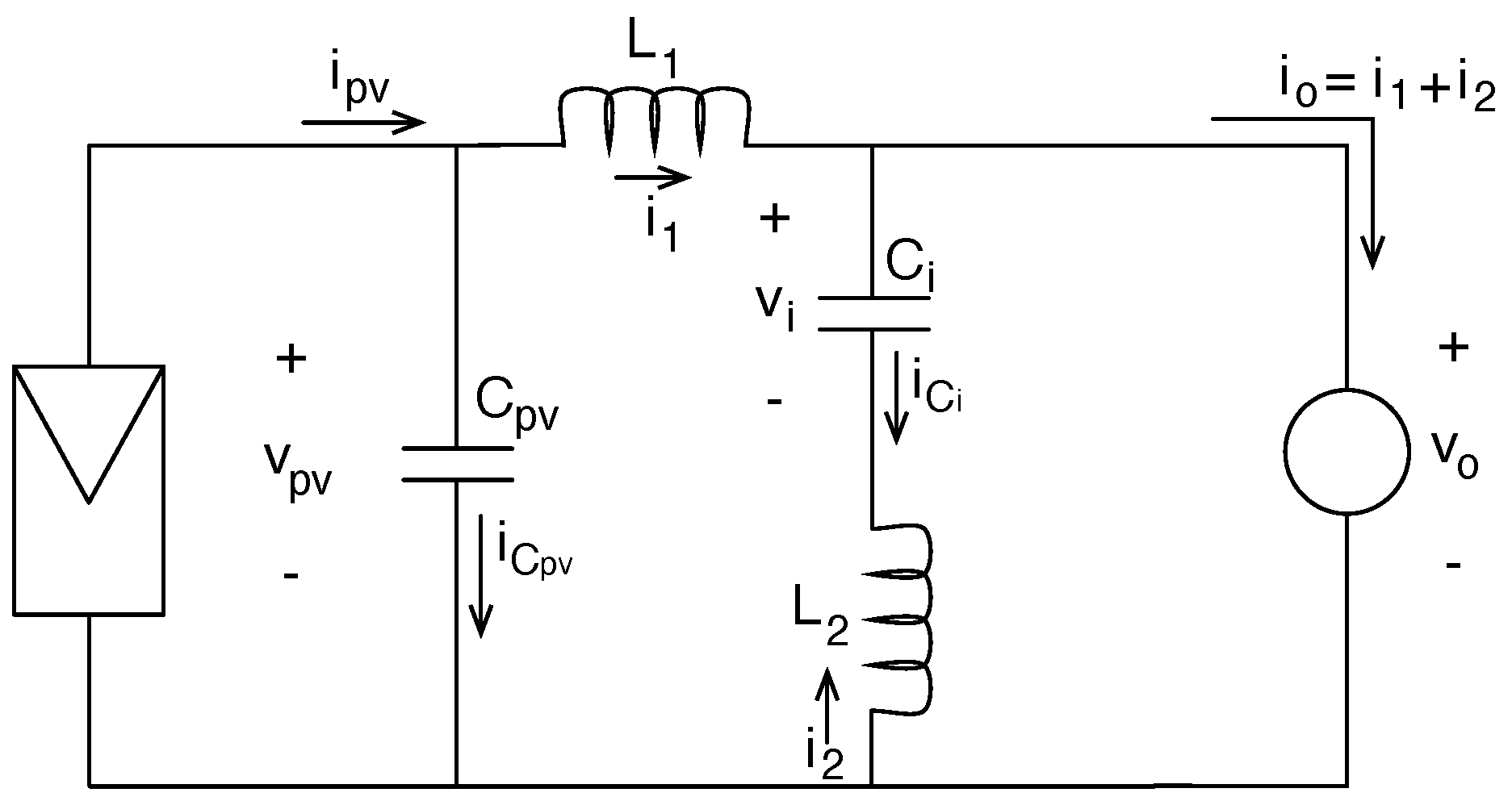
2.1. Topology 1 ()
The fist topology occurs when the control signal is
, which closes the MOSFET and opens the diode, which results in the equivalent circuit reported in
Figure 2. The topology shows that the input current of the CIOC buck converter is equal to the current of the
inductor, named
; hence, it is a continuous input current. In this topology, the internal capacitor
is discharged by the current of
(
), thus providing additional power to the load. Finally, the topology shows that the internal capacitor
provides a path connecting
and
, while the MOSFET (closed) provides a path connecting both inductors with the load. Therefore, the output current
is equal to the sum of both
and
currents, which enables the CIOC buck converter to provide a continuous current to the load.
The differential equations modeling this topology are
In addition, the MOSFET current (
) and diode voltage (
) are
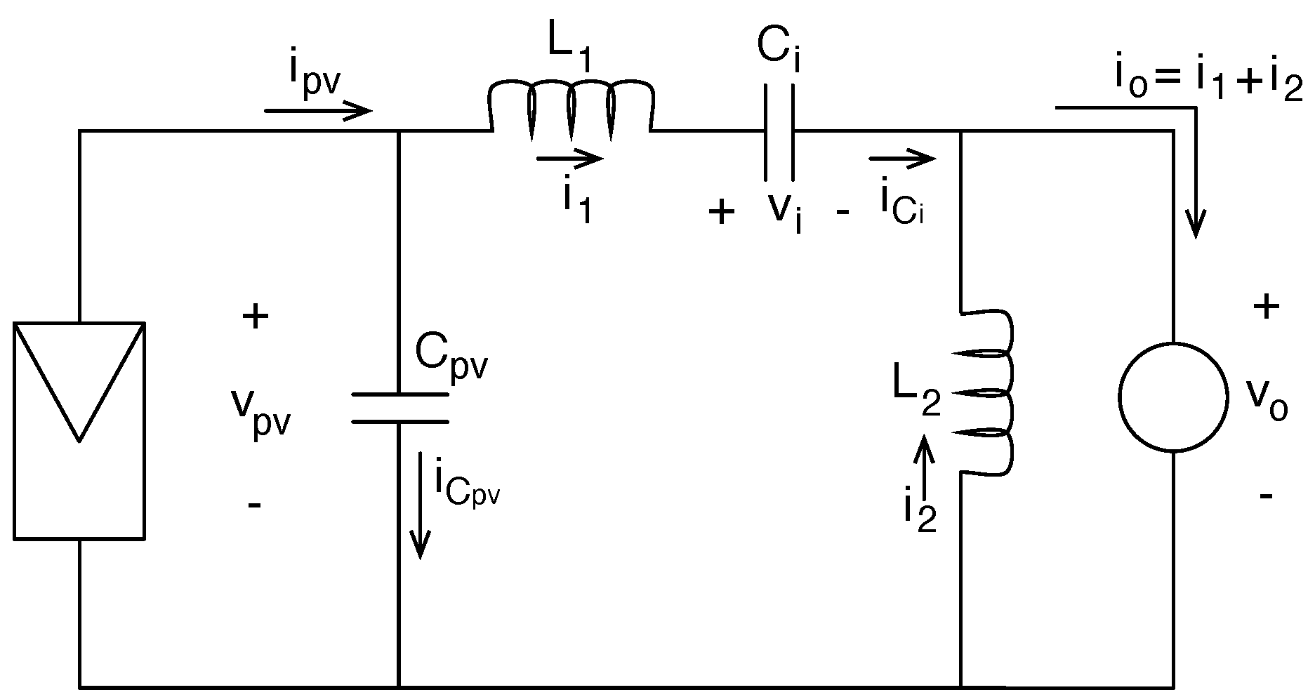
2.2. Topology 0 ()
The second topology occurs when the control signal is
, which opens the MOSFET and closes the diode. The equivalent circuit is reported in
Figure 3, which also shows that the input current of the CIOC buck converter is
. In this topology, the internal capacitor
is charged by the current of
(
), and it also provides the path connecting
and
, while the diode (closed) provides a path connecting both inductors with the load. Therefore, as in the previous topology, the output current
is continuous and equal to the sum of both
and
.
The differential equations modeling this topology are
In addition, the MOSFET voltage (
) and diode current (
) are
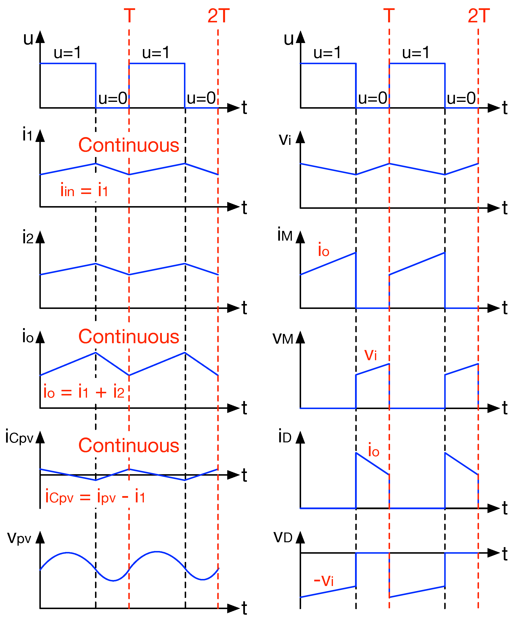
2.3. Waveforms Analysis
Figure 4 shows the waveforms of the different variables in the PV system based on the CIOC buck converter, where T is the switching period. These waveforms are constructed using the equations previously obtained in
Section 2.1 and
Section 2.2 for the two topologies occurring during the PV system operation. The waveform of the
current (
), which is the input current of the converter, confirms that the CIOC buck converter requests continuous current to the input capacitor. This is observed in the waveform of input capacitor current (
), which is also continuous, and it is centered in zero due to the charge balance principle [
29]. This characteristic ensures a smaller input capacitance requirement in comparison with converters imposing discontinuous capacitor currents, such as the classical buck structure.
The waveform of the PV voltage is obtained by integrating
, which results in a second-order ripple, as reported in [
29], due to the triangular shape of
. In contrast, the waveform of the voltage
at the intermediate capacitor is triangular, this is because such a capacitor forms a first-order filter [
29]. The current in
(
) is also triangular, and it is in phase with
. Therefore, the output current
is continuous, and it exhibits a ripple equal to the sum of both current ripples.
Finally, in topology 1 (), the output current is transferred to the load using the MOSFET, thus the MOSFET current () is a discontinuous waveform with a peak current equal to . Similarly, the output current is transferred to the load using the diode during topology 0 (); thus, the diode current () is a complementary discontinuous waveform with the same peak current. Finally, the MOSFET voltage () is equal to when , while the diode voltage () is equal to when .
In conclusion, both the input and output currents of the CIOC buck converter are continuous, which reduces the input capacitor of the PV system and provides a better power quality to the load in comparison with converters imposing discontinuous currents. This conclusion is further supported by a detailed comparison with a PV system based on a classical buck converter, which is given in
Section 4.
3. Mathematical Model of the PV System Based on the CIOC Buck Converter
The elements and controller design of the PV system based on the CIOC buck converter require mathematical models with different characteristics. The first modeling approach, named switched model, is based on the differential equations obtained in
Section 2.1 and
Section 2.2.
The switched differential equations modeling the inductor currents and capacitors voltages include the binary control signal
u, which defines the effective equations for each topology:
Similarly, the current and voltages of both the MOSFET and diode are
The previous model is useful to design nonlinear controllers with binary control signals, which is the case of the sliding-mode controller (SMC) designed in
Section 5, to ensure a stable operation of the PV system.
A second modeling approach, named averaged model, is used to design controllers with continuous control signals, such as the duty cycle
d. Moreover, the averaged model is used to analyze the closed-loop dynamics of dc/dc converters, which is the case of the closed-loop analysis performed in
Section 5.4. The averaged model is obtained by averaging the switched differential equations within the switching period
T, this taking into account that the duty cycle is the average value of the MOSFET control signal
u, as reported in Equation (
21).
Then, applying the same averaging technique for Equations (
13) to (
16) results in the following averaged differential equations:
Applying the same averaging technique for (
17) to (
20) results in the averaged equations for the currents and voltages of both the MOSFET and diode:
The third modeling approach consists in obtaining the steady-state values of the inductors currents, capacitors voltages, and duty cycle. This approach is useful to design the passive elements of the PV system and to select the MOSFET and diode according the current and voltage stresses. The steady-state equations are calculated by considering the averaged differential equations equal to zero:
It is important to note that the duty cycle (
34) is the same one required by the classical buck converter; thus, the CIOC buck converter can be used to replace classical buck converters in PV systems.
In addition, the ripple values are also needed to design both the converter and SMC. These ripples are obtained from the differential equations for each topology given in
Section 2.1 and
Section 2.2. For example, the current ripple in
is obtained in topology 1 from (
1), as given in (
35). Similarly, the current ripple in
is obtained in the same topology as given in (
36). Taking into account that
, and that
and
are in phase, the ripple in the output current is calculated as given in (
37).
The voltage ripple of
is also calculated in topology 0 from (
9), as given in (
38). Instead, the ripple at the PV voltage is calculated using the second-order filter procedure given in [
29], where the current ripple in
is integrated and the charge balance in
is applied, thus obtaining the expression given in (
39).
4. Comparison with a PV System Based on the Classical Buck Converter
Taking into account that the proposed PV system based on the CIOC buck converter has the same duty cycle as the classical buck converter, it is a suitable candidate to reduce the input capacitor of step-down PV systems. However, the CIOC buck converter has two inductors and two capacitors; thus, it is required to compare the inductive and capacitive requirements of both buck converters to provide a selection criterion.
The scheme of a PV system based on the classical buck converter is reported in
Figure 5, where the PV source is interfaced using a capacitor which must filter the discontinuous input current generated by the MOSFET. Moreover, in the classical buck converter, the inductor current is the output current provided to the load.
The mathematical model of this PV system based on the classical buck converter is given in (
40) and (
41), where
u is the control signal of the MOSFET,
is the current in the buck inductor
, and
is the input capacitance. The current and voltage of the MOSFET are
and
, respectively, while the current and voltage of the diode are
and
, respectively.
Performing the averaging procedure and making the differential equations equal to zero leads to the steady-state relations given in (
46) and (
47). Moreover, the inductor current ripple
and PV voltage ripple
are given in (
48) and (
49), respectively.
In order to provide a fair comparison between both CIOC and classical buck converters, both converters must be designed to provide the same voltage ripple to the PV source and the same current ripple to the load (inverter). Considering both inductors of the CIOC converter are equal, thus
, the output current ripple of the PV system is given in (
50). The output ripple current in a PV system based on the classical buck converter was previously reported in (
48); to obtain the same ripple magnitude in both PV systems, the classical buck solution must have half the inductance of the CIOC converter, hence
.
However, the inductor of the classical buck converter must support a higher current in comparison with the inductors of the CIOC converter, which is concluded from (
31), (
32), and (
47). Therefore, a better measurement to compare the inductive requirements of both converters is the energy stored in the inductors: for example, for a duty cycle
, the inductor of the classical buck converter stores
, since
, as given in (
47). Taking into account that
to ensure the same output current ripple in both converters, the energy stored in the classical buck inductor becomes
. For the same duty cycle
, the energy stored in each of the CIOC inductors is
, since
, as given in (
32). Therefore, the total energy stored in both CIOC inductors is
, which is the same energy stored in the single inductor of the classical buck converter. In conclusion, both converters have the same inductive requirements (in terms of stored energy) to provide the same output current ripple.
Concerning the PV voltage ripple, making equal the ripple Equations (
39) and (
49) with
leads to the relation needed between the input capacitor of the classical buck converter
and the input capacitor of the CIOC buck converter
to obtain the same ripple:
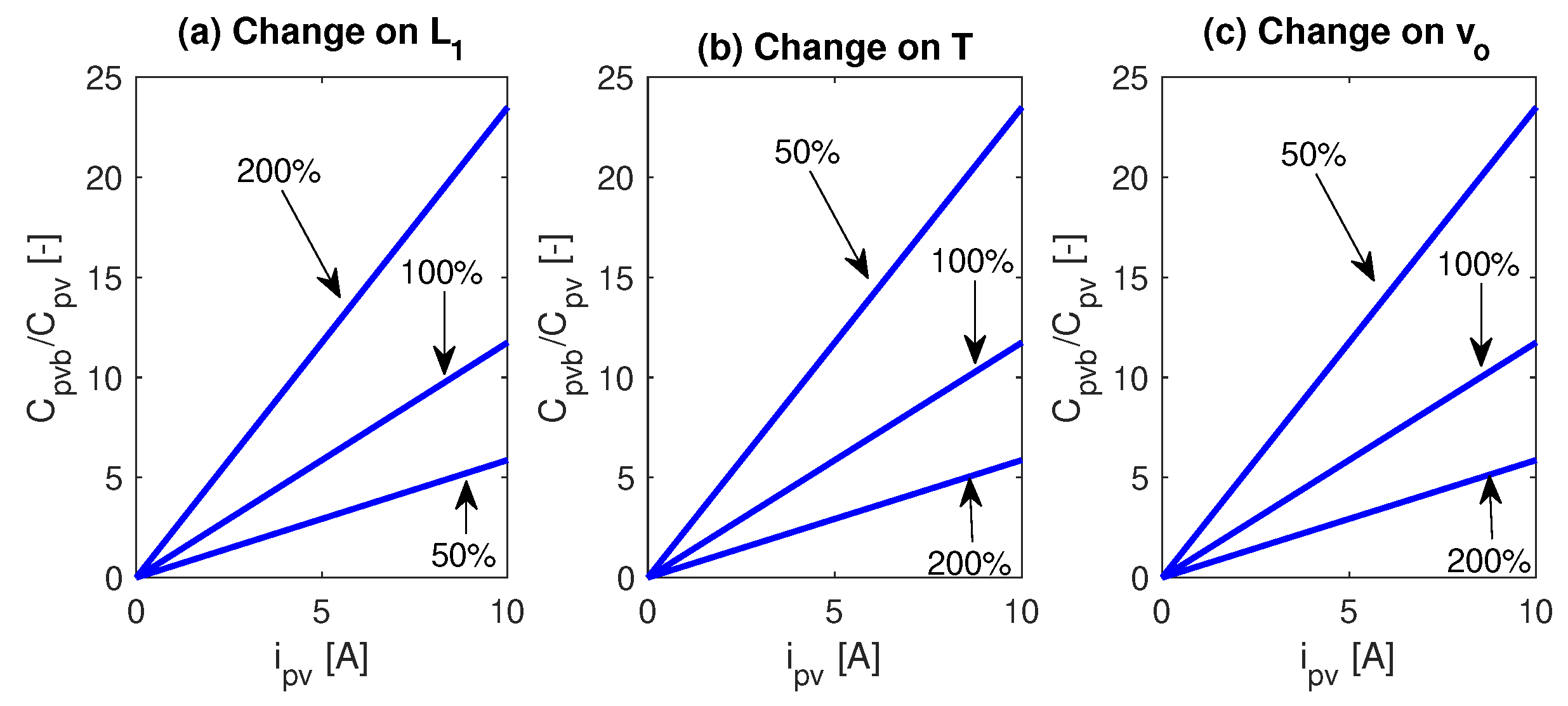
To illustrate the previous relation, an inductor of H is considered. Moreover, an output voltage for both PV system V and a switching frequency equal to kHz (s) are assumed for the comparison. Under those conditions, the classical buck converter requires an input capacitor almost 12 times higher than the CIOC converter. However, in this case, both capacitors have the same voltage, thus the energy stored in the input capacitor of the classical buck converter is 12 times higher than the energy stored in the input capacitor of the CIOC converter.
An additional comparison between both converters is provided in
Figure 6, where variations on the inductance, switching period, and output voltage are considered. These comparisons show that reducing the inductance also reduces the difference in the capacitance requirements, but at the expense of increasing the output current ripple. Similarly, increasing the switching period also reduces the difference in the capacitance requirements and increases the output current ripple. Finally, increasing the output voltage reduces the difference in the capacitance requirements, but the output voltage is defined by the load, thus it is not a freedom degree. In any case, it is important to note that in small output voltages the proposed PV system requires a much smaller input capacitor.
In conclusion, for the same PV voltage ripple condition, the CIOC PV system has a much lower capacitance requirement in comparison with a PV system based on the classical buck converter. It is noted that the CIOC PV system requires an additional intermediate capacitor
, but such a capacitor is smaller than the main capacitor
because the
current is defined by the inductor currents; this condition is illustrated in
Section 7.
6. Design Procedure and Application Example
This section synthesizes the design procedure of the proposed PV solution using an application example based on the SP500M6-96 PV panel [
53] and the commercial inverter COTEK SP-700-124 [
8], which is a 700 W inverter with a 24 V input and a single-phase ac output of 100, 110, 115, or 120 V and 50 or 60 Hz. However, both grid-connected inverters and off-grid inverters produce the inverter input oscillations at twice the output frequency. The characteristics of both the panel and pure sine wave inverter are given in
Table 1. Although a pure sine wave off-grid inverter is used in the application example, a grid-connected inverter also could be used with the CIOC. A commercial example of a grid-connected inverter is presented in [
11], where the inverter input voltage is between 19V and 33V, and the PV array maximum voltage is 250 V; moreover, this particular inverter also has an input for a battery bank with a nominal voltage of 24 V and can be connected to a grid of 230 V of 50 Hz.
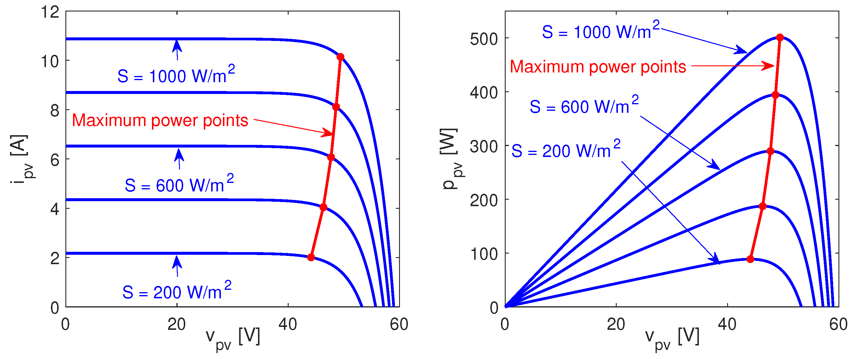
The electrical characteristics of the SP500M6-96 PV panel are presented in
Figure 8, where the current vs. voltage (I-V) and power vs. voltage (P-V) curves are observed for different irradiance (
S) conditions. The figure also shows the trajectory of the maximum power points (MPP) of the PV panel, which corresponds to the trajectory where the PV system must be operated.
The first step is to design the inductors of the CIOC converter. Since the ripple
of the output current (
37) depends on the inverse of both inductors, these inductors are designed equally to share the ripple balanced between both
and
currents, thus
. In addition, the switching frequency is limited to 100 kHz to enable the use of standard (and cheap) power MOSFET and diodes, such as CSD19538Q3A [
54] and V15P8 [
55], respectively; hence,
100 kHz. From the electrical characteristics reported in
Figure 8, it is observed that the PV source provides 88.5 W at
S = 200 W/m
, which imposes an output current of the CIOC converter (delivered to the load at 24 V) equal to 3.69 A; hence, the output current ripple at
S = 200 W/m
must be
3.69 A to ensure continuous conduction mode (CCM) in the CIOC converter for
200 W/m
. The design procedure could be performed for a lower irradiance limit, but the small current value, thus small current ripple, will introduce negligible harmonics that will not justify the increment in the inductances. Based on the previous values, Equation (
75) is used to calculate the switching frequency for different inductance values for the irradiance range 200 W/m
1000 W/m
, where the data for
S = 1000 W/m
corresponds to the MPP conditions reported in
Table 1.
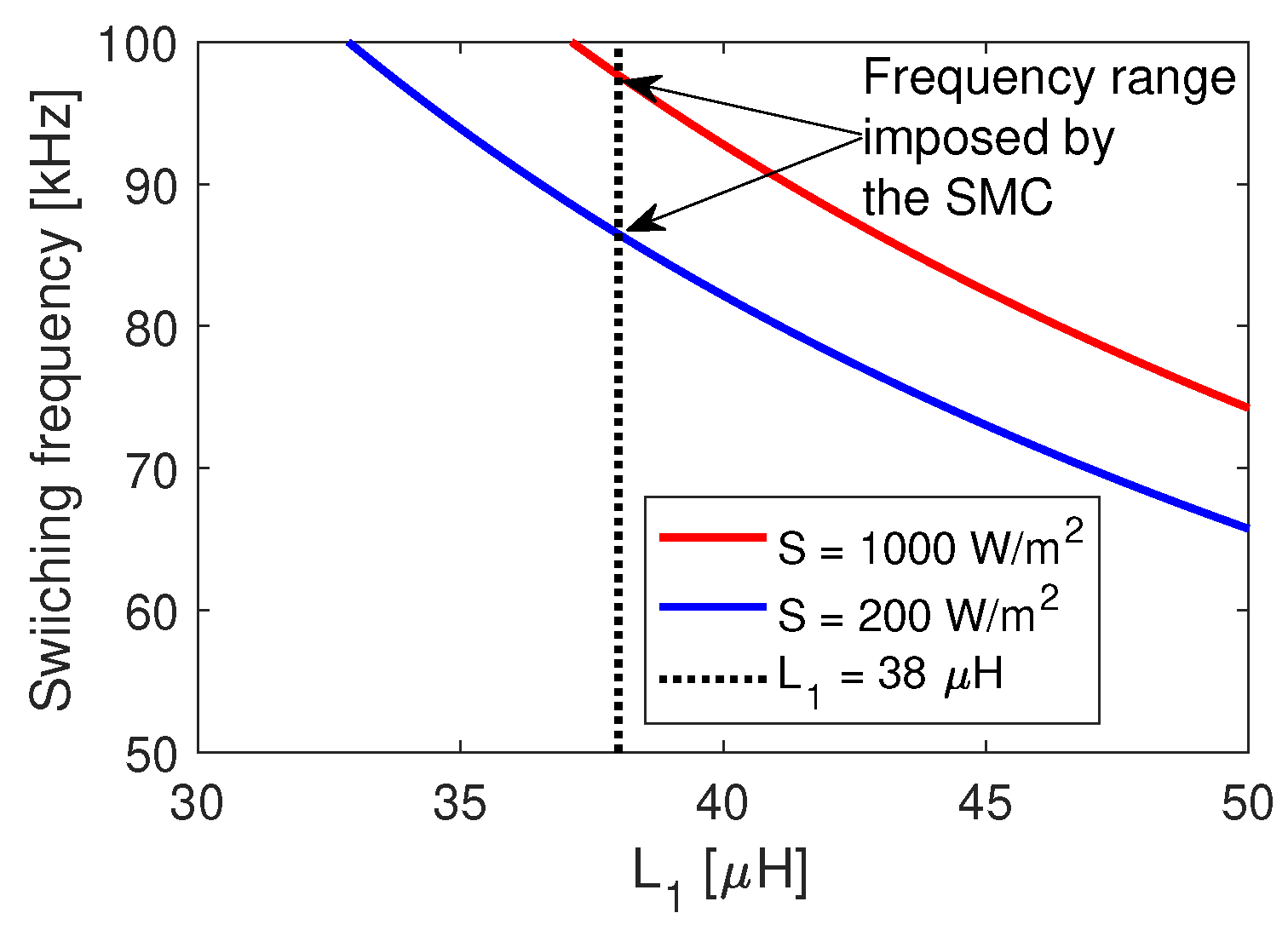
Figure 9 depicts the results of Equation (
75), where the value
=
= 38
H is selected to ensure the desired
100 kHz condition, since the Earth irradiance is always lower than 1000 W/m
.
The next step is to design the input capacitor
in agreement with the requirements of the PV system. Taking into account that the P&O algorithm has an efficiency of 99% in tracking the MPP condition [
49], the PV voltage ripple
must be lower than 1% of
. Therefore, the peak-to-peak amplitude of the PV ripple is defined as the 20% of such a 1% limit, hence
= 50.87 mV. Then, using expression (
39) and the previous value of
leads to the input capacitance value
F, where the commercial value
F is selected. Concerning the internal capacitor (
), it is designed to ensure a CCM operation for 80% of the converter conditions: taking into account that
, as given in (
30), and the peak-to-peak voltage ripple in
is defined as 20% of
, thus
= 4.94 V. Then, using Equation (
38), the internal capacitance
F is calculated, where the commercial value
F is selected.
After the power stage parameters have been designed, the following step is to calculate the appropriate parameters for the controller (SMC). The first parameter was already designed in Equation (
65), where
. The other two parameters are calculated in agreement with the requirements of the P&O algorithm, which in turn is designed as described in [
46,
47]: the perturbation amplitude is designed as the 1% of the MPP voltage, thus
= 500 mV; the perturbation period is designed as
s to provide a balance between processing requirements and tracking speed. Then, the settling time of the PV voltage is defined as 50% of the
parameter to ensure the P&O stability (
), thus
s. Using Equation (
70) and both the
and
values leads to the calculation of the parameter
= 2.36[A/V]; the remaining SMC parameter is calculated using Equation (
67) as
= 29.5[kA/ (V · s)].
The last part of the design concerns the stability filter. This application is designed to ensure global stability even under fast perturbations on the irradiance conditions, which is considered as one sun per millisecond or
= 1000 W/(m
ms), which is translated into
= 10.87 A/ms. This irradiance perturbation corresponds to a transition from full irradiance to complete shading (or vice-versa) in one millisecond, thus covering any practical perturbation. Using Equation (
60) with the system parameters and the PV current perturbation leads to the maximum reference derivative
= 0.257V/
s accepted to ensure the SMC stability. Finally, from Equation (
78), the filter time constant is calculated as
= 1.95
s, which is less than 20% of a single switching period of the CIOC converter; thus, it has a negligible effect on the settling time. The last parameter of the PV system is the hysteresis width, which is calculated from Equation (
75) as
H = 1.67 A.
Table 2 summarizes the parameters of this application example used to illustrate the proposed design process.
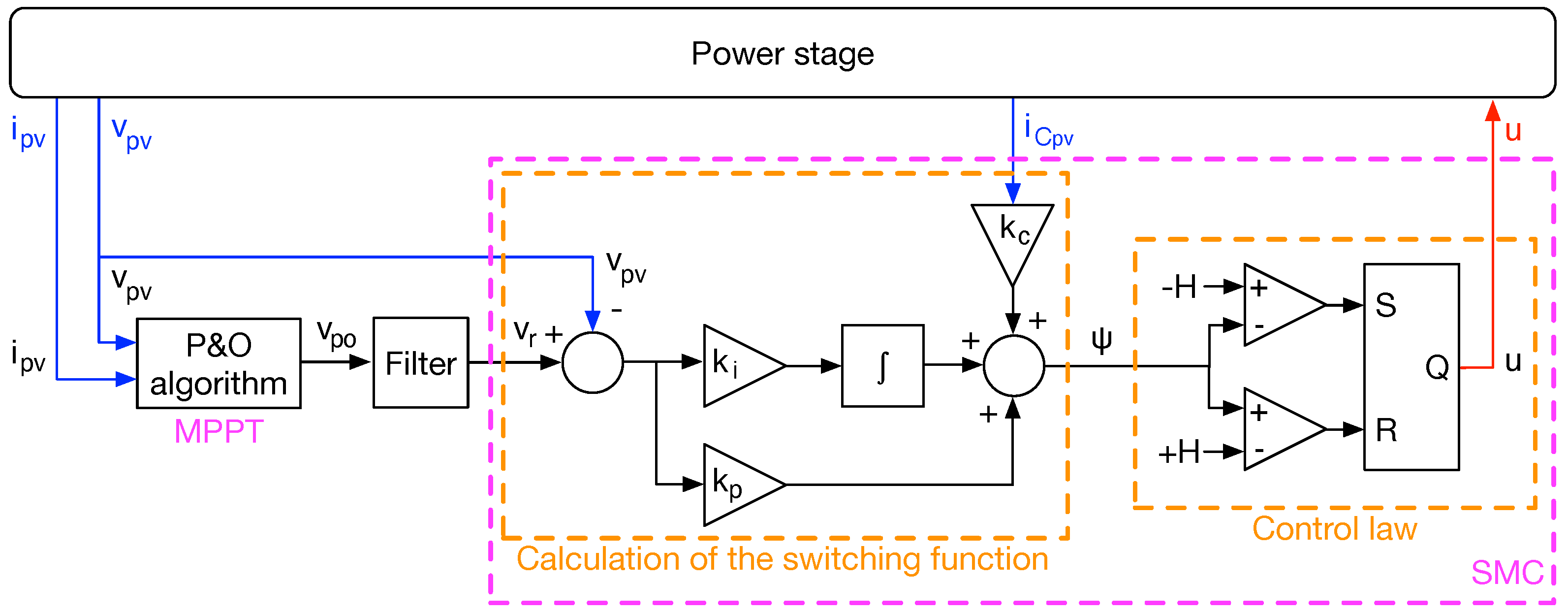
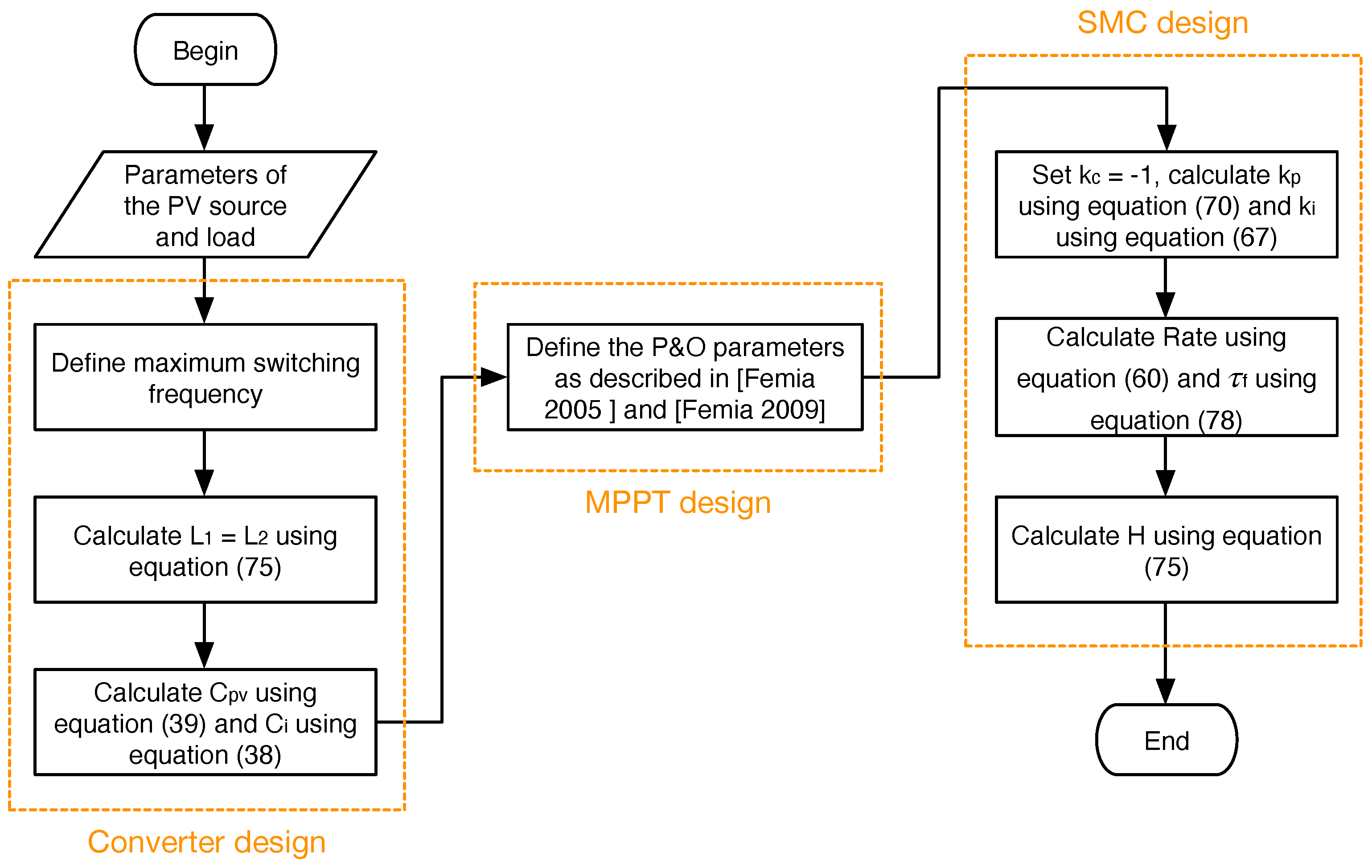
Finally,
Figure 10 synthesizes the proposed design process for the PV system based on the CIOC converter: the first part describes the converter design based on both the source and load characteristics, the second part concerns the MPPT algorithm design, and the third part is devoted to the controller (SMC) design to guarantee global stability.
7. Circuital Implementation and Simulations
The circuital implementation of the complete PV system based on the CIOC converter and the SMC was performed in the power electronics simulator PSIM [
56]. Such a commercial power electronics simulator takes into account the nonlinear and switched behavior of both the MOSFET and diode, provides realistic models for operational amplifiers and flip-flops, and also enables the emulation of microcontrollers using ANSI C code.
Figure 11 shows the proposed PV system implemented in the schematic editor of PSIM.
The PV source is implemented using the ideal single-diode model reported in [
25], where the model equation is
, and the parameters values for the SP500M6-96 PV panel are
A = 642.9 nA and
B = 0.2823 V
. The load is represented by a series connection of a DC source, which represents the average voltage imposed by the inverter, as well as a sinusoidal component at double the output frequency, which models the voltage oscillation at double of the output frequency caused by the ac connection of a single-phase inverter. The amplitude of such a low-frequency oscillation was discussed in [
57], and the mathematical analyses provided in such a work lead to expression (
79), where
is the output frequency,
is the capacitor at the input of the inverter, and
is the average voltage imposed by the inverter at the output of the CIOC converter. For the PV source and inverter parameters given in
Table 1, a capacitor
= 5.7 mF will produce a voltage oscillation between 21.6 V and 26.4 V, which fits the input voltage range required by the COTEK SP-700-224 inverter to properly operate (see
Table 1). Thus, the maximum amplitude of the load voltage perturbations is equal to 20% of the nominal value (
).
The parameters of the CIOC converter are the same ones designed in the previous section and reported in
Table 2. However, the circuit of
Figure 11 includes one voltage sensor to measure the PV voltage, which is needed to process both the P&O algorithm and the calculation of the switching function. In addition, two current sensors are also added: the first one measures the PV current, which is needed to process the P&O algorithm, and the second one measures the input capacitor current, which is needed for the calculation of the switching function.
The circuital implementation of the control stage is divided into four parts. First, the P&O algorithm is coded using the algorithm reported in [
49], which is implemented with a C-block inside PSIM to emulate a microcontroller. The second part implements the stability filter using an operational amplifier, and the third part performs the calculation of the switching function with circuits based on operational amplifiers. Finally, the fourth part implements the control law using two comparators and an SR flip-flop.
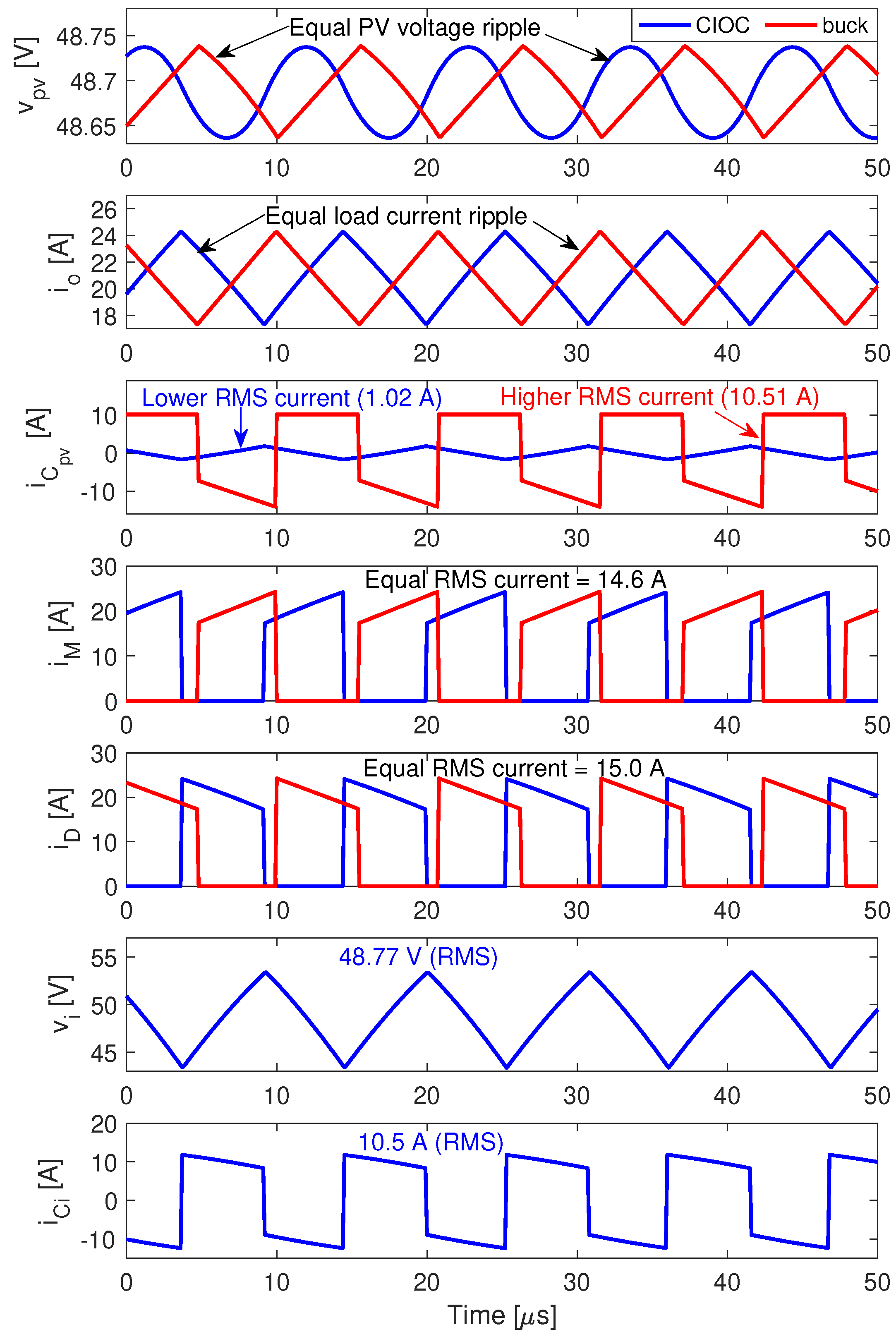
The first simulation compares the operation of the designed PV system based on the CIOC converter with a PV system based on the classical buck converter. The design of the buck PV system was discussed in
Section 4, where the buck inductor and capacitor needed to match the PV voltage, and the output current ripples of the CIOC solution are
H and
F, respectively.
Figure 12 shows the comparison of the PV systems based on both the CIOC and the classical buck converters, where both solutions introduce the same PV voltage ripple (top traces), thus fulfilling the requirements of the MPPT algorithm. Moreover, both solutions also introduce the same current ripple into the load (second traces of
Figure 12), hence providing the same power quality. However, the PV system based on the classical buck converter requires an input capacitor 11.7 times bigger than the capacitive requirement of the CIOC converter (the buck converter stores 11.7 times more energy), which introduces reliability problems, since bigger capacitances have higher failure rates [
58]. This high capacitive condition of the buck converter is caused by the discontinuous input (MOSFET) current that must be filtered in the input capacitor: the current at the input capacitor
is discontinuous for the buck-based PV system, which in this example corresponds to an RMS current equal to 10.51 A; instead, the CIOC input capacitor has a continuous current (
), thus the input capacitor must filter much lower current harmonics (RMS current equal to 1.01 A). Such a condition is confirmed in the third traces of
Figure 12. Finally, despite the inductors of the CIOC converter having higher inductance, the current processed by these inductors is much lower, and the total energy stored in the inductors of the CIOC converter is the same energy stored in the single inductor of the buck converter; thus, the inductive requirements are equivalent, as it was demonstrated in
Section 4.
Figure 12 also confirms the correct
,
, and
design: the PV voltage ripple is
mV, which is lower than the design limit calculated in
Section 6 (
mV). Similarly,
Figure 12 shows that the output current ripple is equal to
A, which is in agreement with the value predicted with Equation (
50). In addition, the switching frequency in this steady-state condition is
kHz, thus fulfilling the design criterion imposed in
Section 6 (
kHz). It must be noted that the switching frequency will never be higher than
kHz, hence the maximum switching losses can be estimated with such a limit frequency. In fact, the simulation reports that the switching frequency of both the CIOC and buck PV systems is the same, which is confirmed by the waveforms of the MOSFET and diode currents (
and
, respectively). Since both PV systems operate with the same switching frequency under steady-state conditions (
kHz), the waveforms of the MOSFETs’ and diodes’ currents are the same, just displaced in time. This is further verified by calculating the RMS currents of the MOSFETs and diodes in both PV systems, obtaining the same value. Finally, taking into account that the MOSFET and diode waveforms are equal in both PV systems, the switching losses are thus also the same; for the example in
Figure 12, these losses are, on average,
W per period considering a MOSFET on resistor equal to 4.8 m
, which corresponds to 0.3% of the generated power (
W).
Figure 12 also shows the voltage and current on the intermediate capacitor
of the CIOC PV system, named
and
, respectively. Such a
capacitor was designed to ensure a small peak-to-peak ripple in
equal to 20% of the steady-state value, resulting in the small capacitor of
F reported in
Table 2. Therefore, the capacitive storage requirements of the CIOC are not significantly increased by
, since, in this example,
= 52.6
F, which is more than 10 times smaller than the capacitive requirement of the buck-based PV system.
Figure 12 shows that the current in
is discontinuous, thus producing a large RMS current that must be supported by the capacitor; nevertheless, it is possible to find commercial film capacitors that support these RMS currents [
59,
60]. In case it is needed, increasing
to acquire a non-electrolytic capacitor with higher RMS current capability will reduce the
ripple, which will increase the power range in which the inductor currents are continuous, thus not affecting the system performance.
The second set of circuit simulations concerns the validation of the mathematical model proposed in
Section 3, including the action of the SMC designed in
Section 5. This validation is performed in both frequency and time domains.
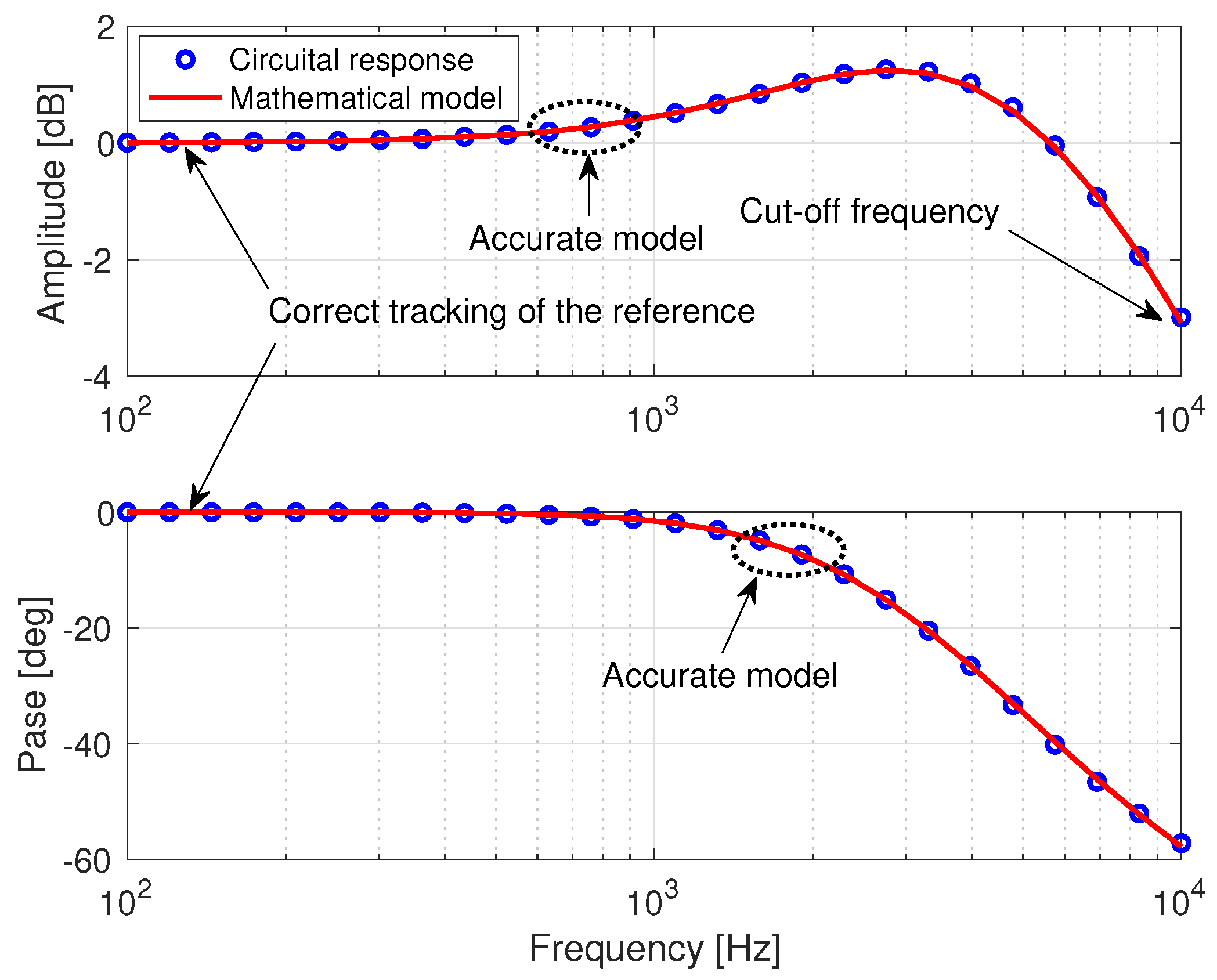
Figure 13 shows the frequency response of the closed-loop system generated by both the circuit simulation and the theoretical model previously reported in Equation (
63). These results evidence the accurate representation provided by the mathematical model proposed in this paper, since both the amplitude and phase of the frequency response are correctly predicted. Moreover, such a Bode diagram also confirms the correct tracking of the reference
, where no error or phase shift is observed up to
kHz; thus, the step-like reference of the P&O will be tracked with null steady-state error.
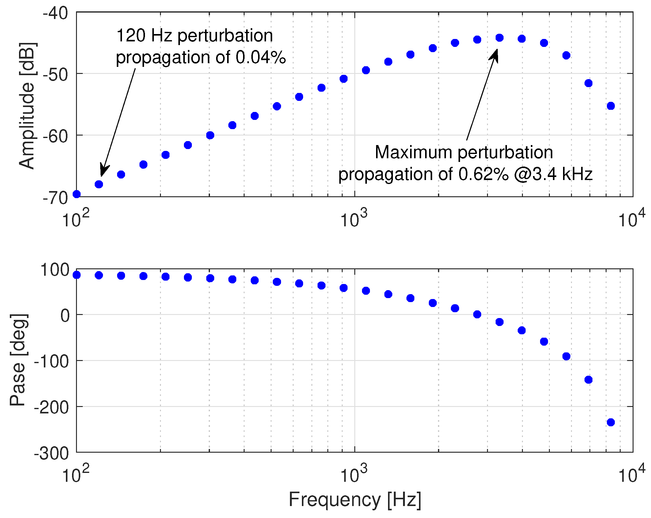
In addition, the frequency response of the closed-loop circuit to perturbations in the load voltage is investigated in
Figure 14. Such a Bode diagram confirms the correct mitigation of perturbations occurring in the load voltage, where the maximum perturbation transference is 0.62% (at
kHz). In fact, the perturbation transference at
Hz is 0.04%; thus, the voltage oscillations caused by the ac output of the inverter (load) will be satisfactorily rejected, and these oscillations will not interfere with the MPPT process.
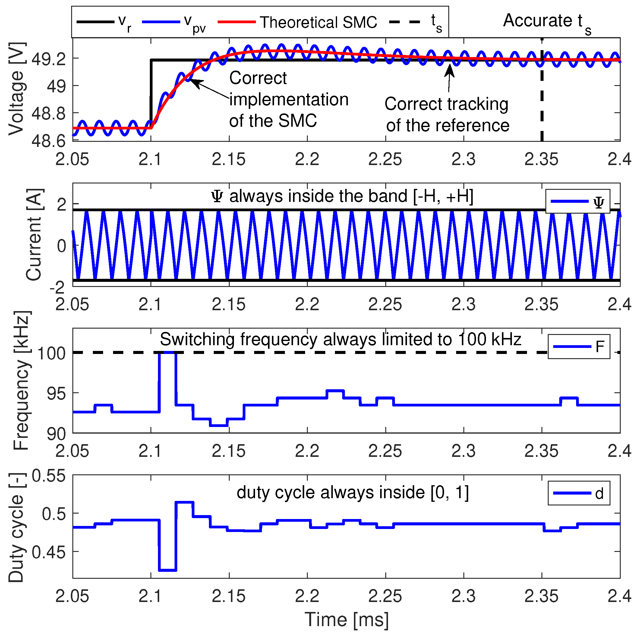
The previous frequency-based results are complemented with the evaluation of the time-domain performance reported in
Figure 15. Such a circuit simulation confirms the correct tracking of the reference provided by the SMC. Moreover, the circuital implementation of the SMC imposes the same dynamic performance predicted by the transfer function (
63), thus confirming the correct implementation of both the power stage and control system. This circuit simulation also confirms the fulfillment of both the reachability and equivalent control conditions: First, the switching function
is always trapped inside the hysteresis band (
to
), thus the reachability conditions are fulfilled; therefore, the local stability is confirmed. Second, the duty cycle is always trapped inside the physical limits (0 and 1), hence no duty cycle saturation occurs. Both conditions confirm the global stability of the PV system.
The simulation results of
Figure 15 also confirm that the switching frequency is always below the design limit (
kHz), where high switching frequencies are imposed to provide fast tracking of the reference, returning to steady switching frequencies after the transient ends. Finally, these results also confirms the accurate settling time imposed by the SMC, which fits the design value (
s). Therefore, it is confirmed that the proposed PV system (power stage and SMC) fulfills the requirements to extract the maximum power from the PV source, even with load voltage perturbations.
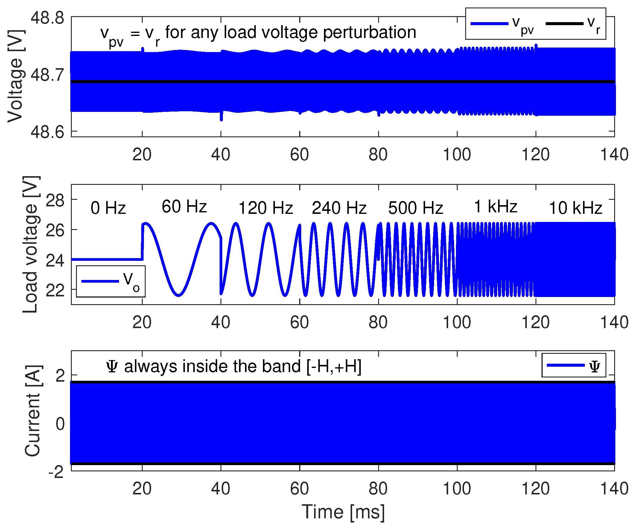
An additional simulation was conducted to evaluate the controller performance under different perturbations at the load voltage. It is clear that
Hz inverters will produce perturbations at
Hz, and
Hz inverters will produce perturbations at
Hz; however, inverter failures or nonmodeled grid behaviors could produce additional perturbations to other frequencies. Therefore, the proposed PV system was tested under load voltage perturbations at multiple frequencies:
Hz,
Hz,
Hz,
Hz,
kHz, and
kHz. The results of such a test are presented in
Figure 16, which confirm that the proposed SMC ensures the correct regulation of the PV voltage under different load voltage perturbations, thus not only the classical
Hz perturbation is compensated.
The previous conclusions are tested by implementing a circuit simulation of the complete PV system, including the P&O algorithm. Such simulation results are presented in both
Figure 17 and
Figure 18. This final test considers a changing irradiance condition with fast transients of 1000 W/(m
s) (one sun per millisecond), starting a full irradiance (
W/m
), then falling to a medium irradiance (
W/m
), and later falling to a low irradiance (
W/m
), recovering the full irradiance at the end of the profile. In addition, this test also considers a 20% voltage oscillation at
Hz perturbing the output of the CIOC converter, which emulates the connection with the commercial inverter COTEK SP-700-124 [
8].
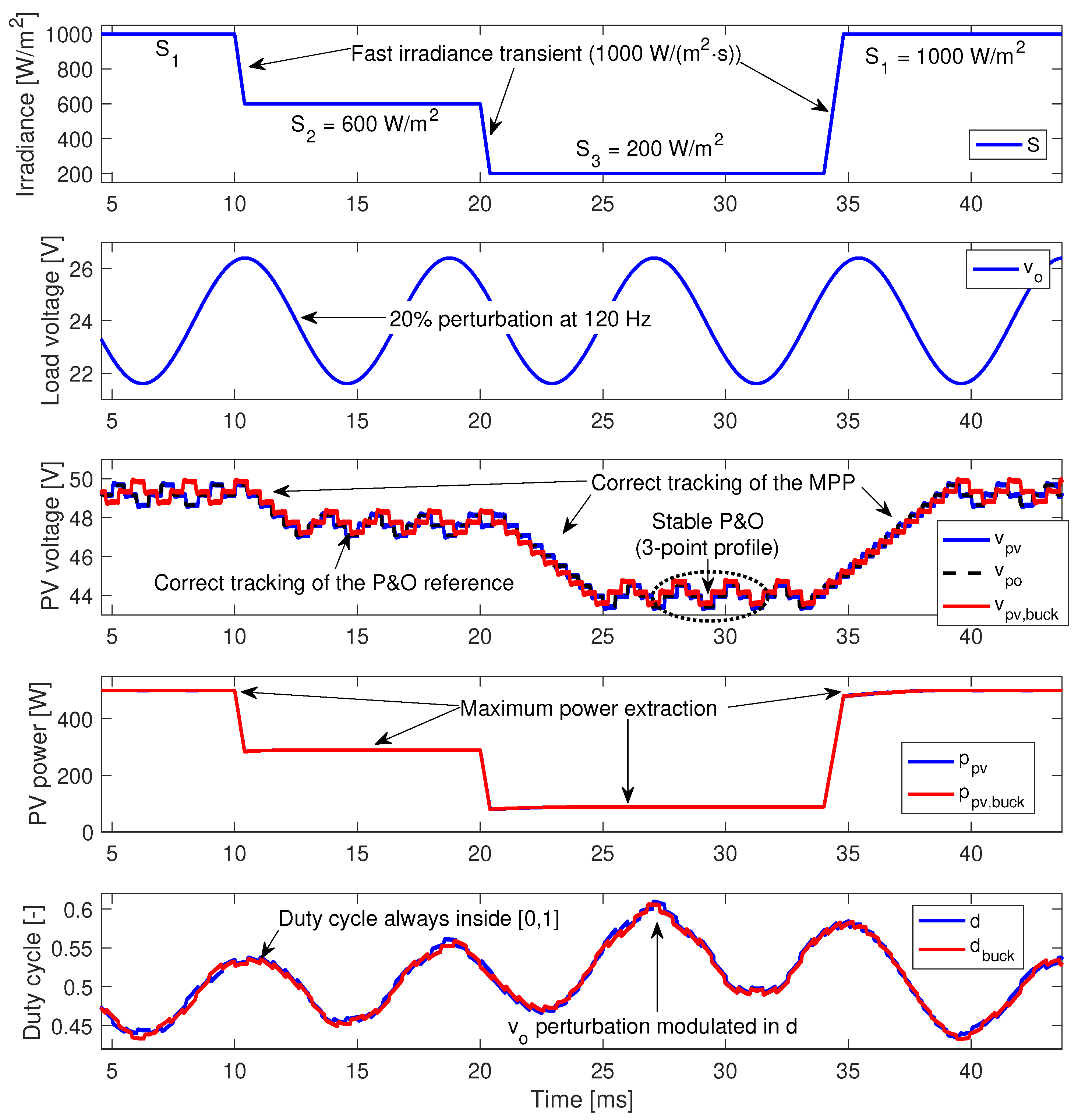
The performance of the PV voltage confirms the correct tracking of the reference provided by the P&O, which is evident since both
and
waveforms are superimposed. In addition, the PV voltage waveform also shows the three-point behavior typical of stable P&O algorithms operating at the optimal condition [
46,
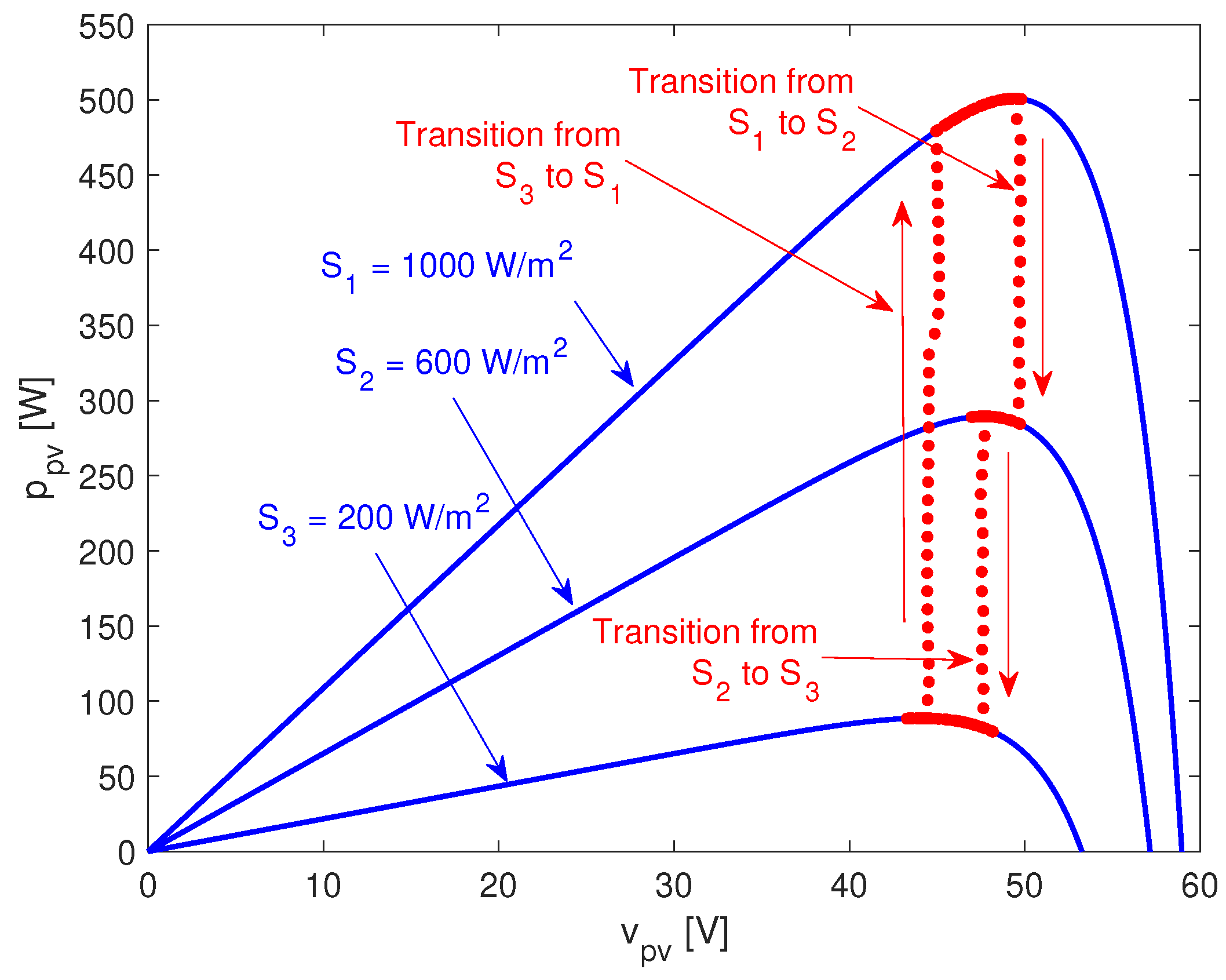
49], which ensures that the P&O algorithm reaches the maximum power points (MPP). Moreover, the tracking of the new MPP is observed in each irradiance transition. The maximum power extraction and tracking are confirmed by the trajectories reported in
Figure 18, which shows the paths taken to track each MPP. Finally, the successful operation of the PV system under load voltage oscillations is explained by the fact that these oscillations are modulated into the duty cycle, thus compensating them without saturating the duty cycle. Finally,
Figure 17 also shows the dynamic simulation of the PV system based on the buck converter previously designed for comparison purposes (red waveforms). To provide a fair comparison, such a buck-based PV system was complemented with the same P&O algorithm [
61] and with a sliding-mode controller designed as described in [
28] to provide a similar settling time. The results confirm that both the proposed CIOC and buck-based solutions provide the same PV power, which is expected since the buck converter was designed to provide the same ripples as observed in
Figure 12, thus resulting in the same duty cycle and similar voltage profiles but requiring much higher capacitive storage for the classical buck solution.
In conclusion, the circuit simulations performed in this section confirm the following conditions:
The CIOC converter was accurately designed to impose the desired current and voltage ripples to both the PV source and the load.
The CIOC converter provides the same ripples in comparison with the buck converter, requiring the same inductive energy storage but with much lower capacitive energy storage, thus improving reliability.
The SMC provides global stability to the PV system in any operating condition.
The proposed PV system, based on the CIOC converter and SMC, ensures the extraction of the maximum power, even with high perturbations in the load voltage, which is a common case when inverters are added to the PV system to form a small-power microinverter.
8. Conclusions
A low-voltage photovoltaic system that uses a continuous input/output current buck converter was proposed in this paper. The design of the converter and its control systems included the definition of the maximum switching frequency of 100 kHz and the calculation of two inductances, uH, two capacitances, uF and F, P&O algorithm parameters, mV and ms, three controller parameters , A/V, and kA/(V· s), and A, which ensures the maximum switching frequency.
The main advantage of the proposed PV system is to impose desired current and voltage ripples to both the photovoltaic source and the load with lower input capacitance requirements than the classical buck converter. For instance, in a simulated application with the SP500M6-96 PV panel and the commercial inverter COTEK SP-700-124; the imposed PV voltage ripple was mV, with an input capacitor of F and an internal capacitor of F. Moreover, the implemented P&O algorithm extracted the maximum power of the photovoltaic source, in this case W, W, and W for three different irradiance values, and the proposed sliding-mode controller provided global stability to the system in any operating condition and rejected output perturbations, including the double-frequency oscillations of Hz produced by an intended microinverter. To simulate the application example, circuit simulations, developed with the power electronics simulator PSIM, confirmed that the designed CIOC converter imposed the desired current and voltage ripple to both the PV source and the load. Moreover, the CIOC converter provided the same ripple compared with the classical buck converter, requiring the same inductive energy storage but with lower capacitive energy storage.
Despite the advantages of the proposed low-voltage photovoltaic system, some requirements were faced to operate the system satisfactorily: a complex mathematical model of the converter to design the controllers, which also requires a complex theory to be analyzed and designed, and the design of the converter is more complex than the classical buck to achieve the requirements of the PV system.
For the implementation stage, two clear disadvantages will have to be covered: a greater number of elements than the classical buck converter, reducing the reliability of the system (one more inductor), and the design and implementation of the MOSFET driver in the high-voltage side of the system.

 ,
, 


