
Machine Learning and Rules Induction in Support of Analog Amplifier Design

Abstract
:1. Introduction
2. Design Process of Analog Devices
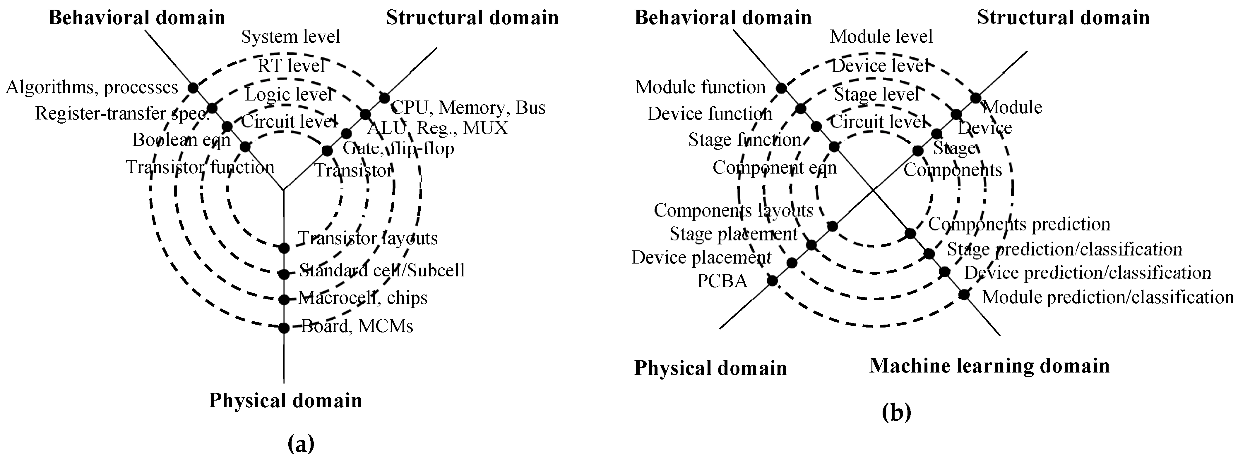
- The behavioral domain in the Gajski–Kuhn Y-chart presents the function of a given circuit without knowing the components that are included for its implementation. In this domain, the electronic circuit is seen as a “black box”, in which only its inputs and outputs are known.
- The structural domain defines how the circuit is built. It considers the circuit structure, building components and the connections between them. The structural domain provides one of the possible transformations of the behavioral description into a set of components and relationships between them, which satisfies the predefined user specification.
- The physical domain shows exactly how the circuit has to be implemented on the board layout in order to ensure the desired behavior of the circuit. The main problems here concern the component placement on the PCB and their routing, taking into account the constraints of the limited chip area, the specific features of the components and their physical geometry, the routing collisions, and congestion. Physical design is a complex task and is currently performed in several steps: macro placement, global placement, detailed placement, global routing, and detailed routing.
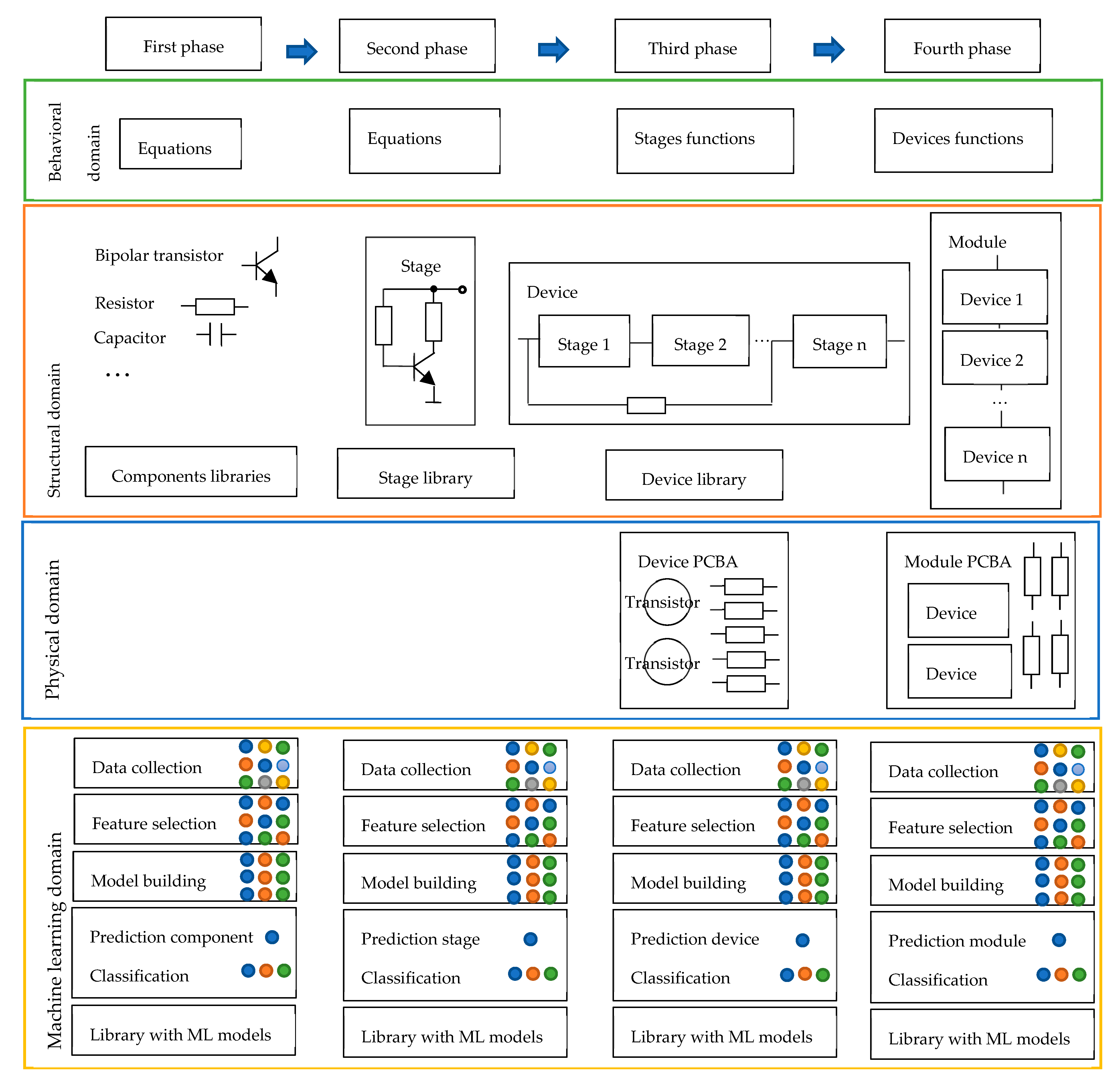
- (1)
- The first phase identifies suitable components for analog circuit creation. The common added components are transistors, resistors, capacitors, diodes, etc., which are organized in libraries. The electrical behavior of components is described with equations. The created machine learning (ML) models, which are also organized in libraries, are capable of predicting and classifying possible components for circuit implementation of a given stage.
- (2)
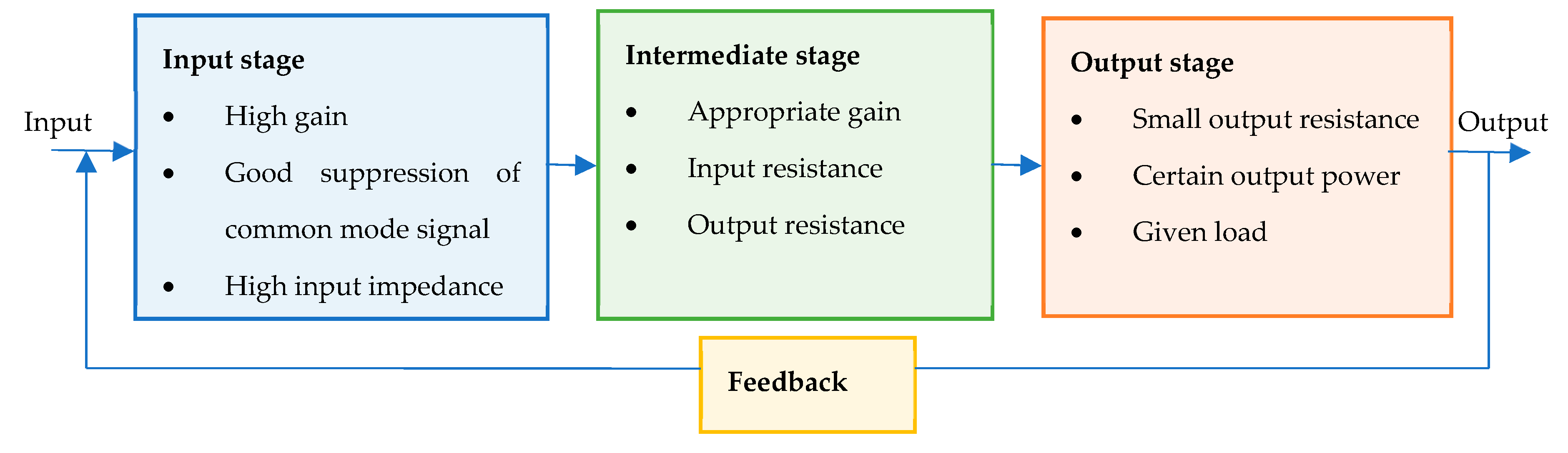
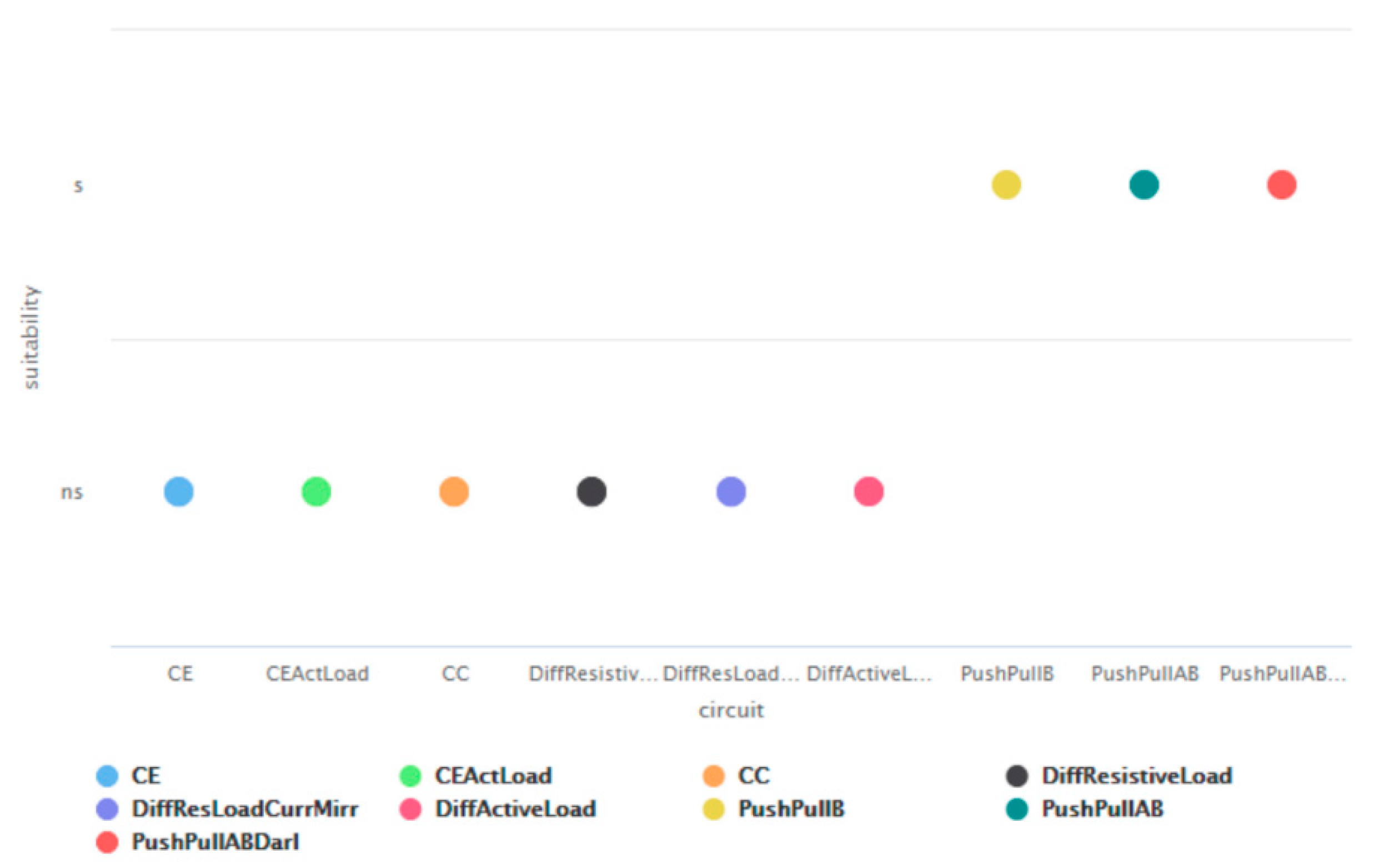
- The second phase determines the appropriate stages that can form the circuit device. In the case of amplifier design, the circuit can be built from one stage, which is called a single-stage amplifier; a circuit built from two stages is known as a two-stage amplifier; and a circuit built from more stages is known as a multi-stage amplifier. An amplifier stage includes an amplifier element (here are considered just transistors), a circuit for connecting to the signal source, a power supply circuit, a circuit for ensuring the constant current mode, and a circuit for connecting to the load. It may also contain a circuit for implementing feedback in order to improve or change the parameters and characteristics of the stage. The schematics of all stages are organized in libraries. Machine learning is used for predicting/classifying the behavior, and the structure of possible stages through equations and transfer functions, as machine learning models are placed in a library.
- (3)
- The third phase connects the identified stages forming a device. Some additional circuits may be added as common feedback or circuits for correction. The most commonly used devices form device libraries. Machine learning models predict/classify the behavior and structure of the device, in addition to its placement and routing on the PCB, taking into account the device function.
- (4)
- The fourth phase demonstrates the realization of more complex electronic products, i.e., so-called modules. One module may consist of one or several devices, which are connected to realize the predefined user specification. Some additional circuits for parameter improvement and correction can be added. Machine learning predicts/classifies the behavior and structure of modules and device placement on the PCB, considering the devices’ transfer functions and the function of the whole module.
3. Design of Analog Amplifiers
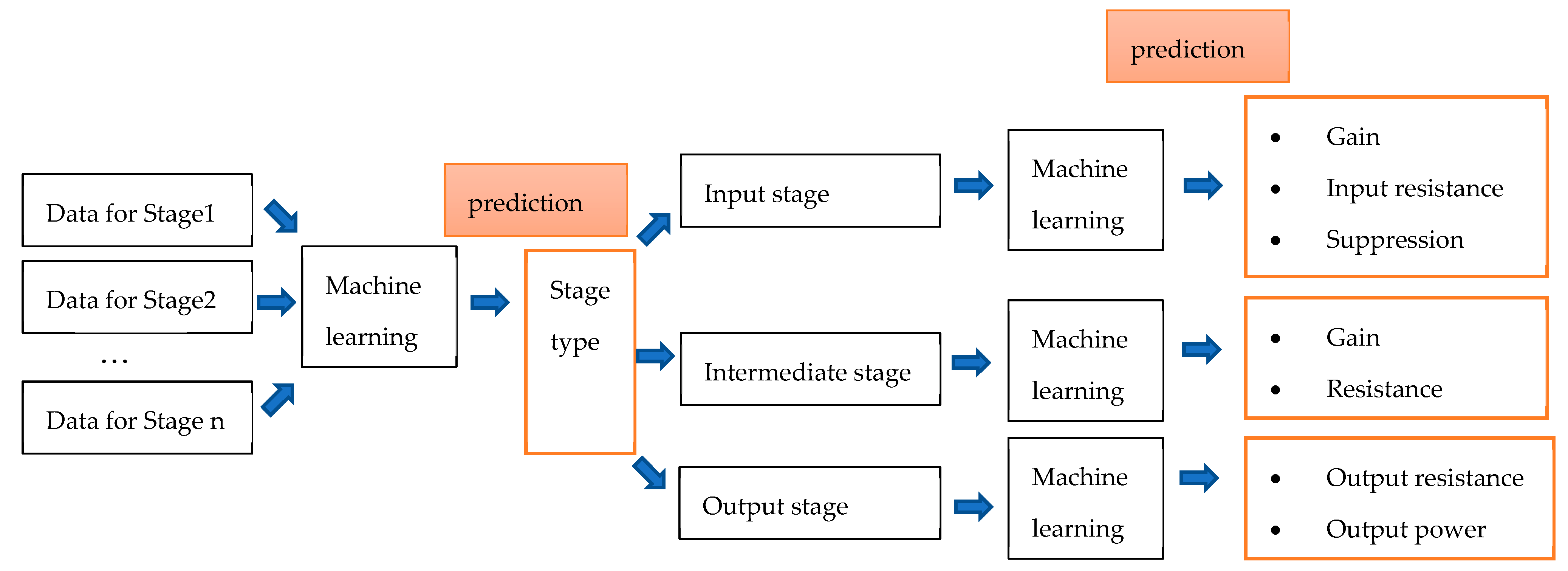
4. Proposed Method
Datasets Preparation
| Algorithm 1: Design of output stage Preliminary data: load resistance , output power , voltage supply ; choice of power transistors and their parameters, taken from datasheet specifications [32,33] |
|
| Algorithm 2: Design of intermediate stage Preliminary data: taken from datasheet specifications [34,35] |
|
| Algorithm 3: Design of input stage Preliminary data: choice of low power transistor and its parameters, taken from datasheet specification: [36] |
|
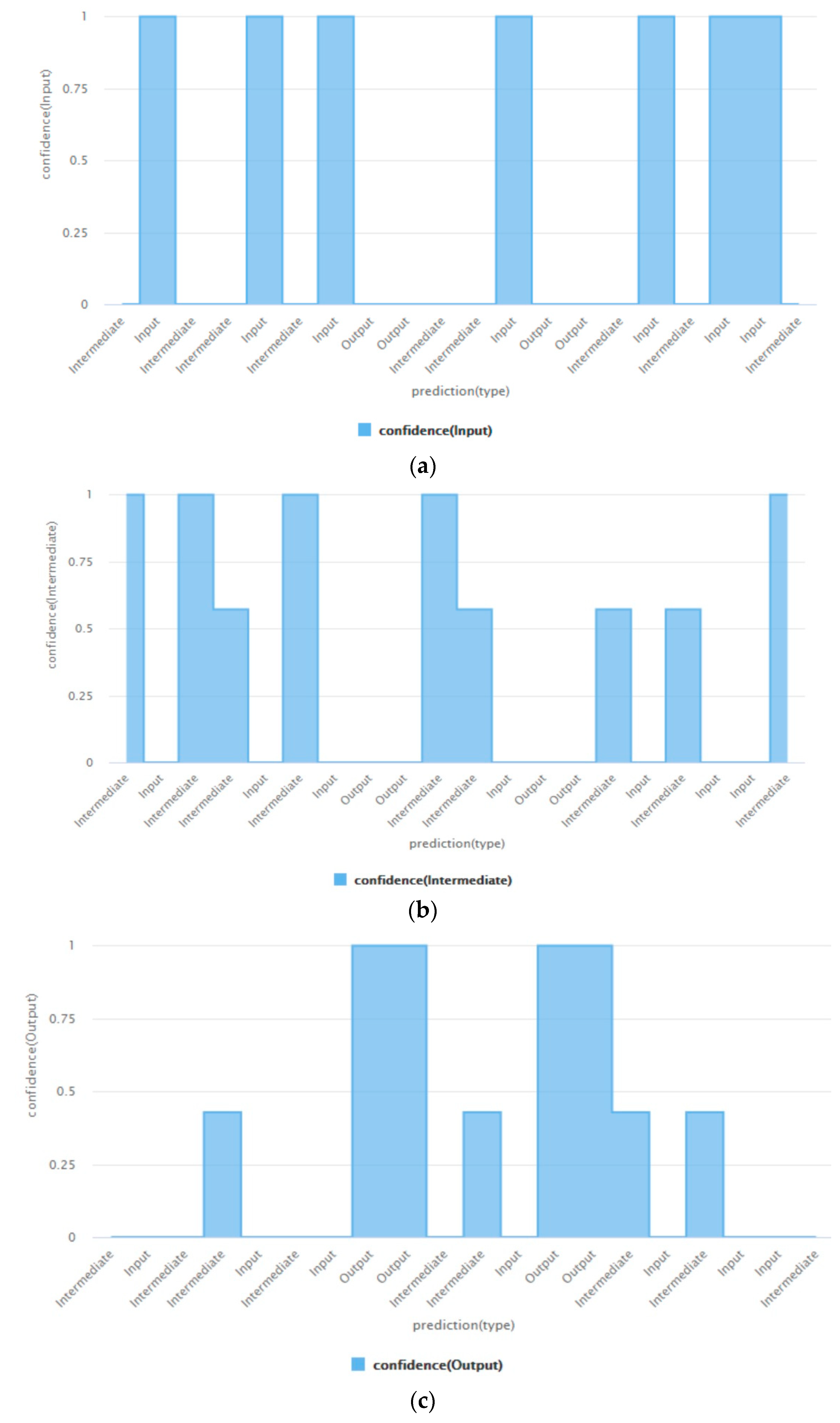
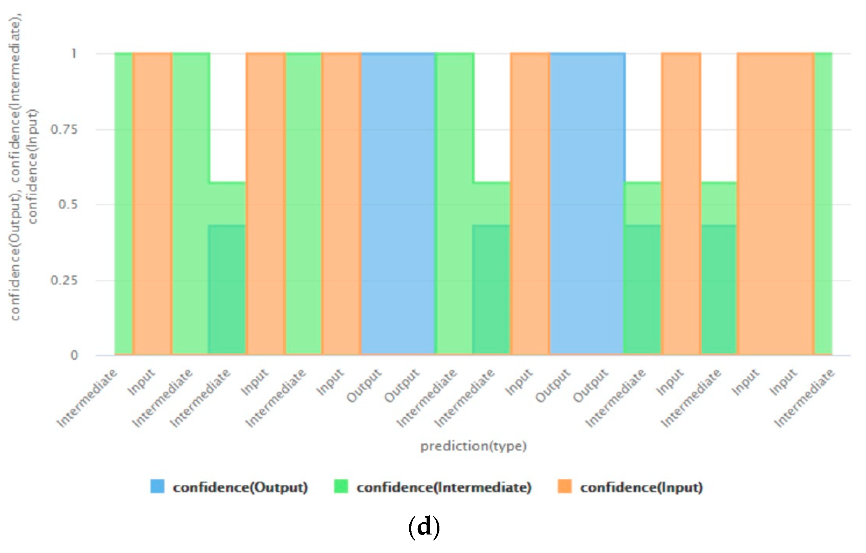
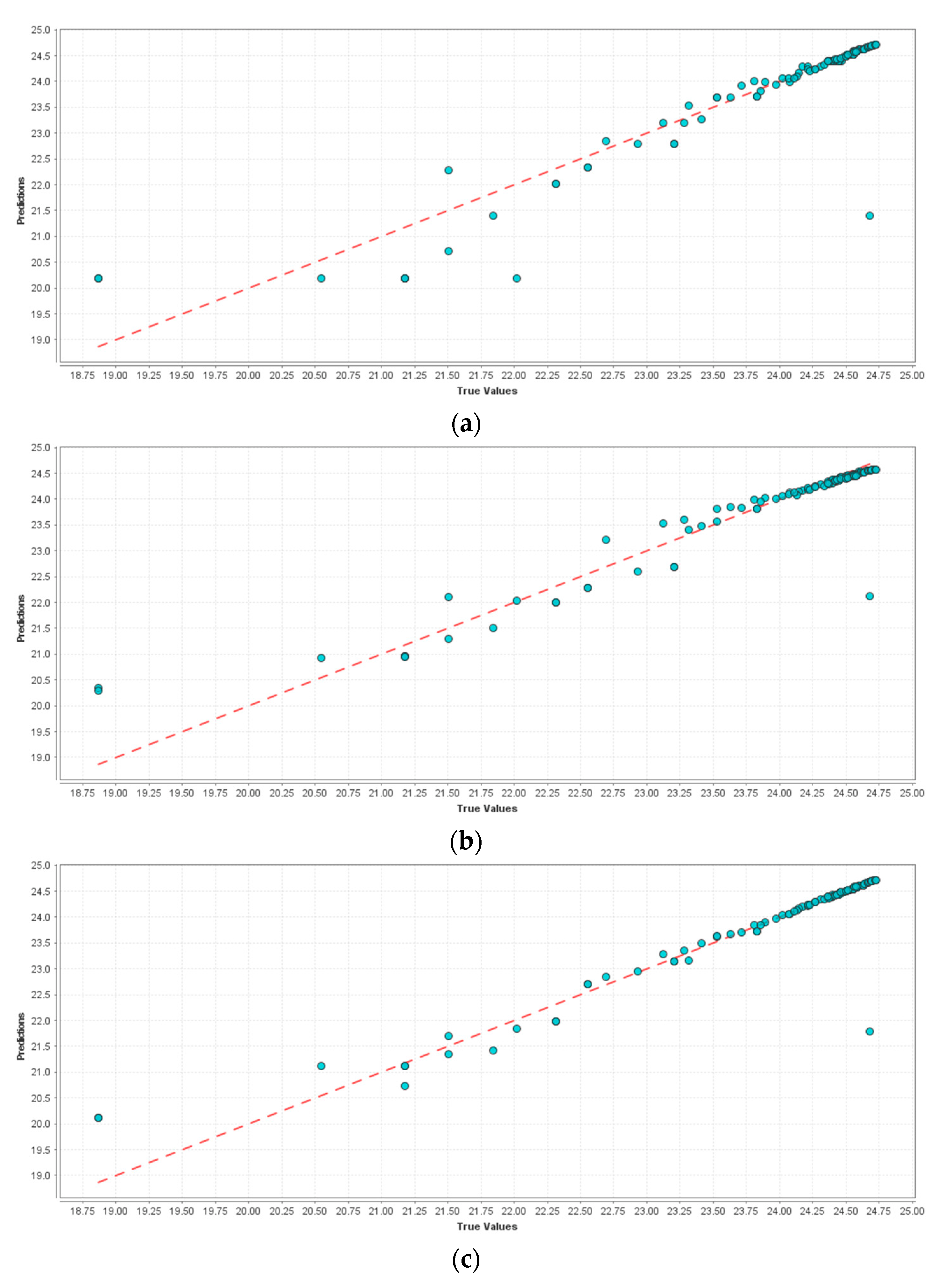
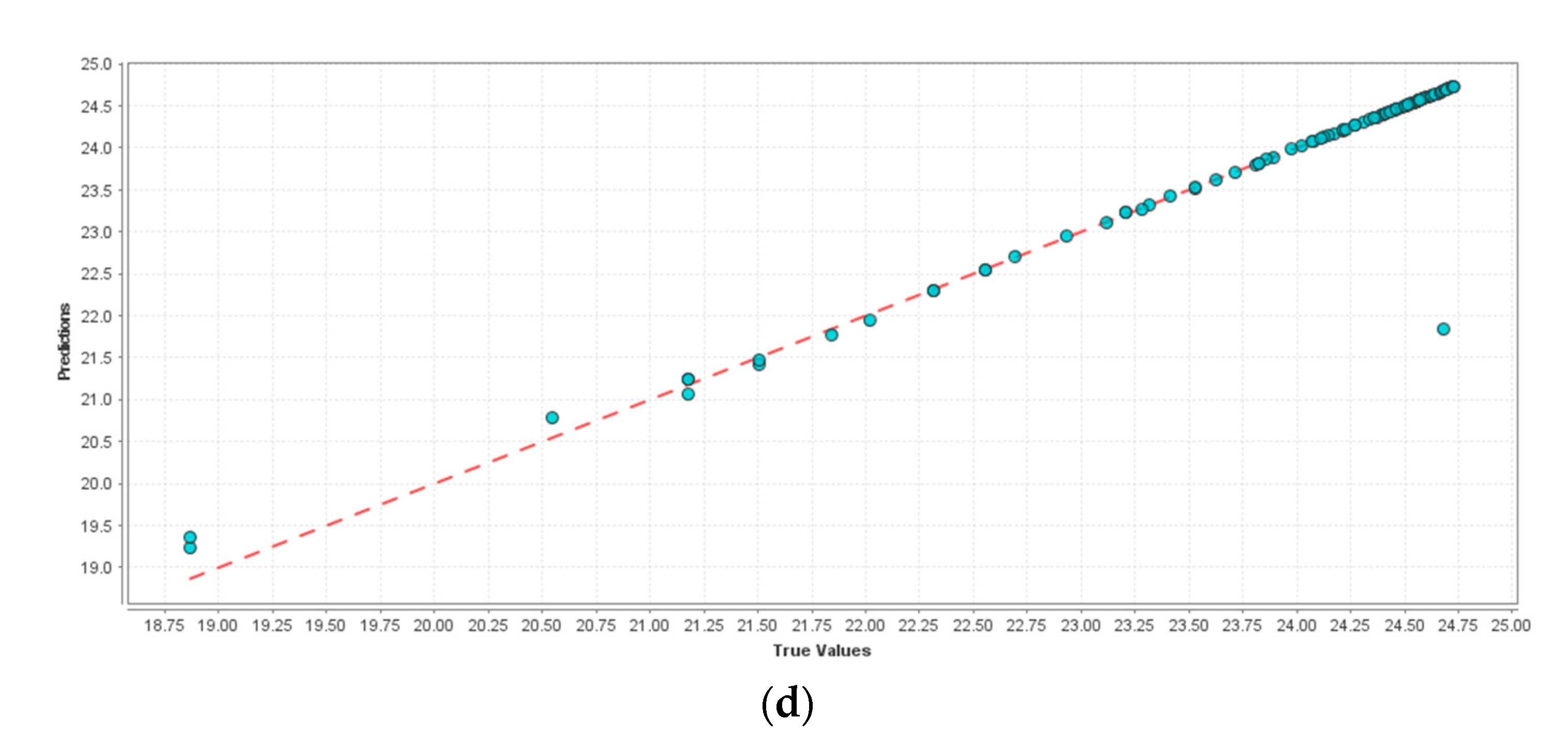
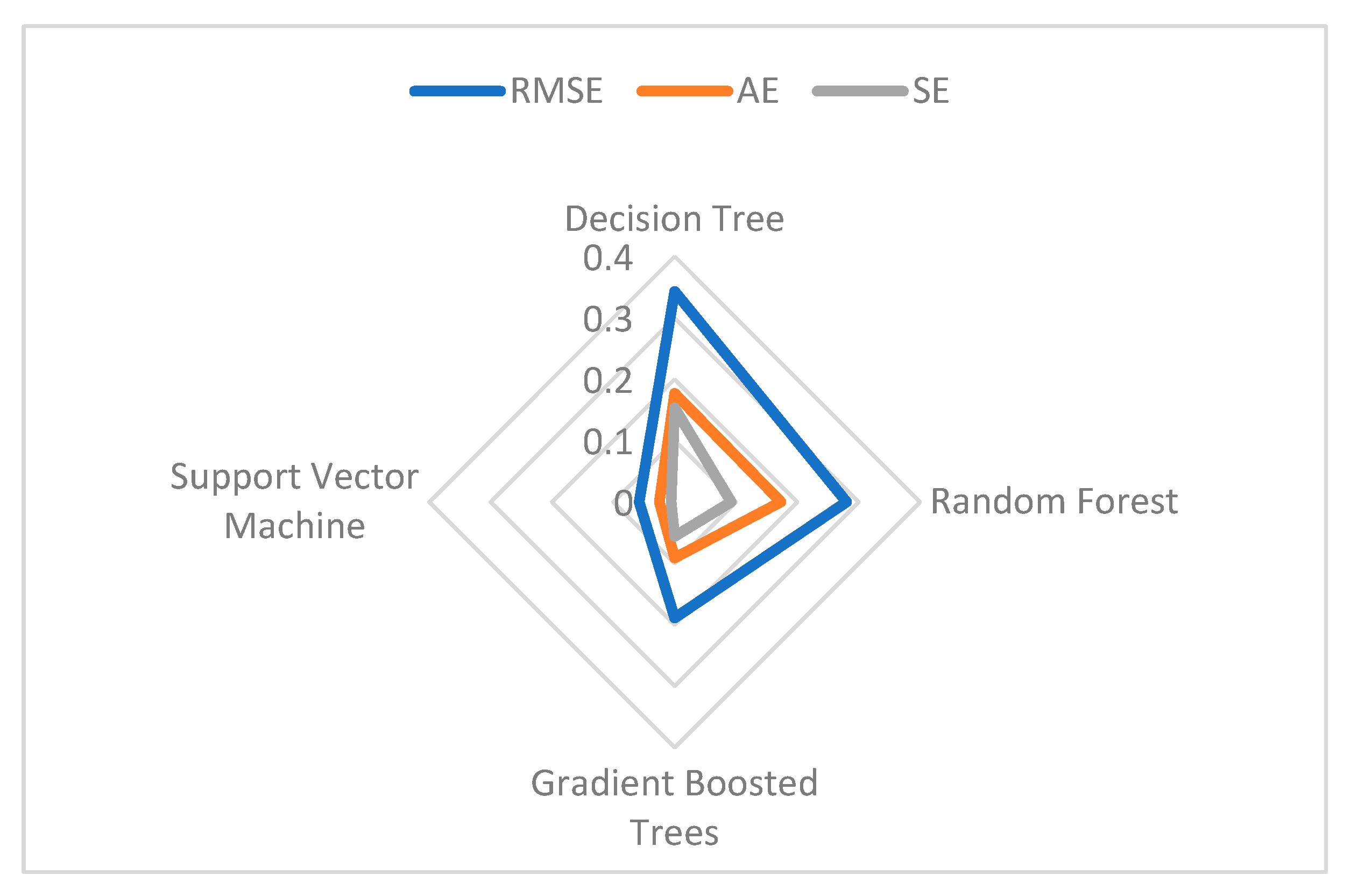
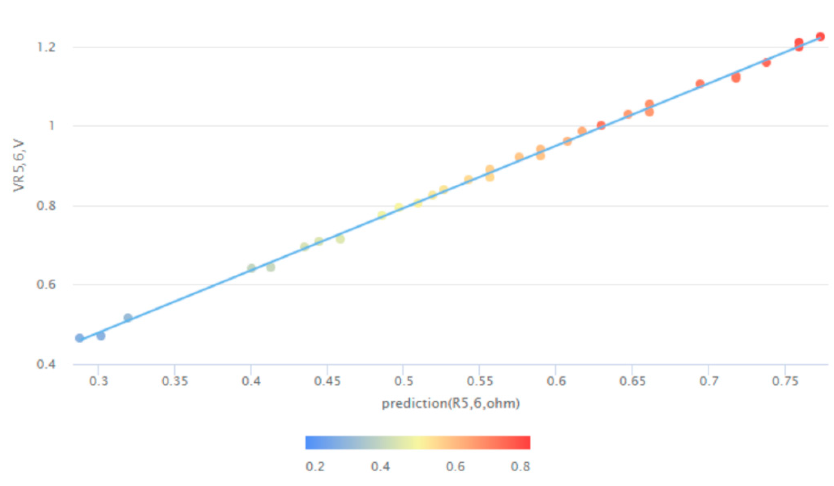
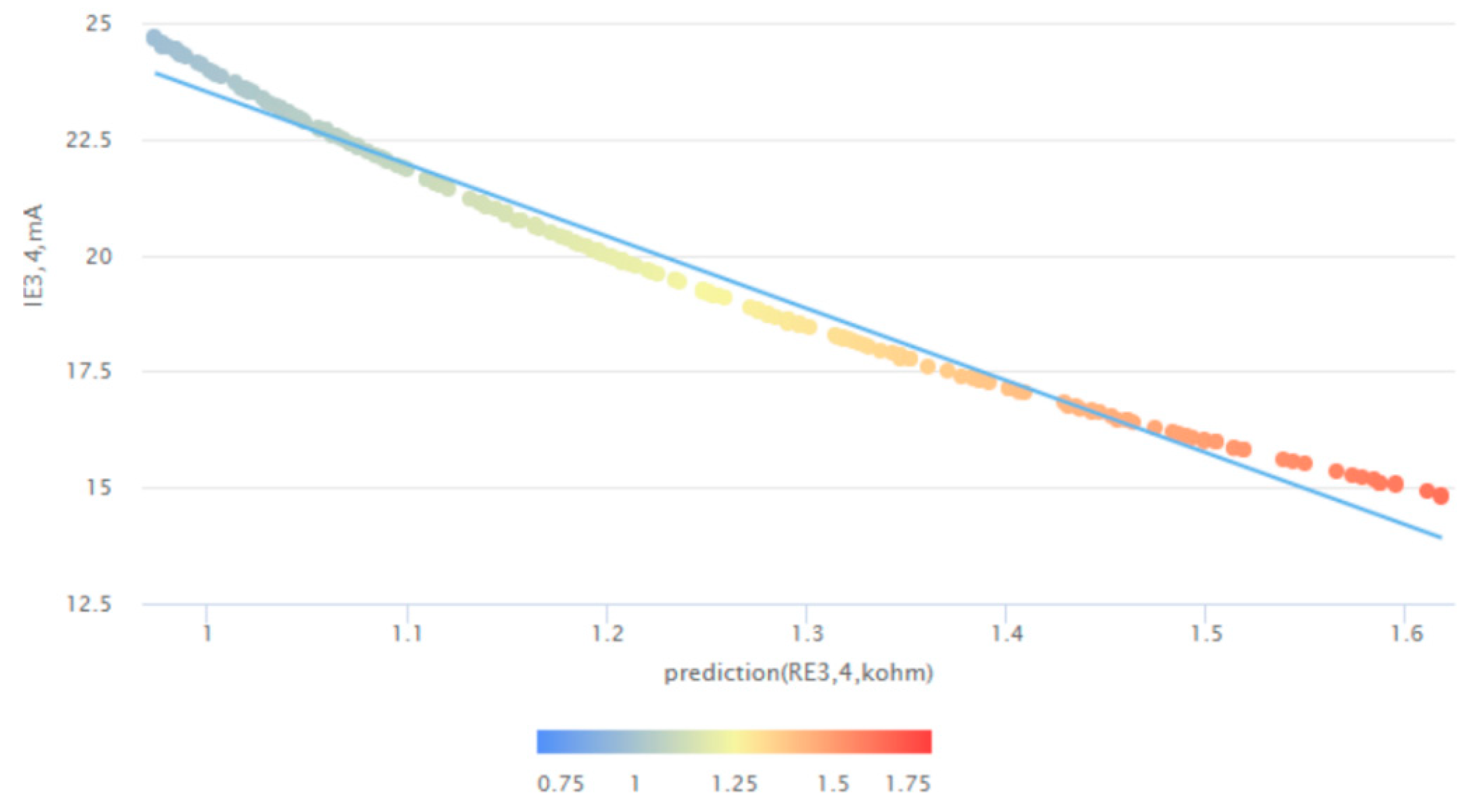
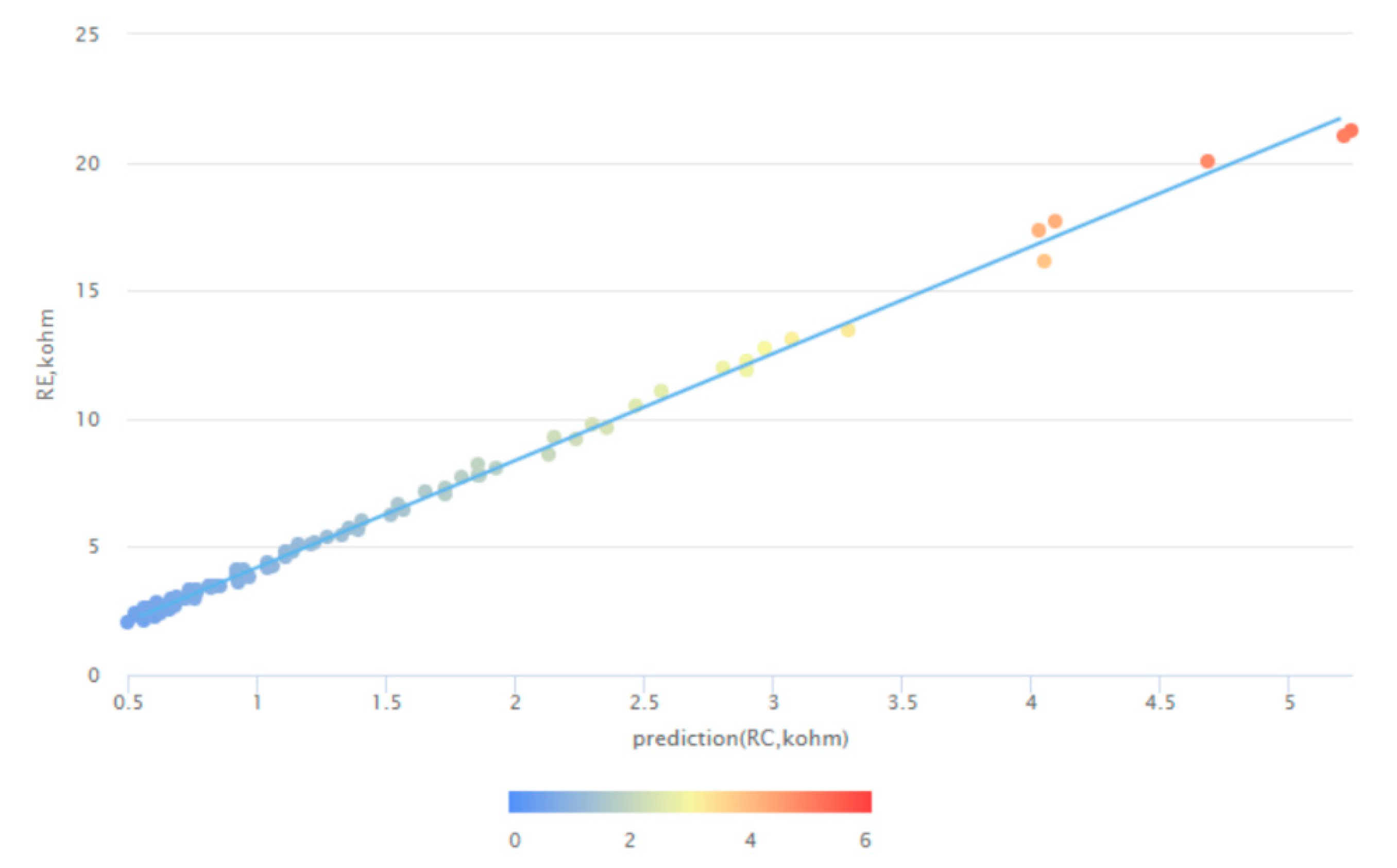
5. Results
| If , then it is an Output stage; If , then it is an Input stage; else it is an Intermediate stage. |
| If , then it is an Input stage; If and , then it is an Output stage; If and , then it is an Intermediate stage. |
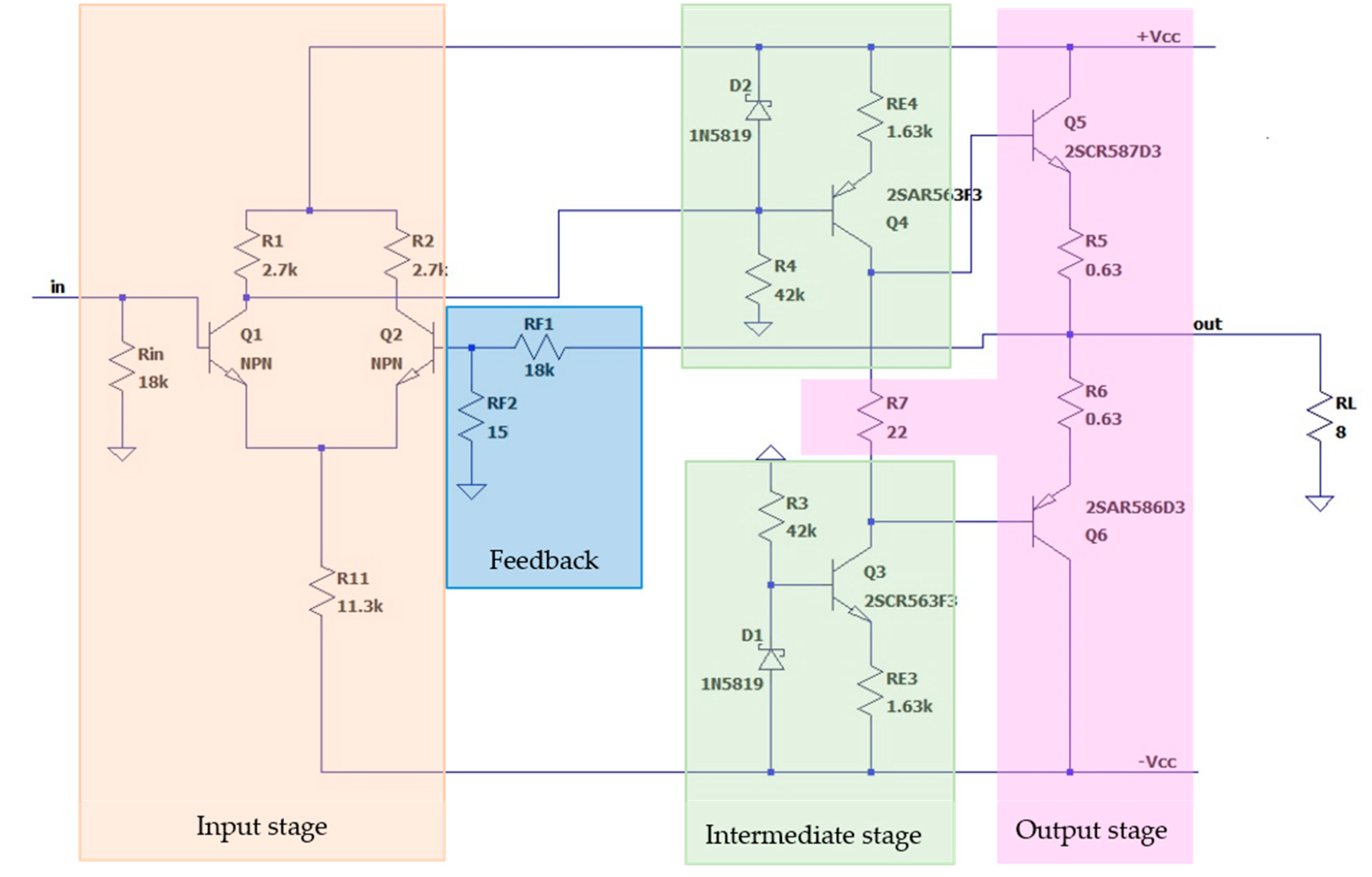
6. Case Study
7. Conclusions
Author Contributions
Funding
Conflicts of Interest
References
- Franco, S. Analog Circuit Design: Discrete & Integrated, 1st ed.; McGraw Hill: New York, NY, USA, 2014. [Google Scholar]
- Gray, P.R.; Hurst, P.J.; Lewis, S.H.; Meyer, R.G. Analysis and Design of Analog Integrated Circuits, 5th ed.; Wiley: Hoboken, NJ, USA, 2009. [Google Scholar]
- Fallon, E. Machine Learning in EDA: Opportunities and Challenges. In Proceedings of the 2020 ACM/IEEE 2nd Workshop on Machine Learning for CAD (MLCAD), Reykjavik, Iceland, 16–20 November 2020; p. 103. [Google Scholar]
- Gubbi, K.I.; Beheshti-Shirazi, S.A.; Sheaves, T.; Salehi, S.; Manoj, S.; Rafatirad, S.; Sasan, A.; Homayoun, H. Survey of Machine Learning for Electronic Design Automation. In Proceedings of the Great Lakes Symposium on VLSI 2022, Irvine, CA, USA, 6–8 June 2022. [Google Scholar]
- Pandey, M. Machine Learning and Systems for Building the Next Generation of EDA Tools. In Proceedings of the 2018 23rd Asia and South Pacific Design Automation Conference (ASP-DAC), Jeju, Korea, 22–25 January 2018; pp. 411–415. [Google Scholar]
- Dahiya, N.; Gupta, S.; Singh, S. A Review Paper on Machine Learning Applications, Advantages, and Techniques. ECS Trans. 2022, 107, 6137–6150. [Google Scholar] [CrossRef]
- Dash, S.S.; Nayak, S.K.; Mishra, D. A Review on Machine Learning Algorithms. In Intelligent and Cloud Computing. Smart Innovation, Systems and Technologies; Mishra, D., Buyya, R., Mohapatra, P., Patnaik, S., Eds.; Springer: Singapore, 2021. [Google Scholar]
- Dineva, K.; Atanasova, T. Systematic Look at Machine Learning Algorithms—Advantages, Disadvantages and Practical Applications. In Proceedings of the 20th International Multidisciplinary Scientific GeoConference SGEM 2020, Albena, Bulgaria, 18–24 August 2020; pp. 317–324. [Google Scholar]
- Hamolia, V.; Melnyk, V. A Survey of Machine Learning Methods and Applications in Electronic Design Automation. In Proceedings of the 2021 11th International Conference on Advanced Computer Information Technologies (ACIT), Deggendorf, Germany, 15–17 September 2021; pp. 757–760. [Google Scholar]
- Ren, H.; Khailany, B.; Fojtik, M.; Zhang, Y. Machine Learning and Algorithms: Let Us Team Up for EDA. IEEE Des. Test 2022. [Google Scholar] [CrossRef]
- Dieste-Velasco, M.I.; Diez-Mediavilla, M.; Alonso-Tristán, C. Regression and ANN Models for Electronic Circuit Design. Complexity 2018, 2018, 7379512. [Google Scholar] [CrossRef]
- Guerra-Gomez, I.; McConaghy, T.; Tlelo-Cuautle, E. Study of Regression Methodologies on Analog Circuit Design. In Proceedings of the 2015 16th Latin-American Test Symposium (LATS), Puerto Vallarta, Mexico, 25–27 March 2015; pp. 1–6. [Google Scholar]
- Hasani, R.M.; Haerle, D.; Baumgartner, C.F.; Lomuscio, A.R.; Grosu, R. Compositional neural-network modeling of complex analog circuits. In Proceedings of the 2017 International Joint Conference on Neural Networks (IJCNN), Anchorage, AL, USA, 14–19 May 2017; pp. 2235–2242. [Google Scholar]
- Mina, R.; Jabbour, C.; Sakr, G.E. A Review of Machine Learning Techniques in Analog Integrated Circuit Design Automation. Electronics 2022, 11, 435. [Google Scholar] [CrossRef]
- Markov, I.L.; Hu, J.; Kim, M. Progress and Challenges in VLSI Placement Research. Proc. IEEE 2015, 103, 1985–2003. [Google Scholar] [CrossRef]
- Yan, J.; Lyu, X.; Cheng, R.; Lin, Y. Towards Machine Learning for Placement and Routing in Chip Design: A Methodological Overview. arXiv 2022, arXiv:2202.13564. [Google Scholar]
- Barboza, E.C.; Shukla, N.; Chen, Y.; Hu, J. Machine Learning-Based Pre-Routing Timing Prediction with Reduced Pessimism. In Proceedings of the 56th Annual Design Automation Conference, New York, NY, USA, 2–6 June 2019. [Google Scholar]
- Nariman, N.A.; Hamdia, K.; Ramadan, A.M.; Sadaghian, H. Optimum Design of Flexural Strength and Stiffness for Reinforced Concrete Beams Using Machine Learning. Appl. Sci. 2021, 11, 8762. [Google Scholar] [CrossRef]
- Hensel, S.; Marinov, M.B.; Schmitt, M. Object Detection and Mapping with Unmanned Aerial Vehicles Using Convolutional Neural Networks. In Future Access Enablers for Ubiquitous and Intelligent Infrastructures; Perakovic, D., Knapcikova, L., Eds.; Springer: Cham, Switzerland, 2021; Volume 382, pp. 254–267. [Google Scholar]
- Huang, C.Y.; Lin, I.C.; Liu, Y.L. Applying Deep Learning to Construct a Defect Detection System for Ceramic Substrates. Appl. Sci. 2022, 12, 2269. [Google Scholar] [CrossRef]
- De la Rosa, F.L.; Sánchez-Reolid, R.; Gómez-Sirvent, J.L.; Morales, R.; Fernández-Caballero, A. A Review on Machine and Deep Learning for Semiconductor Defect Classification in Scanning Electron Microscope Images. Appl. Sci. 2021, 11, 9508. [Google Scholar] [CrossRef]
- Grout, I. Digital Systems Design with FPGAs and CPLDs; Elsevier: Amsterdam, The Netherlands, 2008. [Google Scholar]
- Issakov, V. CMOS and Bipolar Technologies. In Microwave Circuits for 24 GHz Automotive Radar in Silicon-based Technologies; Springer: Berlin, Germany, 2010. [Google Scholar]
- Vida-Torku, E.K.; Reohr, W.; Monzel, J.A.; Nigh, P. Bipolar, CMOS and BiCMOS Circuit Technologies Examined for Testability. In Proceedings of the 34th Midwest Symposium on Circuits and Systems, Monterey, CA, USA, 14–17 May 1991; pp. 1015–1020. [Google Scholar]
- Trade-offs Between CMOS, JFET, and Bipolar Input Stage Technology. Available online: https://www.ti.com/lit/an/sboa355/sboa355.pdf?ts=1660033873955&ref_url=https%253A%252F%252Fwww.bing.com%252F (accessed on 26 July 2022).
- Huang, G.; Hu, J.; He, Y.; Liu, J.; Ma, M.; Shen, Z.; Wu, J.; Xu, Y.; Zhang, H.; Zhong, K.; et al. Machine Learning for Electronic Design Automation: A Survey. ACM Trans. Des. Autom. Electron. Syst. 2021, 26, 1–46. [Google Scholar] [CrossRef]
- Ren, H. Embracing Machine Learning in EDA. In Proceedings of the 2022 International Symposium on Physical Design (ISPD’22), Singapore, 27–30 March 2022; pp. 55–56. [Google Scholar]
- Donevska, L.; Stamenov, D.; Pandiev, I.M.; Asparuhova, K.; Yakimov, P.I. Tutorial for Seminar Practices on Analog Electronics; Technical Univesity of Sofia: Sofia, Bulgaria, 2008. [Google Scholar]
- Nenov, G. Analog Electronics; Novi Znania: Sofia, Bulgaria, 2006. [Google Scholar]
- Pandiev, I. Analog Electronics; Technical Univesity of Sofia: Sofia, Bulgaria, 2015. [Google Scholar]
- Ivanova, M. Analog Electronics; Technical Univesity of Sofia: Sofia, Bulgaria, 2020. [Google Scholar]
- 2SCR587D3 NPN 3A 120V Power Transistor. Available online: https://fscdn.rohm.com/en/products/databook/datasheet/discrete/transistor/bipolar/2scr587d3tl1-e.pdf (accessed on 26 July 2022).
- 2SAR586D3 PNP -5.0A -80V Power Transistor. Available online: https://fscdn.rohm.com/en/products/databook/datasheet/discrete/transistor/bipolar/2sar586d3tl1-e.pdf (accessed on 26 July 2022).
- 2SCR563F3 NPN 6A 50V Middle Power Transistor. Available online: https://fscdn.rohm.com/en/products/databook/datasheet/discrete/transistor/bipolar/2scr563f3tr-e.pdf (accessed on 26 July 2022).
- 2SAR563F3 PNP -6A -50V Middle Power Transistor. Available online: https://fscdn.rohm.com/en/products/databook/datasheet/discrete/transistor/bipolar/2sar563f3tr-e.pdf (accessed on 26 July 2022).
- 2N3904 NPN General—Purpose Amplifier. Available online: https://www.onsemi.com/pdf/datasheet/2n3904-d.pdf (accessed on 26 July 2022).
- Axial Lead Rectifiers. Available online: https://www.onsemi.com/pdf/datasheet/1n5817-d.pdf (accessed on 26 July 2022).
- Rapid Miner Studio Platform. Available online: https://rapidminer.com/ (accessed on 26 July 2022).
- Grzymala-Busse, J.W. Rule Induction. In Data Mining and Knowledge Discovery Handbook; Maimon, O., Rokach, L., Eds.; Springer: Boston, MA, USA, 2009. [Google Scholar]
- Pham, D.T.; Bigot, S.; Dimov, S.S. RULES-5: A rule induction algorithm for classification problems involving continuous attributes. Proc. Inst. Mech. Eng. C J. Mech. Eng. Sci. 2003, 217, 1273–1286. [Google Scholar] [CrossRef] [Green Version]
- Raczko, E.; Zagajewski, B. Comparison of support vector machine, random forest and neural network classifiers for tree species classification on airborne hyperspectral APEX images. Eur. J. Remote Sens. 2013, 50, 144–154. [Google Scholar] [CrossRef]
- Adugna, T.; Xu, W.; Fan, J. Comparison of Random Forest and Support Vector Machine Classifiers for Regional Land Cover Mapping Using Coarse Resolution FY-3C Images. Remote Sens. 2022, 14, 574. [Google Scholar] [CrossRef]


| Stage | Parameters | Function | Type |
|---|---|---|---|
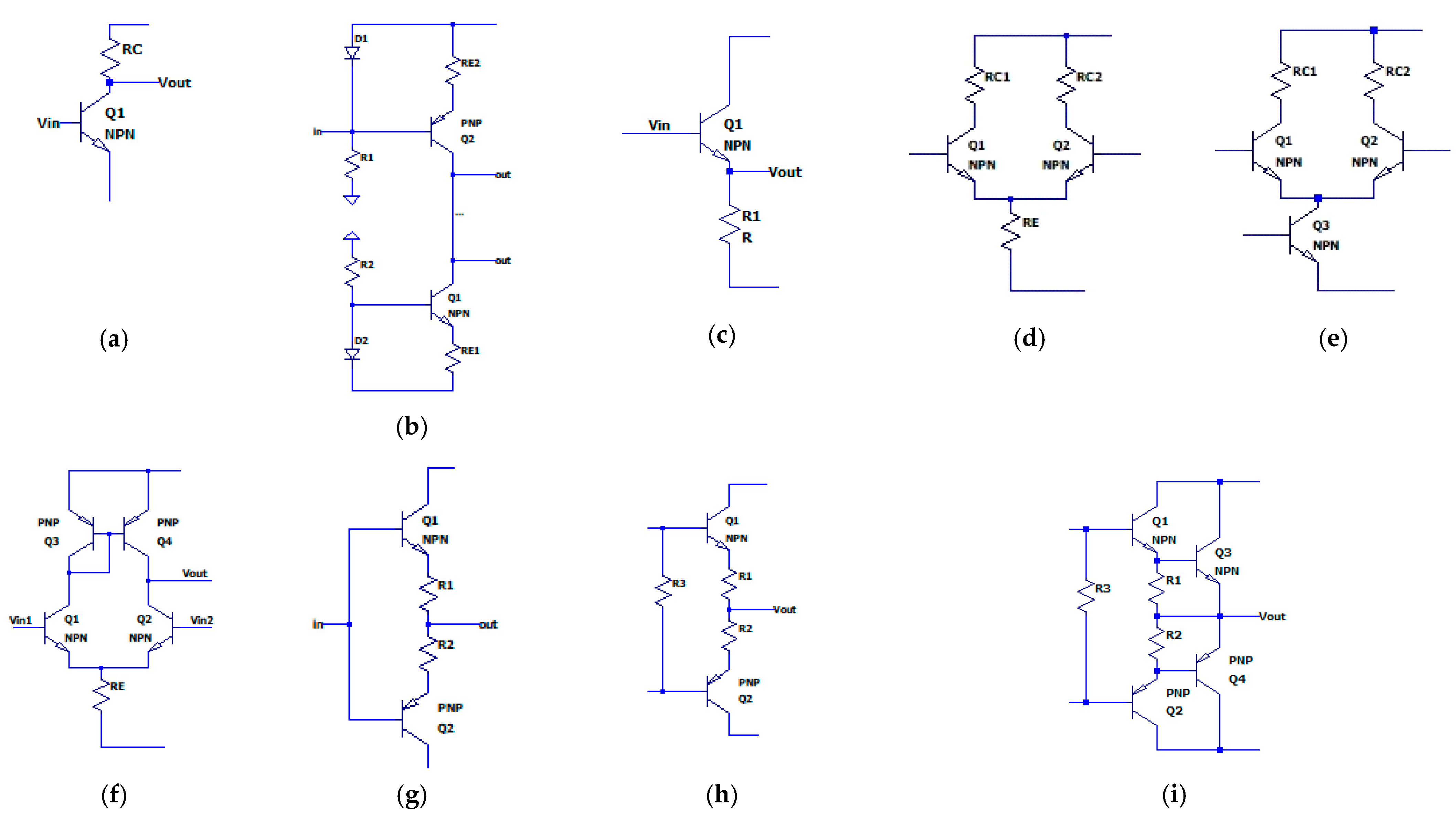
| (a) Stage 1: common emitter | —medium | Amplifies voltage, current, and power, inverts the phase of the input voltage by 180° | Intermediate |
| (b) Stage 2: common emitter with active load | —high | Amplifies voltage, current, and power, possesses increased amplification gains | Intermediate |
| (c) Stage 3: common collector | —low | Repeats the input voltage (voltage follower), but amplifies the current and power | Output |
| (d) Stage 4: differential pair with resistive load and emitter resistor | —high | Amplifies the difference between both inputs | Input |
| (e) Stage 5: differential pair with resistive load and current source; | —higher | Better suppression of common mode signals | Input |
| (f) Stage 6: differential pair with active load | —higher | Higher differential gain is achieved through adding active load | Input |
| (g) Stage 7: push-pull stage with complementary output pair in class B | Each of the transistors operates in an CC circuit, which achieves high input and low output resistance, high current gain and low distortion. | Output | |
| (h) Stage 8: complementary output pair in class AB | The resistor R3 is used for creating a bias voltage on the bases of transistors T1 and T2 | Output | |
| (i) Stage 9: complementary output pair with Darlington transistors in class AB | The two diodes, in addition to creating a bias voltage on the bases of transistors T1 and T2, are also used to stabilize their operating current | Output |
| CMRR | Circuit | Stage Type | |||||
|---|---|---|---|---|---|---|---|
| high | n/a | high | medium | high | n/a | diff. pair with resistive load | input |
| higher | n/a | high | medium | high | n/a | diff. pair with active load | input |
| high | n/a | high | medium | higher | n/a | diff. pair with current source | input |
| high | high | medium | medium | n/a | n/a | common emitter | intermediate |
| higher | high | medium | high | n/a | n/a | common emitter with active load | intermediate |
| does not amplify | high | high | Low | n/a | medium | push-pull class AB | output |
| … | … | … | … | … | … | … | … |
| 1.2 | 1.2 | 1.58 | 0.75 | 0.75 | 24 |
| 1.1 | 1.1 | 1.58 | 0.69 | 0.69 | 23 |
| 1 | 1 | 1.58 | 0.63 | 0.63 | 22 |
| … | … | … | … | … | … |
| 14.7 | 14.7 | 1.63 | 1.63 | 42 | 42 |
| 15.19 | 15.19 | 1.57 | 1.57 | 42 | 42 |
| 15.68 | 15.68 | 1.53 | 1.53 | 42 | 42 |
| … | … | … | … | … | … |
| 22.6 | 0.5 | 5.4 | 19.23 | 67.432 | 12 | 10.8 |
| 18.833 | 0.6 | 4.5 | 23.076 | 71.618 | 13 | 9 |
| 16.142 | 0.7 | 3.857 | 26.923 | 74.941 | 14 | 7.714 |
| 14.125 | 0.8 | 3.375 | 30.769 | 77.641 | 15 | 6.75 |
| 12.555 | 0.9 | 3 | 34.615 | 79.881 | 16 | 6 |
| 11.3 | 1 | 2.7 | 38.461 | 81.768 | 18 | 5.4 |
| … | … | … | … | … | … | … |
Publisher’s Note: MDPI stays neutral with regard to jurisdictional claims in published maps and institutional affiliations. |
© 2022 by the authors. Licensee MDPI, Basel, Switzerland. This article is an open access article distributed under the terms and conditions of the Creative Commons Attribution (CC BY) license (https://creativecommons.org/licenses/by/4.0/).
Share and Cite
Ivanova, M.; Stošović, M.A. Machine Learning and Rules Induction in Support of Analog Amplifier Design. Computation 2022, 10, 145. https://doi.org/10.3390/computation10090145
Ivanova M, Stošović MA. Machine Learning and Rules Induction in Support of Analog Amplifier Design. Computation. 2022; 10(9):145. https://doi.org/10.3390/computation10090145
Chicago/Turabian StyleIvanova, Malinka, and Miona Andrejević Stošović. 2022. "Machine Learning and Rules Induction in Support of Analog Amplifier Design" Computation 10, no. 9: 145. https://doi.org/10.3390/computation10090145