
From Traditional to Novel Printed Electrochromic Devices: Material, Structure and Device

 , , and
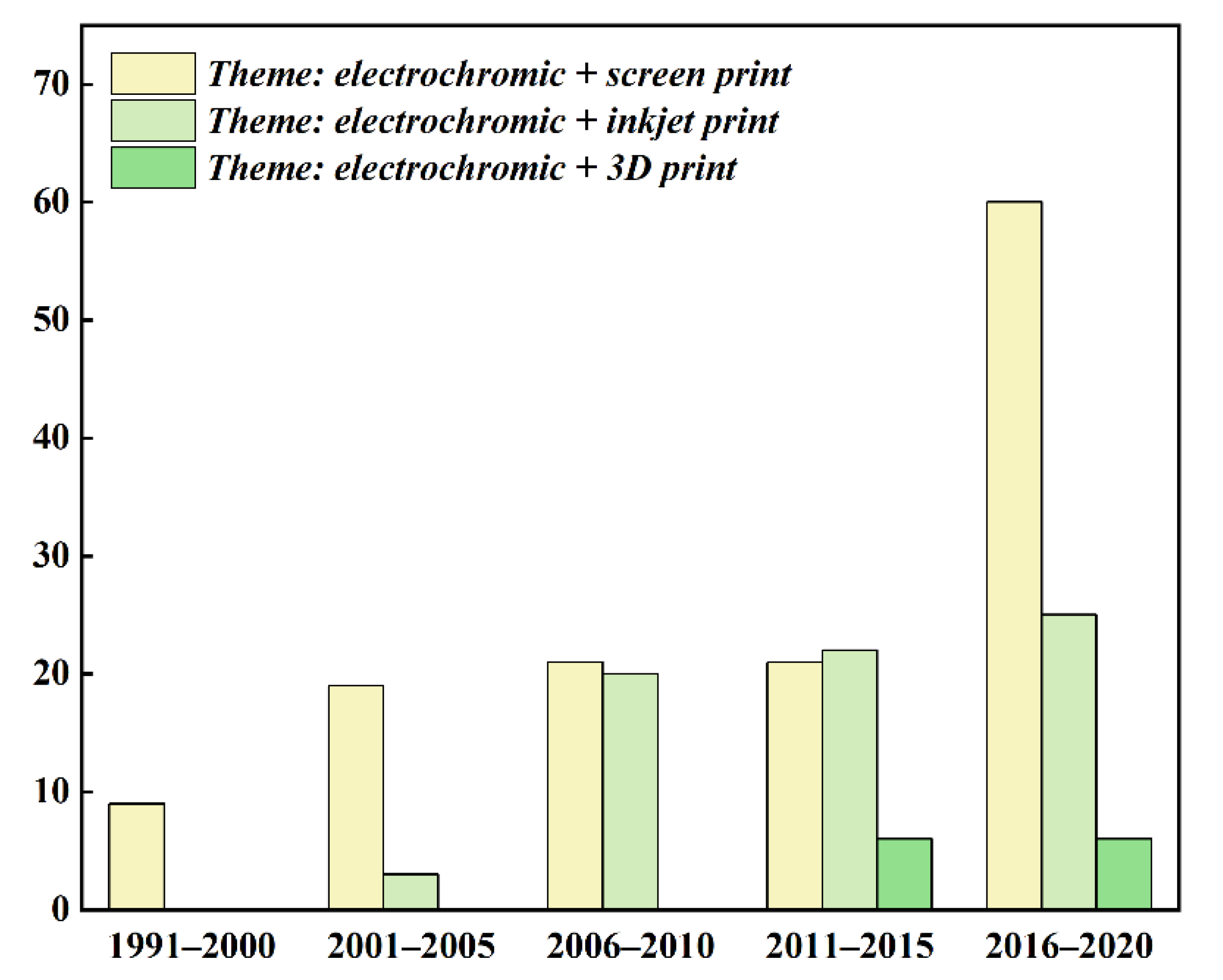
Abstract
:1. Introduction
2. Printed Electrochromic Device
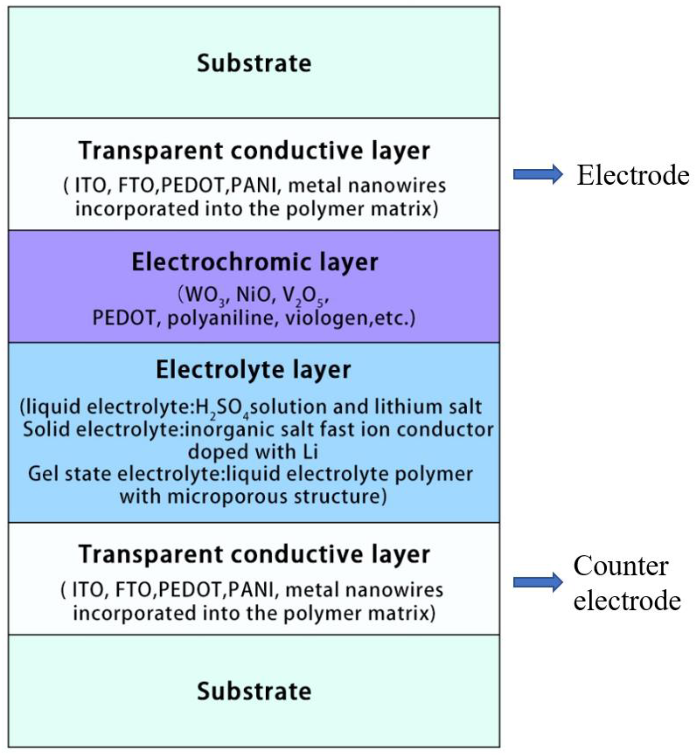
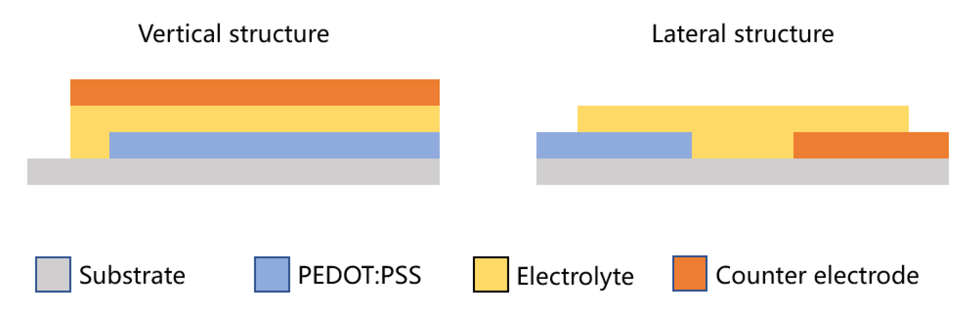
2.1. A Typical Structure of Electrochromic Device
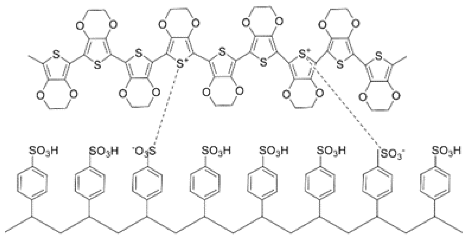
2.2. Printed Electrochromic Materials
2.3. Screen Printing Electrochromic Devices
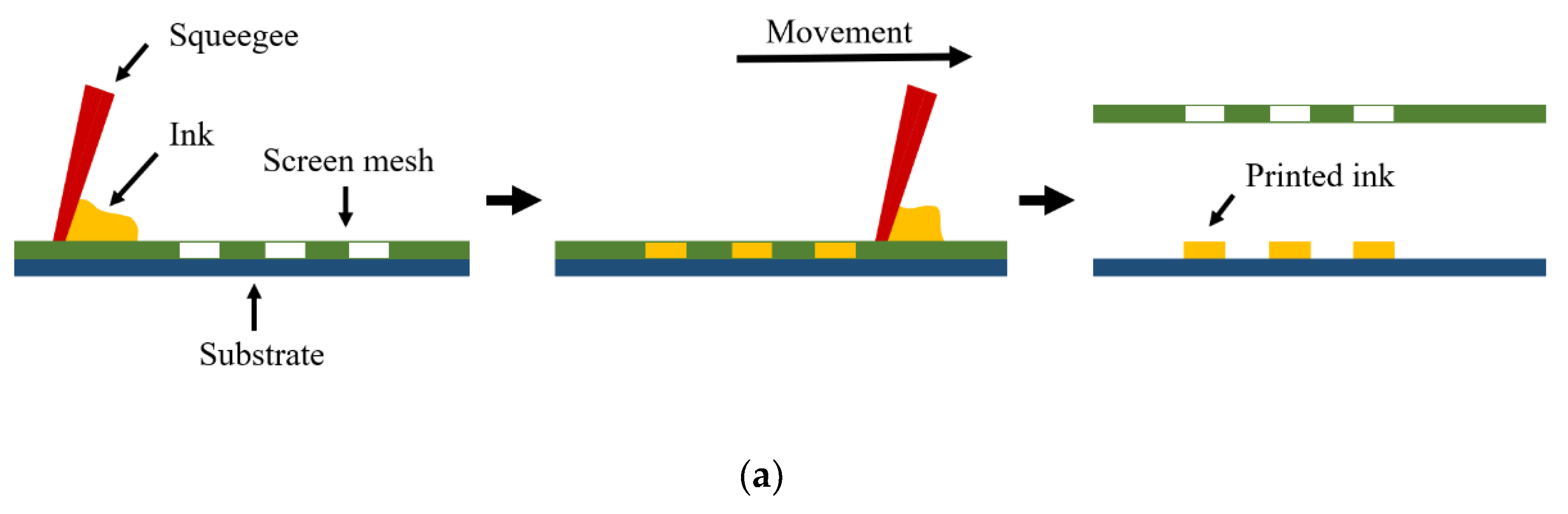
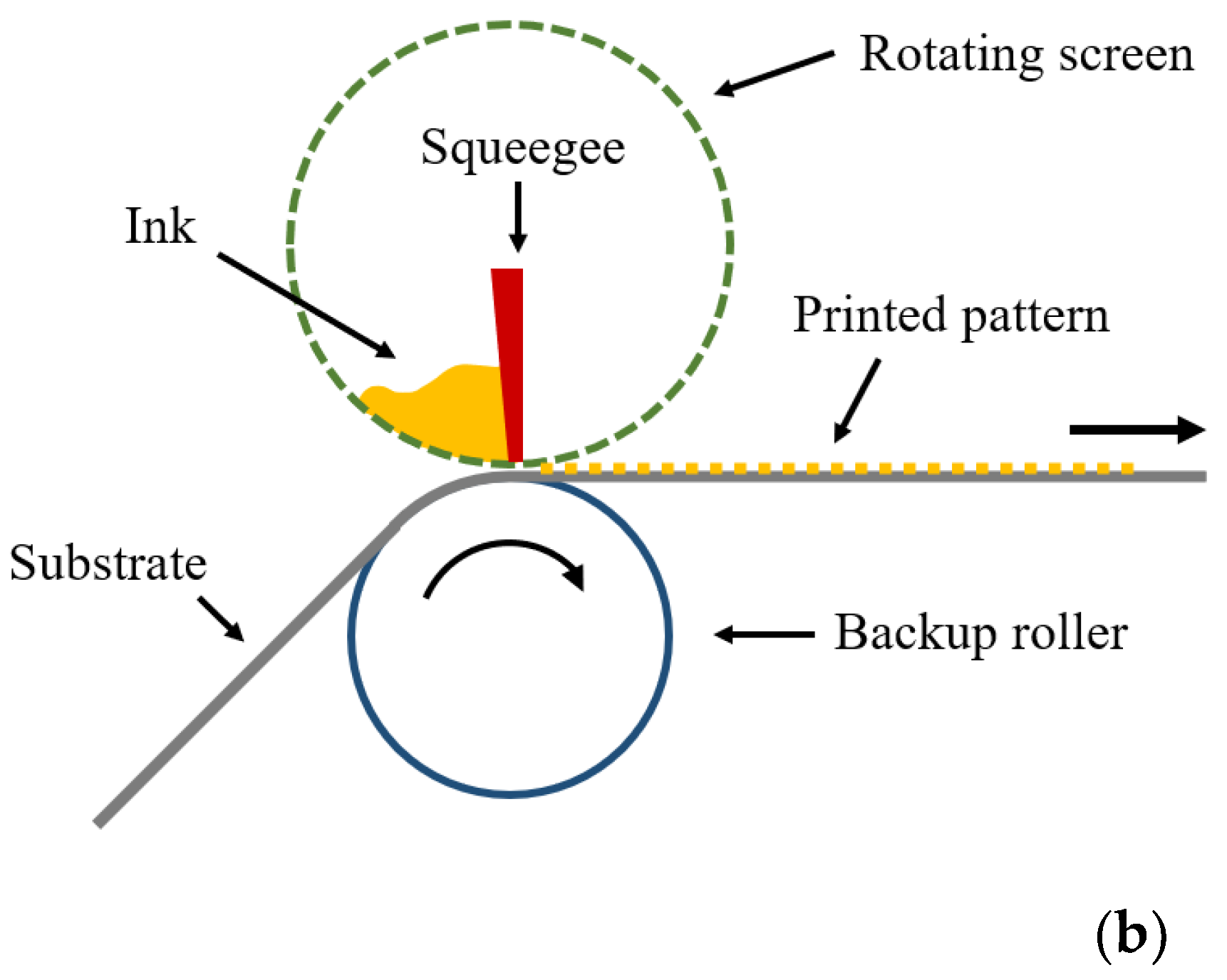
2.3.1. General Idea of the Screen Printing Process
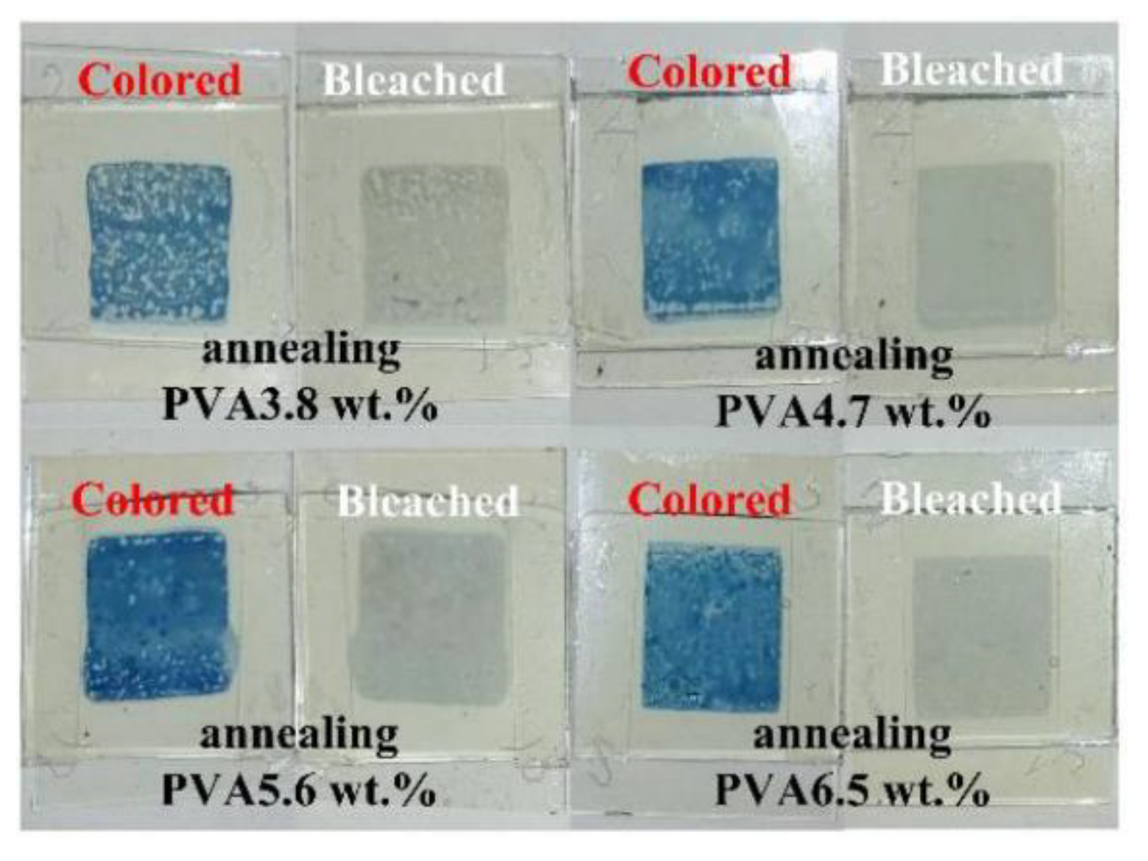
2.3.2. Research on the Application of Screen Printing on Electrochromic Devices
- 1.
- Electrode
- 2.
- Electrochromic layer
- 3.
- Electrolyte layer
- 4.
- Screen-printed Electrochromic Displays
2.4. Inkjet Printing Electrochromic Devices
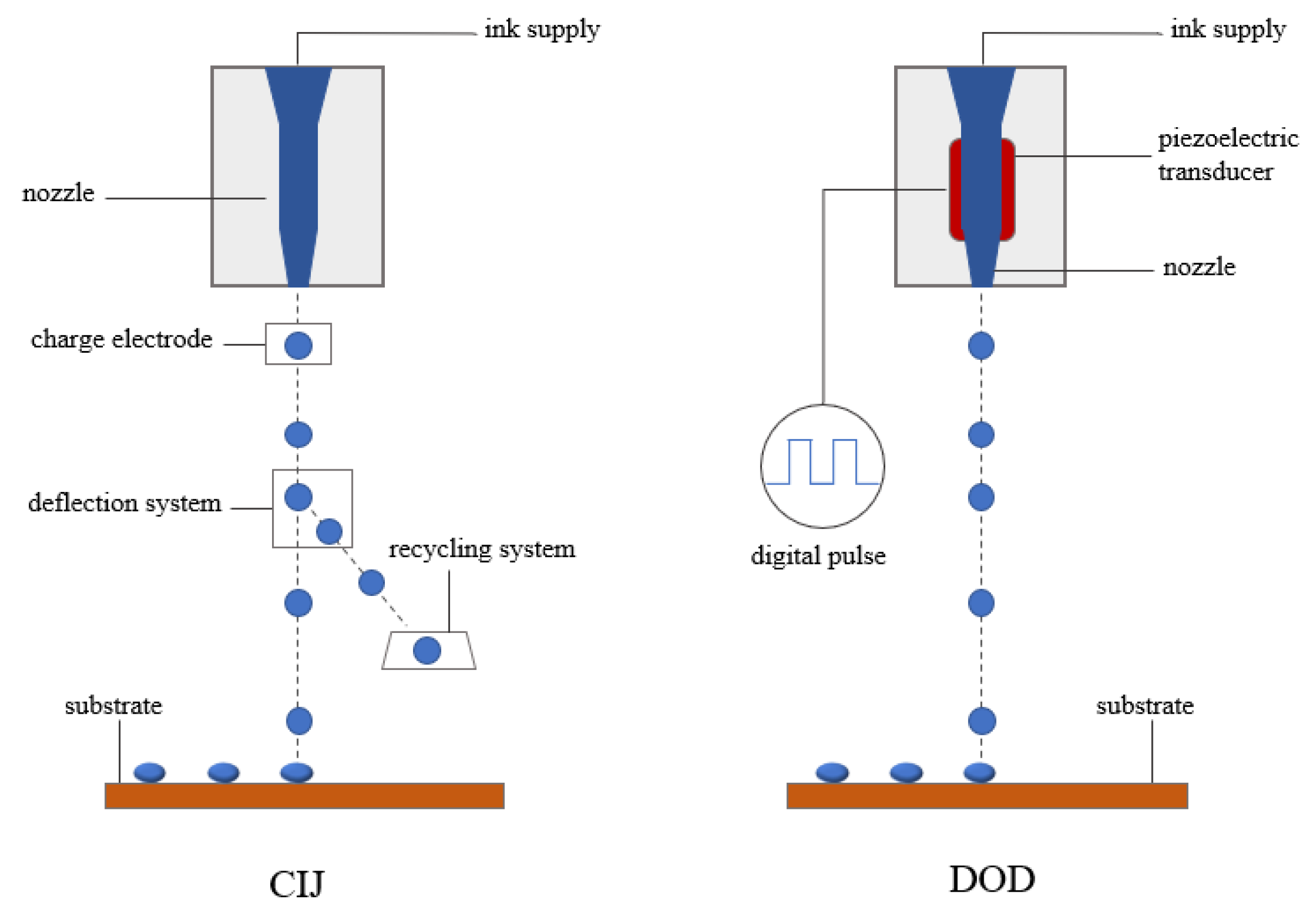
2.4.1. General Idea of the Inkjet Printing Process
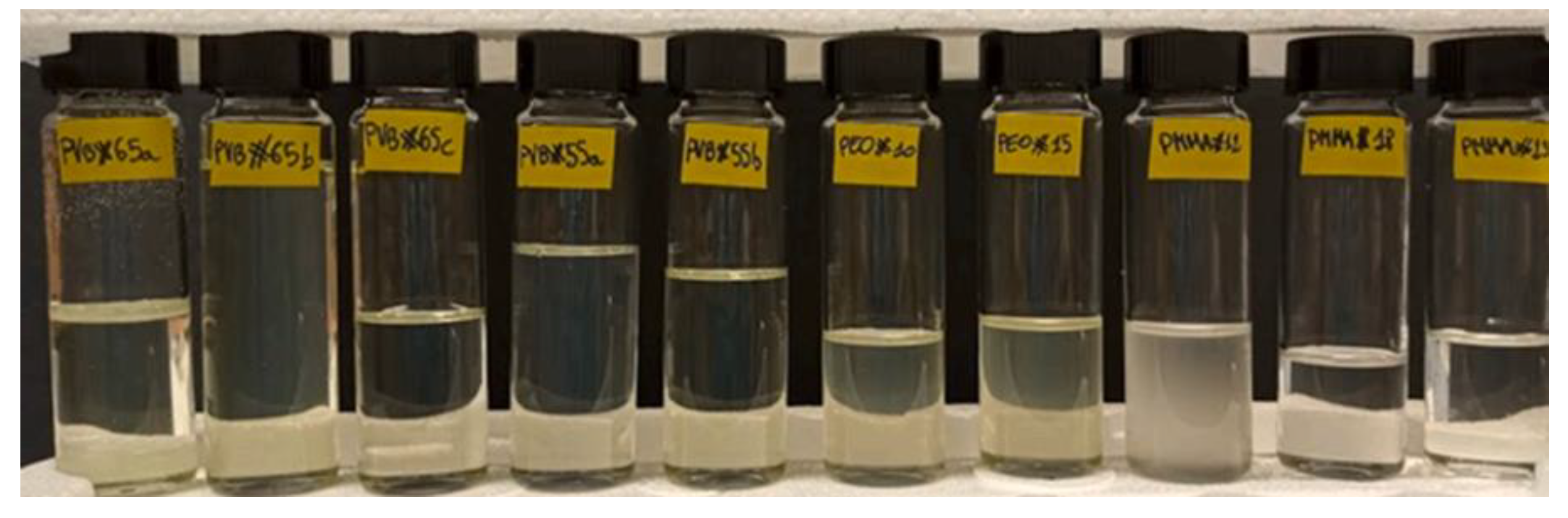
2.4.2. Research on the Application of Inkjet Printing on Electrochromic Devices
- Electrode
- 2.
- Electrochromic layer
- 3.
- Electrolyte layer
2.5. 3D Printing Electrochromic Devices
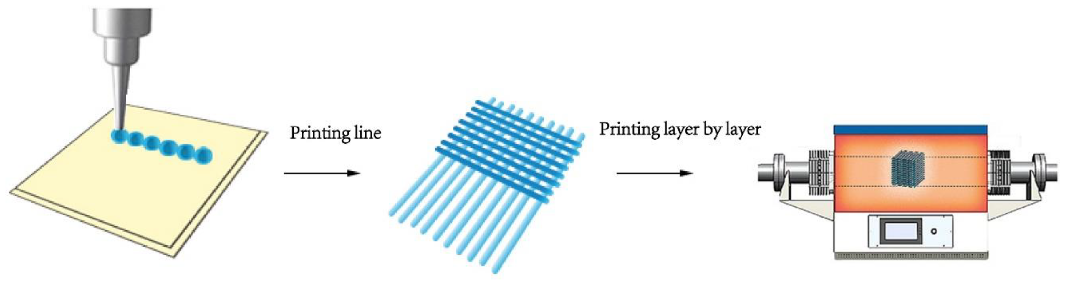
2.5.1. General Idea of the 3D Printing Process
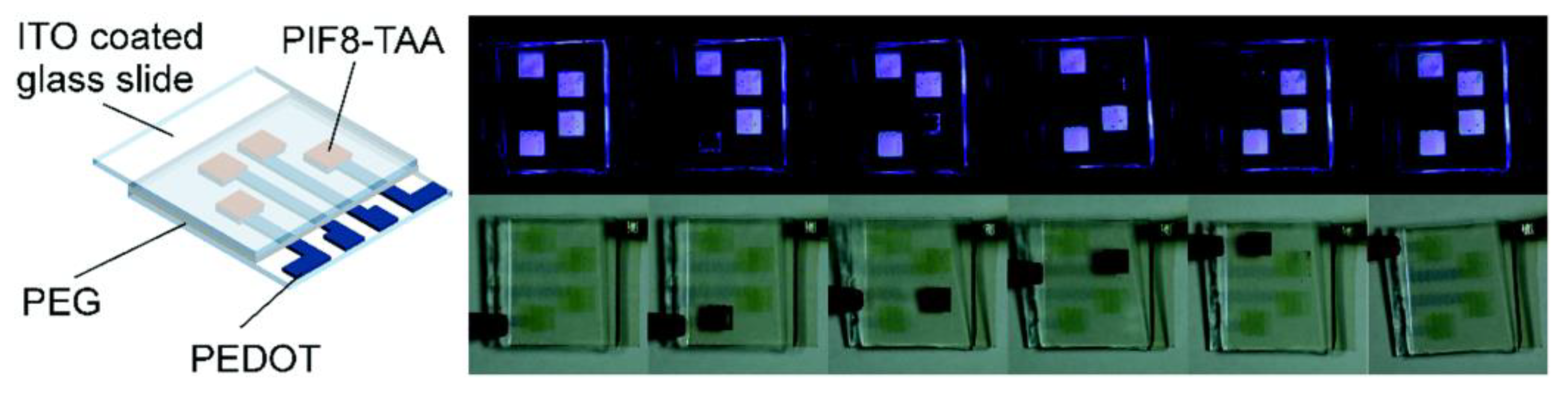
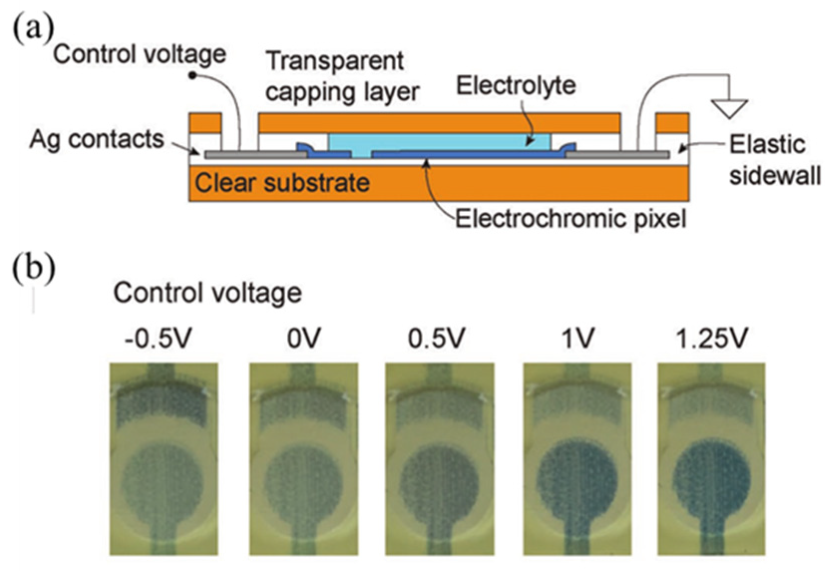
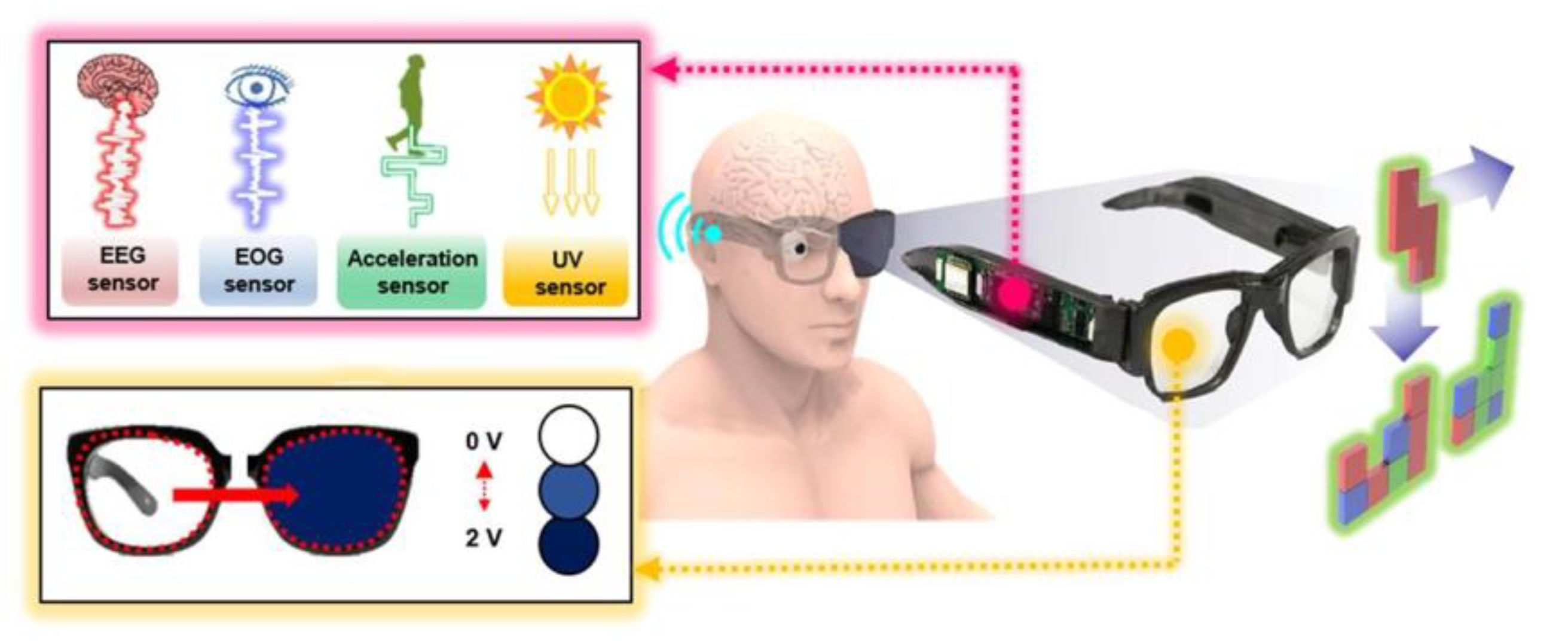
2.5.2. Research on the Application of 3D Printing on Electrochromic Devices
- Electrode
- 2.
- Electrochromic layer
- 3.
- Electrolyte layer
3. Summary
Author Contributions
Funding
Institutional Review Board Statement
Informed Consent Statement
Data Availability Statement
Conflicts of Interest
References
- Huang, Z.; Song, J.; Pan, L.; Zhang, X.; Wang, L.; Zhou, J. Tungsten Oxides for Photocatalysis, Electrochemistry, and Phototherapy. Adv. Mater. 2015, 27, 5309–5327. [Google Scholar] [CrossRef] [PubMed]
- Cong, S.; Tian, Y.; Li, Q.; Zhao, Z.; Geng, F. Single-Crystalline Tungsten Oxide Quantum Dots for Fast Pseudocapacitor and Electrochromic Applications. Adv. Mater. 2014, 26, 4260–4267. [Google Scholar] [CrossRef] [PubMed]
- Liu, J.; Zhang, G.; Guo, K.; Guo, D.; Shi, M.; Ning, H.; Qiu, T.; Chen, J.; Fu, X.; Yao, R. Effect of the Ammonium Tungsten Precursor Solution with the Modification of Glycerol on Wide Band Gap WO3 Thin Film and Its Electrochromic Properties. Micromachines 2020, 11, 311. [Google Scholar] [CrossRef] [PubMed] [Green Version]
- Zheng, H.; Qu, J.; Strano, M.S.; Kaner, R.B.; Mitchell, A.; Kalantar-Zadeh, K. Nanostructured Tungsten Oxide—Properties, Synthesis, and Applications. Adv. Funct. Mater. 2011, 21, 2175–2196. [Google Scholar] [CrossRef]
- Zhang, G.; Lu, K.; Zhang, X.; Yuan, X.; Ning, H.; Tao, R.; Liu, X.; Yao, R.; Peng, J. Enhanced Transmittance Modulation of SiO2-Doped Crystalline WO3 Films Prepared from a Polyethylene Oxide (PEO) Template. Coatings 2018, 8, 228. [Google Scholar] [CrossRef] [Green Version]
- Santato, C.; Odziemkowski, M.; Ulmann, M.; Augustynski, J. Crystallographically oriented Mesoporous WO3 films: Synthesis, characterization, and applications. J. Am. Chem. Soc. 2001, 123, 10639–10649. [Google Scholar] [CrossRef]
- Niklasson, G.A.; Granqvist, C.G. Electrochromics for smart windows: Thin films of tungsten oxide and nickel oxide, and devices based on these. J. Mater. Chem. 2007, 17, 127–156. [Google Scholar] [CrossRef] [Green Version]
- Granqvist, C.G.; Azens, A.; Smulko, J.; Kish, L. Oxide-based electrochromics for energy efficient buildings: Materials, technologies, testing, and perspectives. J. Phys. Conf. Ser. 2007, 93, 012021. [Google Scholar]
- Baetens, R.; Jelle, B.P.; Gustavsen, A. Properties, requirements and possibilities of smart windows for dynamic daylight and solar energy control in buildings: A state-of-the-art review. Sol. Energy Mater. Sol. Cells. 2010, 94, 87–105. [Google Scholar] [CrossRef] [Green Version]
- Cheng, W.; He, J.; Dettelbach, K.; Johnson, N.; Sherbo, R.; Berlinguette, C. Photodeposited Amorphous Oxide Films for Electrochromic Windows. Chem 2018, 4, 821–832. [Google Scholar] [CrossRef] [Green Version]
- Cai, G.; Eh, A.; Ji, L.; Lee, P. Recent Advances in Electrochromic Smart Fenestration. Adv. Sustain. Syst. 2017, 1, 1700074. [Google Scholar] [CrossRef]
- Lampert, C.M. Electrochromic materials and devices for energy efficient windows. Sol. Energy Mater. 1984, 11, 1–27. [Google Scholar] [CrossRef] [Green Version]
- Chen, Y.; Xu, Z.; Sun, J.L.; Deng, H.T.; Chen, H.T.; Zhao, Y.L. Industrial status and future of large area intelligent electrochromic glass. J. Funct. Mater. 2013, 44, 2441–2446. (In Chinese) [Google Scholar]
- Jaksic, N.I.; Salahifar, C. A feasibility study of electrochromic windows in vehicles. Sol. Energy Mater. Sol. Cells 2003, 79, 409–423. [Google Scholar] [CrossRef]
- Sottile, G.M. 2004 Survey of United States architects on the subject of switchable glazings. Mater. Sci. Eng. B Adv. Funct. Solid-State Mater. 2005, 119, 240–245. [Google Scholar] [CrossRef]
- Klems, J.H. Net energy performance measurements on electrochromic skylights. Energy Build. 2001, 33, 93–102. [Google Scholar] [CrossRef]
- Cai, G.; Wang, J.; Lee, P. Next-Generation Multifunctional Electrochromic Devices. Acc. Chem. Res. 2016, 49, 1469–1476. [Google Scholar] [CrossRef]
- Wu, N. Vehicle e.g., Car Has Electrochromic Glass That Is Electrically Connected with Electric Control Module, and Receives Control Voltage, and Changes Transparency According to Control Voltage. CN Patent CN216184378-U, 2 May 2022. [Google Scholar]
- Yoo, I.H.; Lee, S.; La, Y.; Ahn, B.; Nayongsang; Yu., I.; Liu, R.; Li, C.; Luo, L. Electrochromic Device Used as Window of Building or Car, Smart Window, or Smart Mirror, Comprises Light Transmission Variable Structure Interposed between Base Layer, Where Light Transmission Variable Structure Comprises Chromic Layers, and Electrolyte Layer Interposed between Chromic Layers. U.S. Patent US2022066275-A1, 3 March 2022. [Google Scholar]
- Zhang, H.; Li, W.; Zhao, J. Preparing Tungsten Oxide Electrochromic Film Used in Intelligent Window, Display, Anti-Glare Rearview Mirror and Air-craft Porthole, Comprises Ultrasonically Cleaning Transparent Conductive Substrate with Acetone, Ethanol and Ultra-Pure Water, Drying, and Performing Magnetron Sputtering Technique. CN Patent CN113943928-A, 18 January 2022. [Google Scholar]
- Kao, S.; Lu, H.; Kung, C.; Chen, H.; Chang, T.; Ho, K. Thermally Cured Dual Functional Viologen-Based All-in-One Electrochromic Devices with Panchromatic Modulation. ACS Appl. Mater. Interfaces 2016, 8, 4175–4184. [Google Scholar] [CrossRef]
- Knott, E.P.; Craig, M.; Liu, D.; Babiarz, J.; Dyer, A.; Reynolds, J. A minimally coloured dioxypyrrole polymer as a counter electrode material in polymeric electrochromic window devices. J. Mater. Chem. 2012, 22, 4953–4962. [Google Scholar] [CrossRef]
- Beduk, T.; Bihar, E.; Surya, S.; Castillo, A.; Inal, S.; Salama, K. A paper-based inkjet-printed PEDOT:PSS/ZnO sol-gel hydrazine sensor. Sens. Actuator B Chem. 2020, 306, 127539. [Google Scholar] [CrossRef]
- Zhang, H.; Moon, S.K.; Ngo, T.H. 3D Printed Electronics of Non-contact Ink Writing Techniques: Status and Promise. Int. J. Precis. Eng. Manuf.-Green Technol. 2020, 7, 511–524. [Google Scholar] [CrossRef]
- Du, D.X. Study on preparation and properties of printed silver nanoconductive ink. Ph.D. Thesis, University of Electronic Science and Technology of China, Chengdu, China, 2020. (In Chinese). [Google Scholar]
- Aller-Pellitero, M.; Santiago-Malagon, S.; Ruiz, J.; Alonso, Y.; Lakard, B.; Hihn, J.; Guirado, G.; del Campo, F. Fully-printed and silicon free self-powered electrochromic biosensors: Towards naked eye quantification. Sens. Actuator B Chem. 2020, 306, 127535. [Google Scholar] [CrossRef]
- Laschuk, N.O.; Ebralidze, I.; Easton, E.; Zenkina, O. Osmium- and Cobalt-Terpyridine-Based Electrochromic Devices for “Smart” Signage Application: The Effect of Lighting on Color Perception. Adv. Electron. Mater. 2021, 7, 2100460. [Google Scholar] [CrossRef]
- Maksimenko, I.; Kilian, D.; Mehringer, C.; Voigt, M.; Peukert, W.; Wellmann, P. Application of Printable ITO/PEDOT nanocomposites as transparent electrodes in optoelectronic devices. In Proceedings of the 2012 Conference on Lasers and Electro-Optics (CLEO), San Jose, CA, USA, 6–11 May 2012. [Google Scholar]
- Laschuk, N.O.; Ahmad, R.; Ebralidze, I.; Poisson, J.; Easton, E.; Zenkina, O. Multichromic Monolayer Terpyridine-Based Electrochromic Materials. ACS Appl. Mater. Interfaces 2020, 12, 41749–41757. [Google Scholar] [CrossRef] [PubMed]
- Wang, H.; Gu, W.; Liu, X.; Zhang, Q.; Li, Y.; Hou, C.; Lin, G. Preparing low-energy-consumption screen printing molybdenum-doped tungsten oxide nano-structure electrochromic film, comprises e.g., dissolving tungstic acid in hydrogen peroxide, heating, then adding molybdenum oxide, and refluxing. CN Patent CN111646706-A, 1 September 2020. [Google Scholar]
- Cai, G.; Cheng, X.; Layani, M.; Tan, A.; Li, S.; Eh, A.; Gao, D.; Magdassi, S.; Lee, P. Direct inkjet-patterning of energy efficient flexible electrochromics. Nano Energy 2018, 49, 147–154. [Google Scholar] [CrossRef]
- Huang, X.; Chen, J.; Xie, H.; Zhao, F.; Fan, S.; Zhang, Y. Inkjet printing of 2D polyaniline for fabricating flexible and patterned electrochromic devices. Sci. China-Mater. 2022, 65, 2217–2226. [Google Scholar] [CrossRef]
- Morrin, A.; Ngamna, O.; O’Malley, E.; Kent, N.; Moulton, S.; Wallace, G.; Smyth, M.; Killard, A. The fabrication and characterization of inkjet-printed polyaniline nanoparticle films. Electrochim. Acta 2008, 53, 5092–5099. [Google Scholar] [CrossRef]
- Chiolerio, A.; Sangermano, M. In situ synthesis of Ag-acrylic nanocomposites: Tomography-based percolation model, irreversible photoinduced electromigration and reversible electromigration. Mater. Sci. Eng. B Adv. Funct. Solid-State Mater. 2012, 177, 373–380. [Google Scholar] [CrossRef]
- Azhar, E.A.; Yu, H.; Alford, T. Self-Powered, Inkjet Printed Electrochromic Films On Flexible and Stretchable Substrate for Wearable Electronics Applications. In Proceedings of the 68th IEEE Electronic Components and Technology Conference (ECTC), San Diego, CA, USA, 29 May–1 June 2018. [Google Scholar]
- Cai, G.; Darmawan, P.; Cui, M.; Chen, J.; Wang, X.; Eh, A.; Magdassi, S.; Lee, P. Inkjet-printed all solid-state electrochromic devices based on NiO/WO3 nanoparticle complementary electrodes. Nanoscale 2016, 8, 348–357. [Google Scholar] [CrossRef]
- Chang-Jian, C.; Cho, E.; Yen, S.; Lee, K.; Huang, J.; Hsiao, Y. Facile preparation of WO3/PEDOT:PSS composite for inkjet printed electrochromic window and its performance for heat shielding. Dye. Pigments 2018, 148, 465–473. [Google Scholar] [CrossRef]
- Pietsch, M.; Schlisske, S.; Held, M.; Strobel, N.; Wieczorek, A.; Hernandez-Sosa, G. Biodegradable inkjet-printed electrochromic display for sustainable short-lifecycle electronics. J. Mater. Chem. C. 2020, 8, 16716–16724. [Google Scholar] [CrossRef]
- Costa, C.; Pinheiro, C.; Henriques, I.; Laia, C. Electrochromic Properties of Inkjet Printed Vanadium Oxide Gel on Flexible Polyethylene Terephthalate/Indium Tin Oxide Electrodes. ACS Appl. Mater. Interfaces. 2012, 4, 5266–5275. [Google Scholar] [CrossRef] [PubMed]
- Yekefallah, V.; Soleimani-Gorgani, A.; Rouhani, S.; Najafi, F. Ink-jet Printing for the Fabrication of a Flexible Electrochromic Device Based on the Water-Soluble Viologen-Functionalized Dendrimer. J. Electrochem. Sci. Technol. 2021, 12, 146–158. [Google Scholar] [CrossRef]
- Xu Kaixuan. Fabrication and Research of Colorful Flexible Electrochromic Devices. Ph.D. Thesis, Donghua University, Shanghai, China, 2019. (In Chinese).
- Han, W.M.; Zheng, Q.; Wang., L.; Yan, D. Research progress of printed electronic technology. In 2017 Electronic Glass Technology Paper Compilation; Sun Sdn. Bhd: Beijing, China, 2017. (In Chinese) [Google Scholar]
- He, W.; Yang, Y.; He, B.; Hu, K. Preparation technology and application of conductive ink. Mater. Rev. 2009, 23, 30–33. (In Chinese) [Google Scholar]
- Li, L.H.; Mo, L.; Ran, J.; Xin, Z. Conductive ink and its application. Image Sci. Photochemistry 2014, 32, 393–401. [Google Scholar]
- Pande, G.K.; Kim, N.; Choi, J.H.; Balamurugan, G.; Moon, H.C.; Park, J.S. Effects of counter ions on electrochromic behaviors of asymmetrically substituted viologens. Sol. Energy Mater. Sol. Cells 2019, 197, 25–31. [Google Scholar] [CrossRef]
- Frolov, D.G.; Petrov, M.M.; Makhaeva, E.E.; Keshtov, M.L.; Khokhlov, A.R. Electrochromic behavior of poly(pyridinium triflates) films: Electrolyte ions influence. Synth. Metals 2018, 239, 29–35. [Google Scholar] [CrossRef]
- Yadav, P.; Naqvi, S.; Patra, A. Poly(3,4-ethylenedioxyselenophene): Effect of solvent and electrolyte on electrodeposition, optoelectronic and electrochromic properties. Rsc. Adv. 2020, 10, 12395–12406. [Google Scholar] [CrossRef] [PubMed]
- Danine, A.; Manceriu, L.; Faure, C.; Labrugere, C.; Penin, N.; Delattre, A.; Eymin-Petot-Tourtollet, G.; Rougier, A. Toward Simplified Electrochromic Devices Using Silver as Counter Electrode Material. ACS Appl. Mater. Interfaces 2019, 11, 34030–34038. [Google Scholar] [CrossRef]
- Zhou, Y.; Wang, J. Electrochromic device used for e.g., smart window and display technology comprises electrochromic film that comprises first electrochromic layer having reduction colored material, solid state electrolyte, and second electrochromic layer having oxidation colored material. USA US2021347686-A1, 11 November 2021. [Google Scholar]
- Zanarini, S.; Garino, N.; Nair, J.; Francia, C.; Wojcik, P.; Pereira, L.; Fortunato, E.; Martins, R.; Bodoardo, S.; Penazzi, N. Contrast Enhancement in Polymeric Electrochromic Devices Encompassing Room Temperature Ionic Liquids. Int. J. Electrochem. Sci. 2014, 9, 1650–1662. [Google Scholar]
- Theodosiou, K.; Giannopoulos, P.; Georgakopoulos, T.; Stathatos, E. Quasi-Solid-State Electrochromic Cells with Energy Storage Properties Made with Inkjet Printing. Materials 2020, 13, 3241. [Google Scholar] [CrossRef]
- Thakur, V.K.; Ding, G.; Ma, J.; Lee, P.; Lu, X. Hybrid Materials and Polymer Electrolytes for Electrochromic Device Applications. Adv. Mater. 2012, 24, 4071–4096. [Google Scholar] [CrossRef] [PubMed]
- Granqvist, C.G.; Arvizu, M.; Pehlivan, I.; Qu, H.; Wen, R.; Niklasson, G. Electrochromic materials and devices for energy efficiency and human comfort in buildings: A critical review. Electrochim. Acta 2018, 259, 1170–1182. [Google Scholar] [CrossRef] [Green Version]
- Yuan, G. Preparation, Structure and Properties of Electrochromic Tungsten Oxide Nanocrystalline Composite Films. Ph.D. Thesis, Zhejiang University, Hangzhou, China, 2018. (In Chinese). [Google Scholar]
- Linderhed, U.; Petsagkourakis, I.; Ersman, P.; Beni, V.; Tybrandt, K. Fully screen printed stretchable electrochromic displays. Flex. Print. Electron. 2021, 6, 045014. [Google Scholar] [CrossRef]
- Krebs, F.C. Fabrication and processing of polymer solar cells: A review of printing and coating techniques. Sol. Energy Mater. Sol. Cells 2009, 93, 394–412. [Google Scholar] [CrossRef]
- Guo, K.; Zhang, G.; Long, Y.; Ning, H.; Xu, Z.; Qiu, T.; Luo, D.; Li, M.; Yao, R.; Peng, J. Modifying Precursor Solutions to Obtain Screen-Printable Inks for Tungsten Oxides Electrochromic Film Preparation. Coatings 2021, 11, 872. [Google Scholar] [CrossRef]
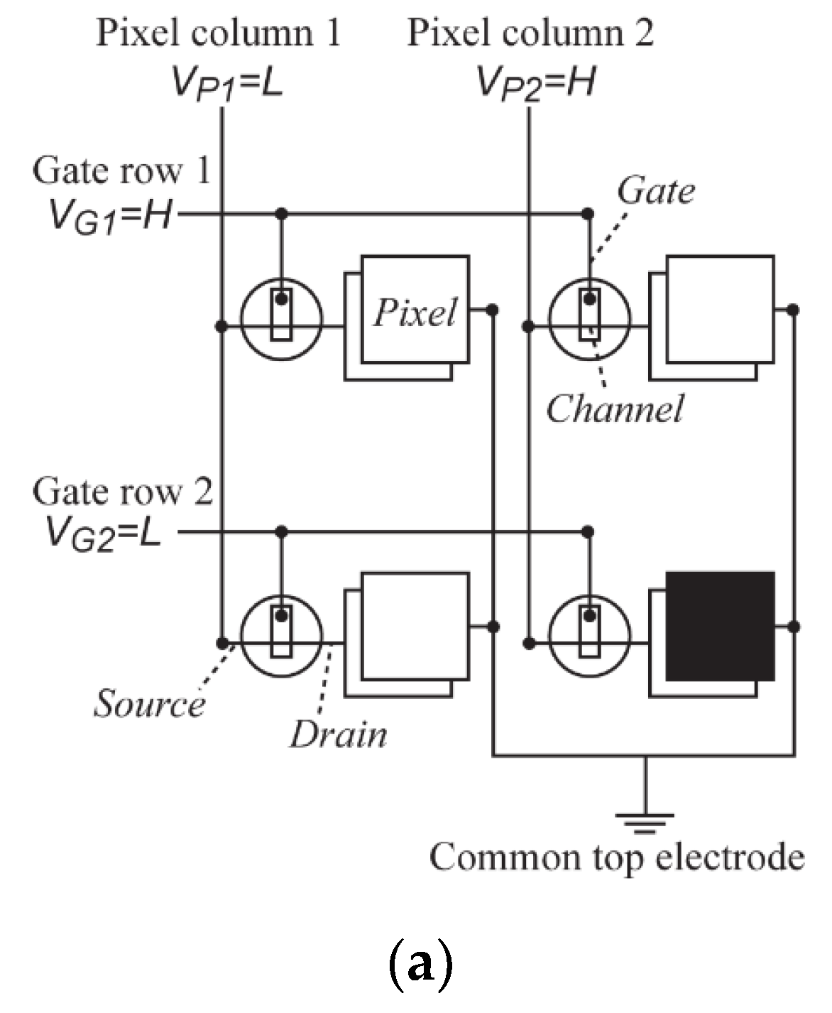
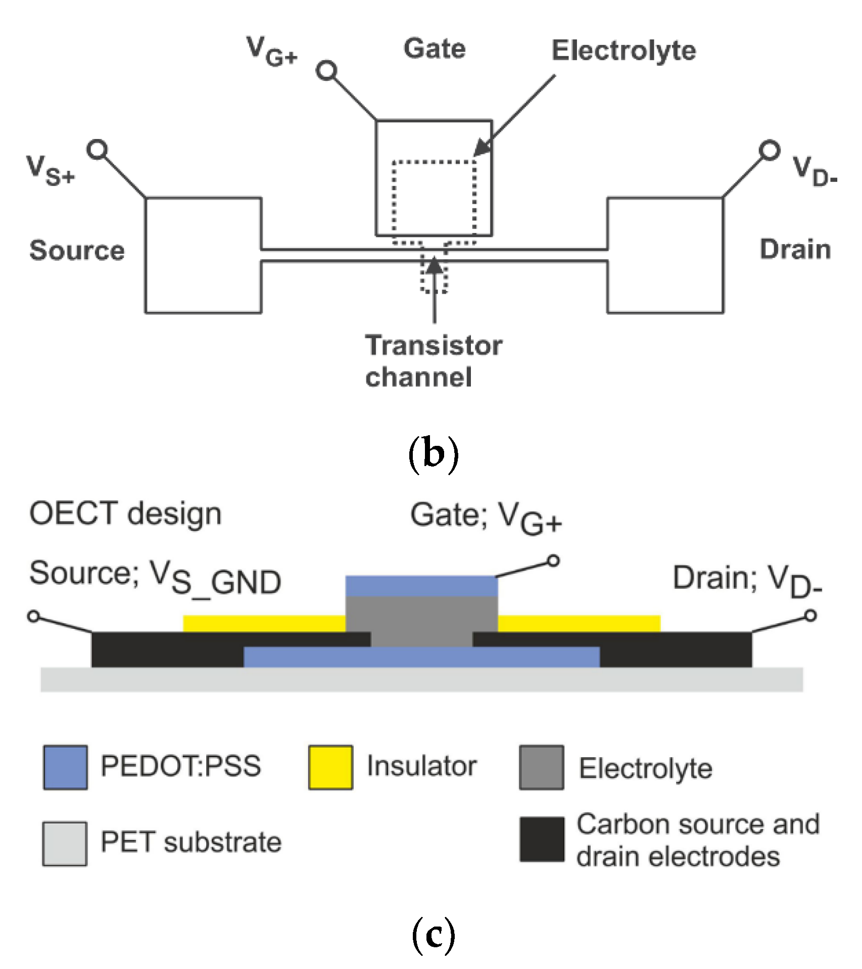
- Cao, X.; Lau, C.; Liu, Y.; Wu, F.; Gui, H.; Liu, Q.; Ma, Y.; Wan, H.; Amer, M.; Zhou, C. Fully Screen-Printed, Large-Area, and Flexible Active-Matrix Electrochromic Displays Using Carbon Nanotube Thin-Film Transistors. ACS Nano 2016, 10, 9816–9822. [Google Scholar] [CrossRef] [PubMed]
- Andersson Ersman, P.; Freitag, K.; Kawahara, J.; Ahlin, J. The rise of electrochromics through dynamic QR codes and grayscale images in screen printed passive matrix addressed displays. Sci. Rep. 2022, 12, 10959. [Google Scholar] [CrossRef]
- Andersson Ersman, P.; Kawahara, J.; Berggren, M. Printed passive matrix addressed electrochromic displays. Org. Electron. 2013, 14, 3371–3378. [Google Scholar] [CrossRef] [Green Version]
- Weng, W.; Higuchi, T.; Suzuki, M.; Fukuoka, T.; Shimomura, T.; Ono, M.; Radhakrishnan, L.; Wang, H.; Suzuki, N.; Oveisi, H. A High-Speed Passive-Matrix Electrochromic Display Using a Mesoporous TiO2 Electrode with Vertical Porosity. Angew. Chem. Int. Edit. 2010, 49, 3956–3959. [Google Scholar] [CrossRef]
- Andersson, P.; Forchheimer, R.; Tehrani, P.; Berggren, M. Printable all-organic electrochromic active-matrix displays. Adv. Funct. Mater. 2007, 17, 3074–3082. [Google Scholar] [CrossRef]
- Liu, G.; Liu, Y.; Zhang, M.; Yang, Z.; Gane, P. Comparing build architecture and electrolyte of ITO-free flexible patterned organic screen-printed ECDs based on a novel PEDOT:PSS compound film post-treated with strong and weak organic acids. Org. Electron. 2020, 81, 105674. [Google Scholar] [CrossRef]
- Andersson Ersman, P.; Lassnig, R.; Strandberg, J.; Dyreklev, P. Flexible Active Matrix Addressed Displays Manufactured by Screen Printing. Adv. Eng. Mater. 2021, 23, 2000771. [Google Scholar] [CrossRef]
- Cots, A.; Dicorato, S.; Giovannini, L.; Favoino, F.; Manca, M. Energy Efficient Smart Plasmochromic Windows: Properties, Manufacturing and Integration in Insulating Glazing. Nano Energy 2021, 84, 2000771. [Google Scholar] [CrossRef]
- Santiago, S.; Aller, M.; del Campo, F.; Guirado, G. Screen-printable Electrochromic Polymer Inks and Ion Gel Electrolytes for the Design of Low-power, Flexible Electrochromic Devices. Electroanalysis 2019, 31, 1664–1671. [Google Scholar] [CrossRef]
- Ahmad, R.; Dipalo, V.; Bell, M.; Ebralidze, I.; Zenkina, O.; Easton, E. Surface-Enhanced Counter Electrode Materials for the Fabrication of Ultradurable Electrochromic Devices. ACS Appl. Energ. Mater. 2022, 5, 3905–3914. [Google Scholar] [CrossRef]
- Fan, X.; Nie, W.; Tsai, S.; Wang, N.; Huang, H.; Cheng, Y.; Wen, R.; Ma, L.; Yan, F.; Xia, Y. PEDOT:PSS for Flexible and Stretchable Electronics: Modifications, Strategies, and Applications. Adv. Sci. 2019, 6, 1900813. [Google Scholar] [CrossRef] [Green Version]
- Aller-Pellitero, M.; Fremeau, J.; Villa, R.; Guirado, G.; Lakard, B.; Hihn, J.; del Campo, F. Electrochromic biosensors based on screen-printed Prussian Blue electrodes. Sens. Actuator B Chem. 2019, 290, 591–597. [Google Scholar] [CrossRef] [Green Version]
- Santiago-Malagón, S.; Rio-Colin, D.; Azizkhani, H.; Aller-Pellitero, M.; Guirado, G.; del Campo, F. A self-powered skin-patch electrochromic biosensor. Biosens. Bioelectron. 2021, 175, 112879. [Google Scholar] [CrossRef]
- Chaudhary, A.; Pathak, D.; Tanwar, M.; Sagdeo, P.; Kumar, R. Prussian Blue-Viologen Inorganic-Organic Hybrid Blend for Improved Electrochromic Performance. ACS Appl. Electron. Mater. 2019, 1, 892. [Google Scholar] [CrossRef]
- Coleman, J.P.; Lynch, A.; Madhukar, P.; Wagenknecht, J. Printed, flexible electrochromic displays using interdigitated electrodes. Sol. Energy Mater. Sol. Cells 1999, 56, 395–418. [Google Scholar] [CrossRef]
- Kawahara, J.; Ersman, P.; Nilsson, D.; Katoh, K.; Nakata, Y.; Sandberg, M.; Nilsson, M.; Gustafsson, G.; Berggren, M. Flexible active matrix addressed displays manufactured by printing and coating techniques. J. Polym. Sci. Pt. B Polym Phys. 2013, 51, 265–271. [Google Scholar] [CrossRef] [Green Version]
- Lan, L.; Zou, J.; Jiang, C.; Liu, B.; Wang, L.; Peng, J. Inkjet printing for electroluminescent devices: Emissive materials, film formation, and display prototypes. Front. Optoelectron. 2017, 10, 329–352. [Google Scholar] [CrossRef]
- Zhang, G.; Zhang, J.; Qiu, T.; Ning, H.; Fang, Z.; Zhong, J.; Yao, R.; Luo, D.; Peng, J. Fabrication of flexible electrochromic film based on amorphous isopolytungstate by low-temperature inkjet-printed process with a solution crystallization kinetic-controlled strategy. Chem. Eng. J. 2022, 427, 131840. [Google Scholar] [CrossRef]
- Gao, M.; Li, L.; Song, Y. Inkjet printing wearable electronic devices. J. Mater. Chem. C 2017, 5, 2971–2993. [Google Scholar] [CrossRef]
- Cummins, G.; Desmulliez, M.P.Y. Inkjet printing of conductive materials: A review. Circuit World 2012, 38, 193–213. [Google Scholar] [CrossRef]
- Lan, M. Preparation of High Resolution Polymer Light-Emitting Diode Display Screen by Wet Method and Related Research. Ph.D. Thesis, South China University of Technology, Guangzhou, China, 2018. (In Chinese). [Google Scholar]
- Song, W. Study on Water-Based Dye Inks for Color Inkjet Printer. Ph.D. Thesis, Xi’an University of Technology, Xi’an, China, 2005. (In Chinese). [Google Scholar]
- Small, W.R.; Masdarolomoor, F.; Wallace, G.; Panhuis, M. Inkjet deposition and characterization of transparent conducting electroactive polyaniline composite films with a high carbon nanotube loading fraction. J. Mater. Chem. 2007, 17, 4359–4361. [Google Scholar] [CrossRef]
- Kinner, L.; Nau, S.; Popovic, K.; Sax, S.; Burgues-Ceballos, I.; Hermerschmidt, F.; Lange, A.; Boeffel, C.; Choulis, S.; List-Kratochvil, E. Inkjet-printed embedded Ag-PEDOT:PSS electrodes with improved light out coupling effects for highly efficient ITO-free blue polymer light emitting diodes. Appl. Phys. Lett. 2017, 110, 101107. [Google Scholar] [CrossRef] [Green Version]
- Santos, L.; Wojcil, P.; Pinto, J.; Elangovan, E.; Viegas, J.; Pereira, L.; Martins, R.; Fortunato, E. Structure and Morphologic Influence of WO3 Nanoparticles on the Electrochromic Performance of Dual-Phase a-WO3/WO3 Inkjet Printed Films. Adv. Electron. Mater. 2015, 1, 1–2. [Google Scholar]
- Costa, C.; Pinheiro, C.; Henriques, I.; Laia, C. Inkjet Printing of Sol–Gel Synthesized Hydrated Tungsten Oxide Nanoparticles for Flexible Electrochromic Devices. ACS Appl. Mater. Interfaces 2012, 4, 1330–1340. [Google Scholar] [CrossRef]
- Wojcik, P.J.; Pereira, L.; Martins, R.; Fortunato, E. Statistical Mixture Design and Multivariate Analysis of Inkjet Printed a-WO3/TiO2/WOX Electrochromic Films. ACS Comb. Sci. 2014, 16, 5–16. [Google Scholar] [CrossRef]
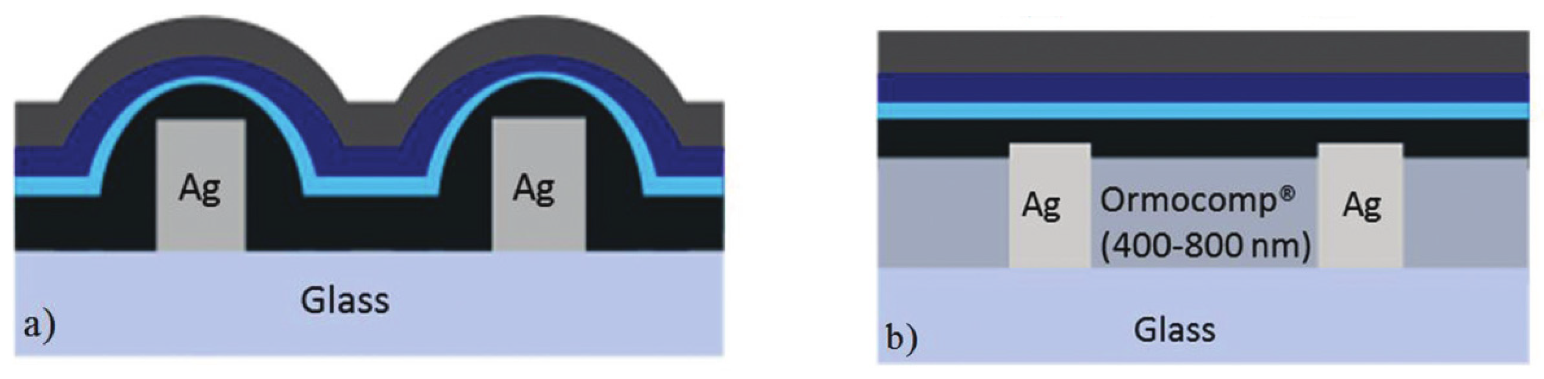
- Layani, M.; Darmawan, P.; Foo, W.; Liu, L.; Kamyshny, A.; Mandler, D.; Magdassi, S.; Lee, P. Nanostructured electrochromic films by inkjet printing on large area and flexible transparent silver electrodes. Nanoscale 2014, 6, 4572–4576. [Google Scholar] [CrossRef]
- Möller, M.; Asaftei, S.; Corr, D.; Ryan, M.; Walder, L. Switchable Electrochromic Images Based on a Combined Top–Down Bottom–Up Approach. Adv. Mater. 2004, 16, 1558–1562. [Google Scholar] [CrossRef]
- Han, F.S.; Higuchi, M.; Kurth, D.G. Metallosupramolecular polyelectrolytes self-assembled from various pyridine ring-substituted bisterpyridines and metal ions: Photophysical, electrochemical, and electrochromic properties. J. Am. Chem. Soc. 2008, 130, 2073–2081. [Google Scholar] [CrossRef]
- Higuchi, M. Electrochromic Organic-Metallic Hybrid Polymers: Fundamentals and Device Applications. Polym. J. 2009, 41, 511–520. [Google Scholar] [CrossRef] [Green Version]
- Chen, B.; Kao, S.; Hu, C.; Higuchi, M.; Ho, K.; Liao, Y. Printed Multicolor High-Contrast Electrochromic Devices. ACS Appl. Mater. Interfaces 2015, 7, 25069–25076. [Google Scholar] [CrossRef]
- Pietsch, M.; Rodlmeier, T.; Schlisske, S.; Zimmermann, J.; Romero-Nieto, C.; Hernandez-Sosa, G. Inkjet-printed polymer-based electrochromic and electrofluorochromic dual-mode displays. J. Mater. Chem. C 2019, 7, 7121–7127. [Google Scholar] [CrossRef] [Green Version]
- Pietsch, M.; Schlisske, S.; Held, M.; Maag, P.; Hernandez-Sosa, G. Stretchable inkjet-printed electronics on mechanically compliant island-bridge architectures covalently bonded to elastomeric substrates. Flex. Print. Electron. 2022, 7, 025007. [Google Scholar] [CrossRef]
- Marques, A.C.L.; Baptista, C.A.P.; Araujo, J.; Lopes Marques, A.C.; Pinheiro Baptista, C.A. Electrolyte Solution for Electrochromic Cell for Printing Techniques, such as Inkjet Printing, Comprises Ionic Compound, Monomer, Oligomer or Polymer, Photoinitiator and Polar Solvent, Where Ionic Compound Is Lithium Perchlorate. POR. WO2013095170-A1, 27 June 2013. [Google Scholar]
- Kondo, Y.; Tanabe, H.; Kudo, H.; Nakano, K.; Otake, T. Electrochromic Type E-Paper Using Poly(1H-Thieno [3,4-d]Imidazol-2(3H)-One) Derivatives by a Novel Printing Fabrication Process. Materials 2011, 4, 2171–2182. [Google Scholar] [CrossRef] [Green Version]
- Chang, P.; Mei, H.; Zhang, M.; Zhao, Y.; Wang, X.; Cheng, L.; Zhang, L. 3D Printed Electrochromic Supercapacitors with Ultrahigh Mechanical Strength and Energy Density. Small 2021, 17, 2102639. [Google Scholar] [CrossRef]
- Sundaram, S.; Jiang, Z.; Sitthi-Amorn, P.; Kim, D.S.; Baldo, M.A.; Matusik, W. 3D-Printed Autonomous Sensory Composites. Adv. Mater. Technol. 2017, 2, 1600257. [Google Scholar] [CrossRef]
- Lee, J.H.; Kim, H.; Huang, J.; Chung, J.; Jang, T.; Seo, D.; Gao, Y.; Lee, J.; Park, H.; Lee, S. 3D Printed, Customizable, and Multifunctional Smart Electronic Eyeglasses for Wearable Healthcare Systems and Human-Machine Interfaces. ACS Appl. Mater. Interfaces 2020, 12, 21424–21432. [Google Scholar] [CrossRef] [PubMed]
- Ha, M.; Zhang, W.; Braga, D.; Renn, M.; Kim, C.; Frisbie, C. Aerosol-Jet-Printed, 1 Volt H-Bridge Drive Circuit on Plastic with Integrated Electrochromic Pixel. ACS Appl. Mater. Interfaces 2013, 5, 13198–13206. [Google Scholar] [CrossRef] [PubMed]
- Sundaram, S.; Kim, D.; Baldo, M.; Hayward, R.; Matusikt, W. 3D-Printed Self-Folding Electronics. ACS Appl. Mater. Interfaces 2017, 9, 32290–32298. [Google Scholar] [CrossRef] [PubMed]


Publisher’s Note: MDPI stays neutral with regard to jurisdictional claims in published maps and institutional affiliations. |
© 2022 by the authors. Licensee MDPI, Basel, Switzerland. This article is an open access article distributed under the terms and conditions of the Creative Commons Attribution (CC BY) license (https://creativecommons.org/licenses/by/4.0/).
Share and Cite
Cai, Q.; Yan, H.; Yao, R.; Luo, D.; Li, M.; Zhong, J.; Yang, Y.; Qiu, T.; Ning, H.; Peng, J. From Traditional to Novel Printed Electrochromic Devices: Material, Structure and Device. Membranes 2022, 12, 1039. https://doi.org/10.3390/membranes12111039
Cai Q, Yan H, Yao R, Luo D, Li M, Zhong J, Yang Y, Qiu T, Ning H, Peng J. From Traditional to Novel Printed Electrochromic Devices: Material, Structure and Device. Membranes. 2022; 12(11):1039. https://doi.org/10.3390/membranes12111039
Chicago/Turabian StyleCai, Qingyue, Haoyang Yan, Rihui Yao, Dongxiang Luo, Muyun Li, Jinyao Zhong, Yuexin Yang, Tian Qiu, Honglong Ning, and Junbiao Peng. 2022. "From Traditional to Novel Printed Electrochromic Devices: Material, Structure and Device" Membranes 12, no. 11: 1039. https://doi.org/10.3390/membranes12111039