1. Introduction
An efficient integrated waveguide is undoubtedly the basis of the development of photonic integrated circuits. A valuable candidate needs to have excellent characteristics such as subwavelength mode constraints, chip scale propagation length, high efficiency waveguide bending, and small center-to-center separation between low crosstalk adjacent waveguides.
Recently, reports of plasmonic waveguides such as metal-dielectric-metal (MDM) [
1], dielectric-metal-dielectric (DMD) [
2], hybrid surface plasmon polariton (HSPP) [
3,
4,
5], and dielectric loaded surface plasmon polariton (DLSPP) [
6], have generated considerable attention. Plasmonic waveguides can bound light into the deep subwavelength scale, and enhance light–matter interactions [
7,
8]. However, due to the collective oscillation of electrons at the interface between metal and medium with Ohm dissipation, the propagation loss is high. It is impossible to achieve medium or even small scale waveguide integration, and the practical prospect is severely limited. On the other hand, photonic crystal (PhC) waveguide [
9,
10] can form a superposition of multiple reflection interfaces through multiple lattice cycles, so that the beam can be effectively bound in the core layer. Based on this mechanism, light beam can be effectively guided with very low loss. However, due to the requirement of multiple periods, the transverse width of the waveguide is large, which is not conducive to integration. Therefore, if one can take full advantages of the strong field confinement of an MDM waveguide and the ultra-low propagation loss of a photonic crystal waveguide, a new hybrid waveguide could be designed. For example, utilizing the mirror imaging symmetry of the metal, one can decrease the lateral period number of a PhC waveguide double or more, so that the entire width of the waveguide can be largely decreased.
Earlier, our group tried the hybrid waveguide with only one column of air holes and a metal wall (cladding) on each side of the waveguide [
11,
12,
13], and preliminarily found that it is of low loss, high isolation (or channel crosstalk) and efficient bending. However, the cm-level PhC-like subwavelength waveguide platforms with various photonic lattice structures have not yet been studied.
We carried out numerical investigation on various lattice structures and guiding mechanisms of the PhC-like subwavelength waveguides, in which the tradeoff between the integration density and loss were analyzed to obtain optimal performance. It is also interesting to investigate the guiding mechanism on different geometric constructions of the waveguide platform. This study may pave the way of developing the high-performance PhC-like hybrid waveguide platform for the large-scale photonic integration. The paper is structured as follows.
Section 2 describes characters of the subwavelength PhC-like waveguide with trigonal- and tetragonal-latticed PhC structures.
Section 3 presents the basic structure of a T-shaped splitter and its performance on the power splitting. This is followed by the conclusions.
2. Propagation Characters of the PhC-Like Hybrid Waveguides with Different Photonic Lattice Structures
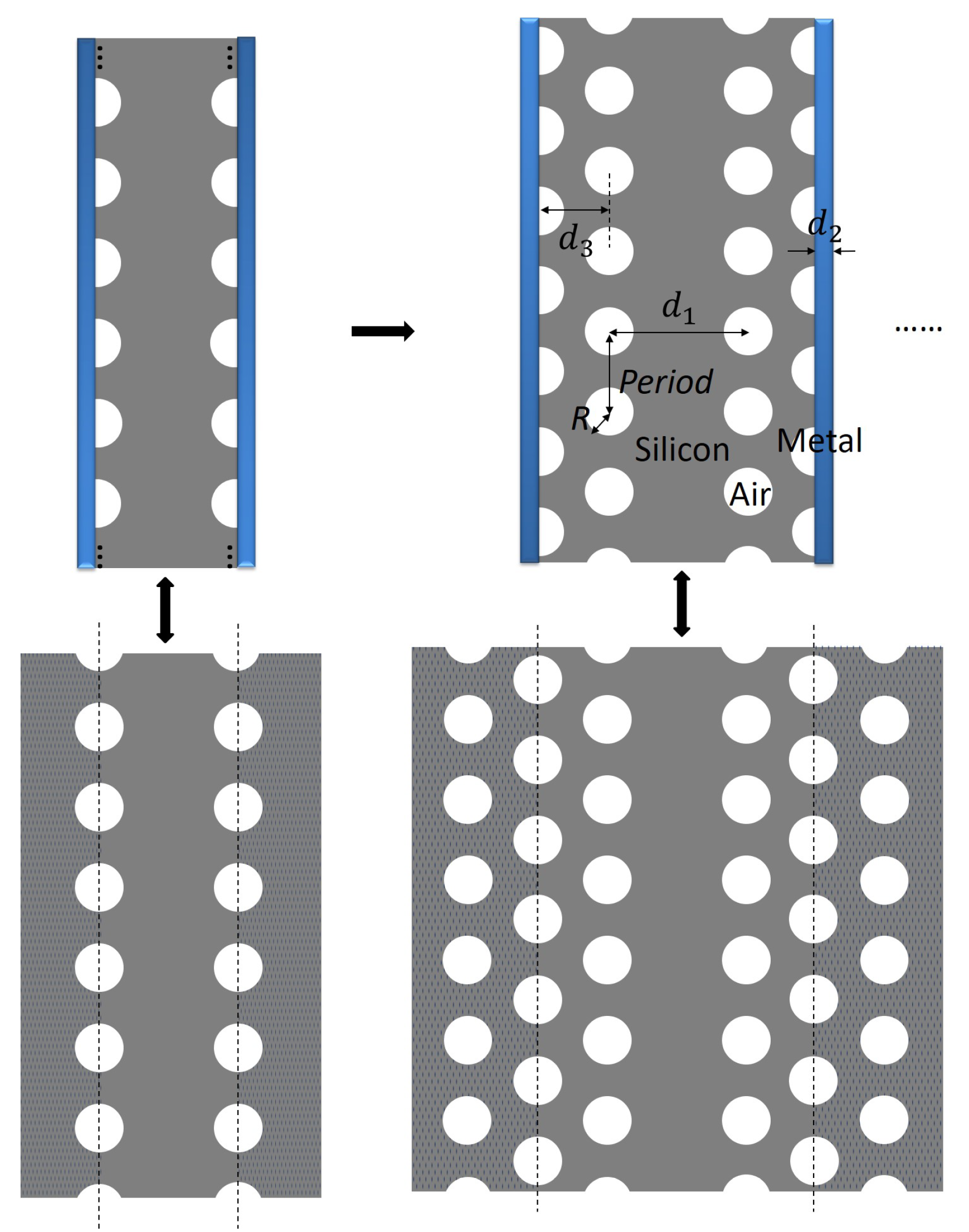
The PhC-like waveguide is formed by introducing a few columns of periodic air holes with one metallic sidewalls on each side of the silicon core of a TE-mode MDM waveguide. The air holes are employed to enhance the mode confinement and to extend the propagation length at the same time. The schematic is shown in
Figure 1, where
and
are, respectively, the distances between the centers of two adjacent air holes in the
x and
y directions,
R denotes the radius of all the air holes. The symbol
denotes the widths of metallic sidewalls.
The real waveguide structures will be fabricated on the silicon on insulator platform. It should be much better to perform the three-dimensional (3D) simulation than the 2D simulation. Because the 3D FDTD simulation is very time consuming (hundreds of hours) due to very large data volume/size and calculation memory, we had to transform the 3D structure simulation into the 2D simulation by using the effective index method [
14], as some authors do for integrated optics and waveguides. In the
z (thickness) direction, it is a sandwich structure of air/silicon/silica. The equivalent refractive index of the
z-direction sandwich structure is firstly calculated, and then is assigned to the refractive index of two-dimensional planar silicon. By means of the effective index method, it realizes the equivalent two-dimensional model for the three-dimensional structure. The confinement/divergence in thickness direction are approximately and equivalently considered in the simulation.
In the processing of the effective index method, the effective refractive indices of the air/silicon/silica structure were obtained as, respectively, and , for the thicknesses of core layer of 1 micron and micron. The relative error is very small, compared with the refractive index of bulk Si of . Therefore, in the following 2D FDTD simulation, we used the effective refractive index of approximately. In addition, due to high index contrast between silicon and air or silica, most of the light field is tightly confined in the silicon layer in thickness-direction. Thus, the divergence in the direction is so small that it has only little influence on simulation result.
Therefore, in the following study, we applied the two-dimensional finite-difference time domain (2D FDTD) method with the boundary conditions for perfect matching absorption in the lateral direction, and the fundamental slab TE mode was considered in the 2D simulations. The grid size of simulation was 5 nm for both
x and
y directions, and the perfectly matched layer PML [
15] absorption boundary with a reflection coefficient below
dB was applied to outside of the waveguide, where there were, respectively
m and
m spacing in
x and
y directions away from the boundaries of the waveguide. To make sure that the PhC-like waveguide can perform the distinguished properties of cm-level propagation length, subwavelength confinement and low crosstalk at telecommunication wavelengths, the geometric parameters of the WG were calculated by the following processes: (1) The parameters of the structure were repeatedly scanned many times, and were finally optimized to be as follows:
m,
m, and
m, with one column of air holes and silver sidewall at each side; (2) The thickness (
m) of silver sidewalls was chosen, because it is much larger than the skin depth (21–22 nm) of silver and is thick enough to screen or isolate electromagnetic crosstalk between adjacent waveguides. In the simulation,
and
were, respectively, the relative permittivities of air and silicon, whose material dispersions on wavelength are very weak for them and can be ignored due to no absorption within the wavelength range of the simulation (1–2
m). However, the metal silver is of strong material dispersion. Thus, its relative permittivity
can be described by the well-known E. Palik model [
16] to satisfy the dependence of refractive index (permittivity) on wavelength in simulation.
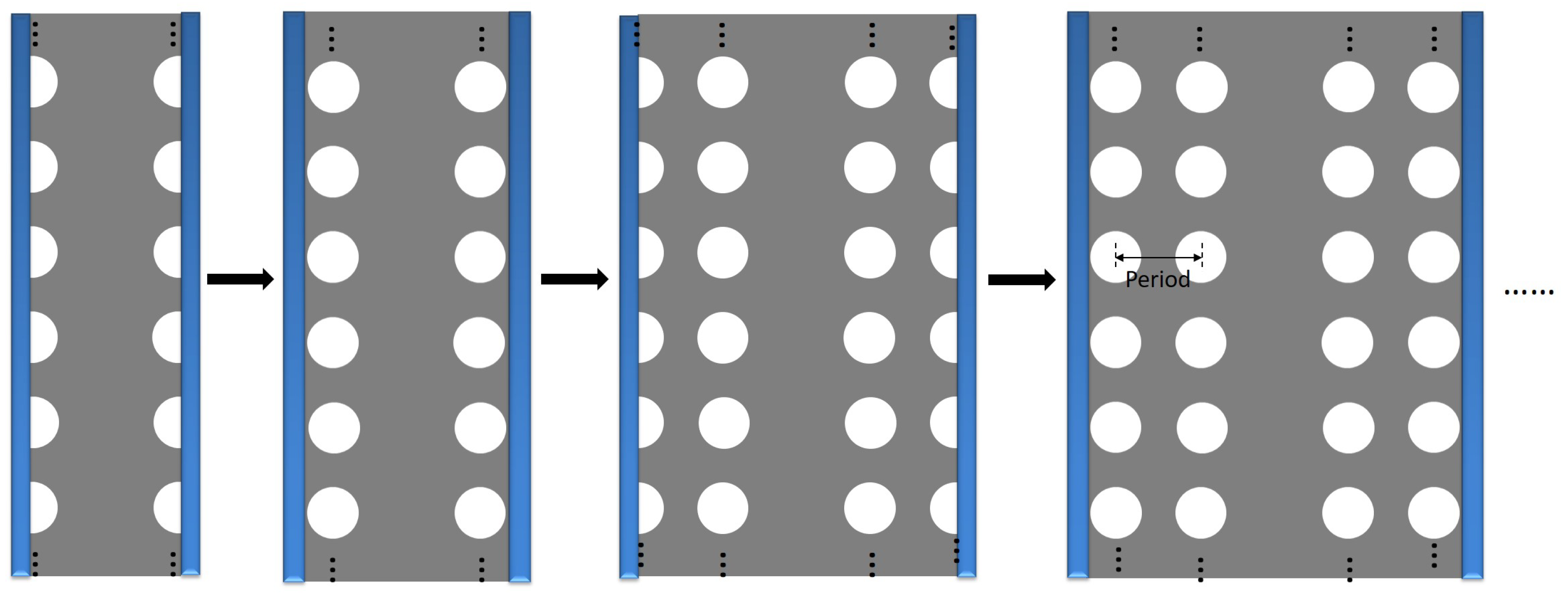
We further discuss performances of different photonic lattice structures with different column numbers of air holes on both sides of the waveguide. For hybrid waveguides with multiple columns of air holes, there are typically two types of lattices of air holes in the lateral direction. One is a triangular lattice of circular air holes (the number of air hole columns to be , respectively, on both sides of the waveguide), while the other one is a square lattice (, respectively). When the air-hole column number is 0, the waveguide is a pure MDM waveguide. As the number of air-hole columns continues to increase, the hybrid waveguide tends to be a PhC-like line-defect waveguide. The transmittance (normalized power) is defined to be , where and are, respectively, the input and output powers of the waveguide. The corresponding transmission spectra are recorded by power monitors.
2.1. A Triangular Lattice of Circular Air-Holes
For the triangular arrangement model, the two adjacent air holes are staggered by along the longitudinal direction, and the lateral distance is , so that the adjacent three air holes are arranged in an equilateral triangle, and thus expanded to have different waveguide structures because of the multiple rows of air holes.
2.1.1. Performance of PHc-Like Waveguides with Different Number of Columns
Figure 1 shows the corresponding waveguide structures, which consist of
columns of air holes at both sides, respectively, with two narrow metal walls as the waveguide claddings and the basic parameters of photonic crystal-like waveguides are also briefly described. The light diffusing or leaking from the waveguide core firstly passes partly through and is partly scatted by the air-hole structure in planar direction. After being near-completely reflected by the metal, the transmission part passes partly through and is partly scatted by the original air-hole structure again, which scatters (or reflects) and transmits the light twice. The effect is similar to doubling the structure of the air holes, which is similar to the symmetrical imaging of a mirror [
17] in Geometrical Optics (the analog of the mirror image). Therefore, due to the twice scattering and transmitting effect, the waveguide structures of
columns with a metal layer on each side are approximatively equivalent to the structures of
columns on each side without metal layer.
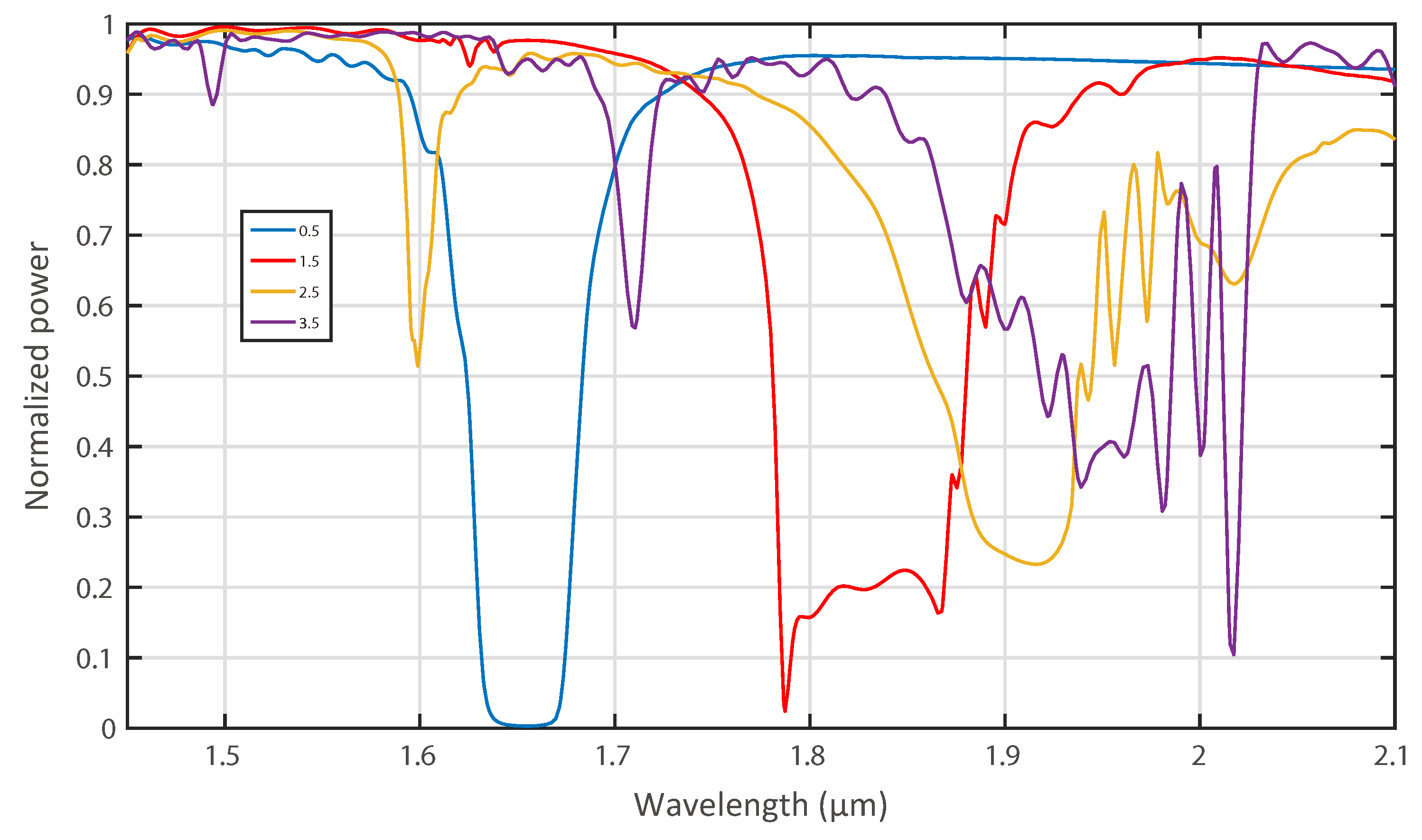
Figure 2 shows the transmission spectra of the waveguides with different columns of air holes. When the number of columns on each side is
or 1 (the equivalent column number of 1 or 2), the transmission spectrum is of the transmission spectrum of side-corrugated Bragg grating on a waveguide [
18]. When the number of columns is
(the equivalent column number of 3) or more, the spectrum starts to show more fine features, and more than one stop band occurs. It reveals that, as the number of columns increases, the guiding mechanism changes from the effective index contrast of the column region (which improves light confinement) into the multiple scattering (or reflection) of 2D periodic air-hole structure in longitudinal and transverse, and coherent or canceling interference happen in different wavelengths. All spectra can maintain low transmission loss over a certain wavelength range; in particular, one can find that in the wavelength range of 1.45–1.58
m, highly efficient transmission can be maintained regardless of the number of columns of air holes on both sides. For this reason, the wavelength of
m is chosen in the following numerical investigation, and the results are shown in
Figure 3.
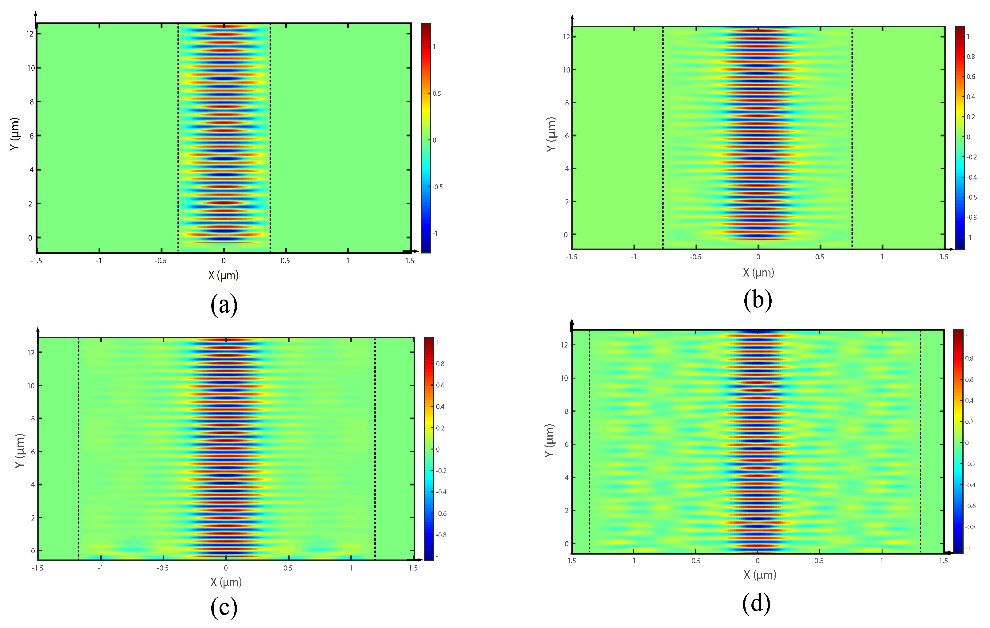
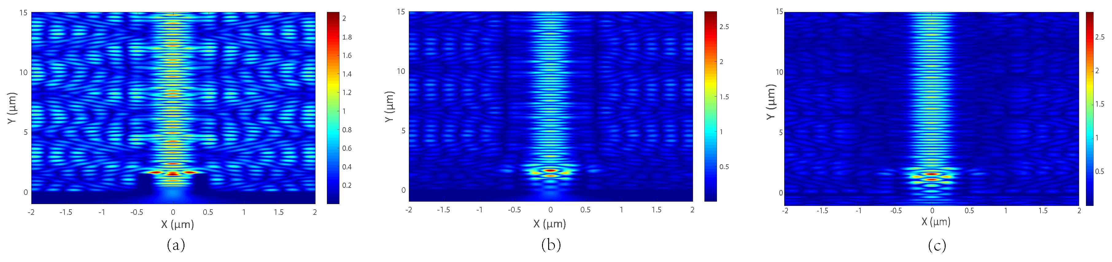
One can see that the waveguide mode is close to the two metal walls for the case of
column of air holes on each side, as shown in
Figure 3a. The waveguide mode is mainly confined by only
column of air holes and metallic sidewalls on both sides, resulting in very large propagation loss (up to
dB/cm), as shown in
Figure 4 below, due to the ohmic absorption of the metal. As the number of air-hole columns increases, the field confinement of the waveguide is strengthened, which means the field is more focused or distributed in waveguide core and fewer amount of light contacts with the lossy metal. Therefore, the propagation loss decreases with the increase of columns of air holes and approaches toward zero, because the light-metal interaction becomes weaker, as shown in
Figure 3 and
Figure 4.
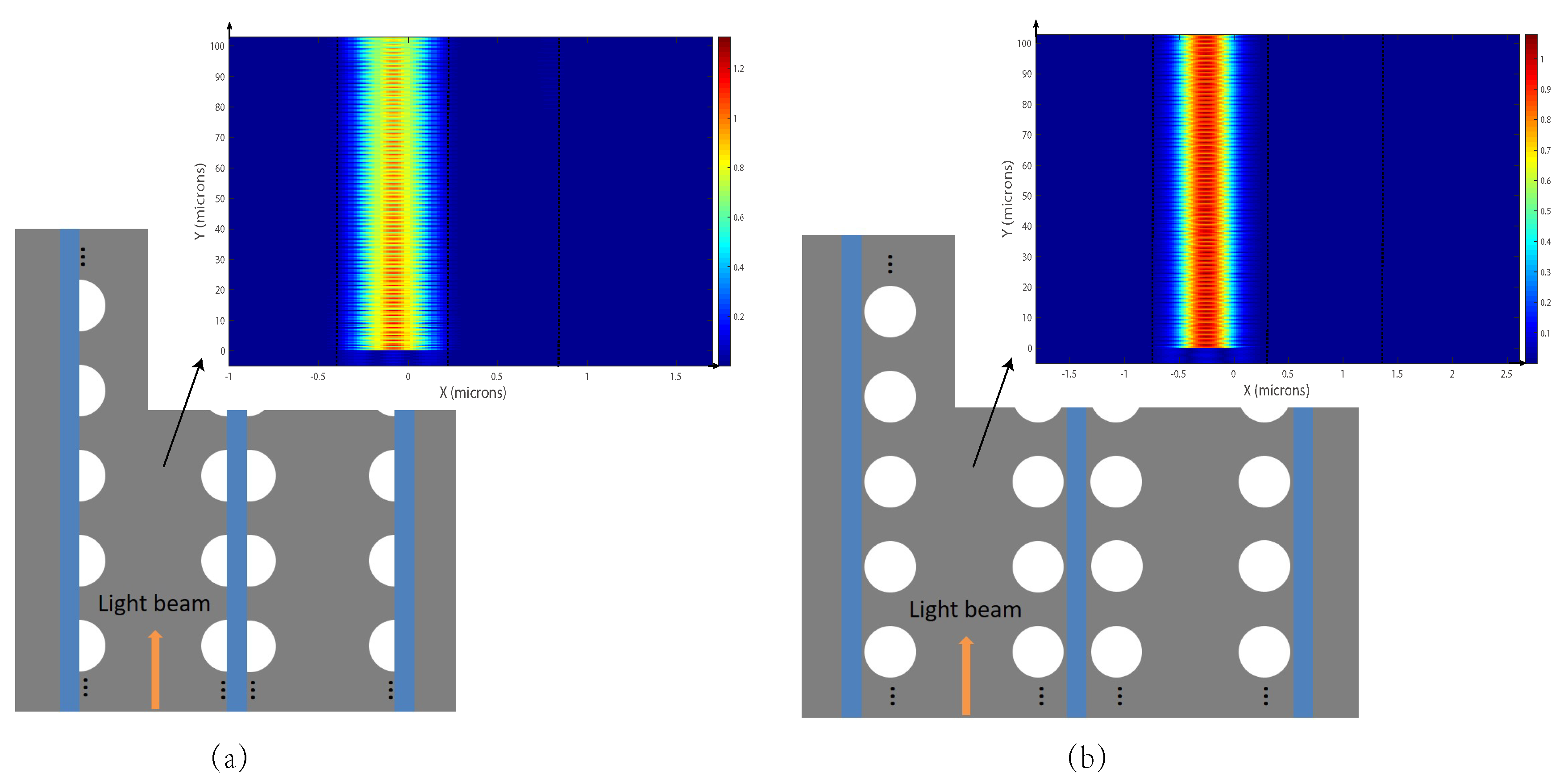
Figure 5 shows simulation results of light propagation in the waveguides of air holes without metallic sidewall, in order to demonstrate the effect of metallic sidewalls. It can be seen that part of light wave leaks from the core and spreads outside. The propagation losses of the waveguides with
,
and
columns of air holes without metallic sidewall are calculated to be, respectively
dB/cm,
dB/cm and
dB/cm from the simulation at
m wavelength, which are much larger than the values of propagation losses shown in
Figure 4. Basically, there are two kinds of photonic crystals. One is the structure of periodic dielectric cylinders with complete photonic bandgap [
19]. The other is the structure of a solid dielectric filled peripherally with periodic air holes, most of which only has partial bandgap. Our waveguide is the combination of the latter with an MDM structure. Ohmic absorption of light on metallic sidewalls and then the waveguide loss can be reduced by introducing only a few periodic air holes between the core and metallic sidewall to effectively weaken the light–metal interaction.
2.1.2. The High Isolation of Photonic Crystal-Like Waveguides
Because isolation or crosstalk between adjacent waveguides determines how closely two waveguides can be laterally placed in the integrated plane, the isolation versus the width of the common silver sidewall was examined. The isolation (or crosstalk) between adjacent waveguides determines how closely two waveguides can be laterally placed in the integrated plane. The isolation is defined to be , where and are the powers monitored at the output ports for the channel waveguide and its adjacent waveguide, respectively.
In
Figure 6, we give examples of two closely spaced waveguides with
and 1 column air holes, respectively, and with a metallic sidewall width of
m between them to show the isolation between left and right waveguides. The light beam is launched at the input port of each left waveguide at the wavelength of
m. It can be seen that the beam propagating along each left waveguide can be well confined and the right waveguide is well isolated from the left one. The two silver sidewalls of the proposed waveguide can be approximately treated as two perfect mirrors, which can form mirror images of the realistic silicon core to equivalently double column number of air holes. The simulation of two adjacent waveguides shows the isolation between them is
dB for the propagation distance of
m in the waveguide with
column air holes at the wavelength of
m, as shown in
Figure 6a. The width of 100 nm far exceeds the skin depth of the silver (∼21 nm at
=
m). Therefore, the width of 100 nm is safe enough for silver wall to achieve high isolation. If the number of air-hole columns increases, the isolation will be better, as shown in
Figure 6b.
2.1.3. The Propagation Loss and Integration Density Versus Column Numbers of Triangular Lattice Air-Holes Waveguide
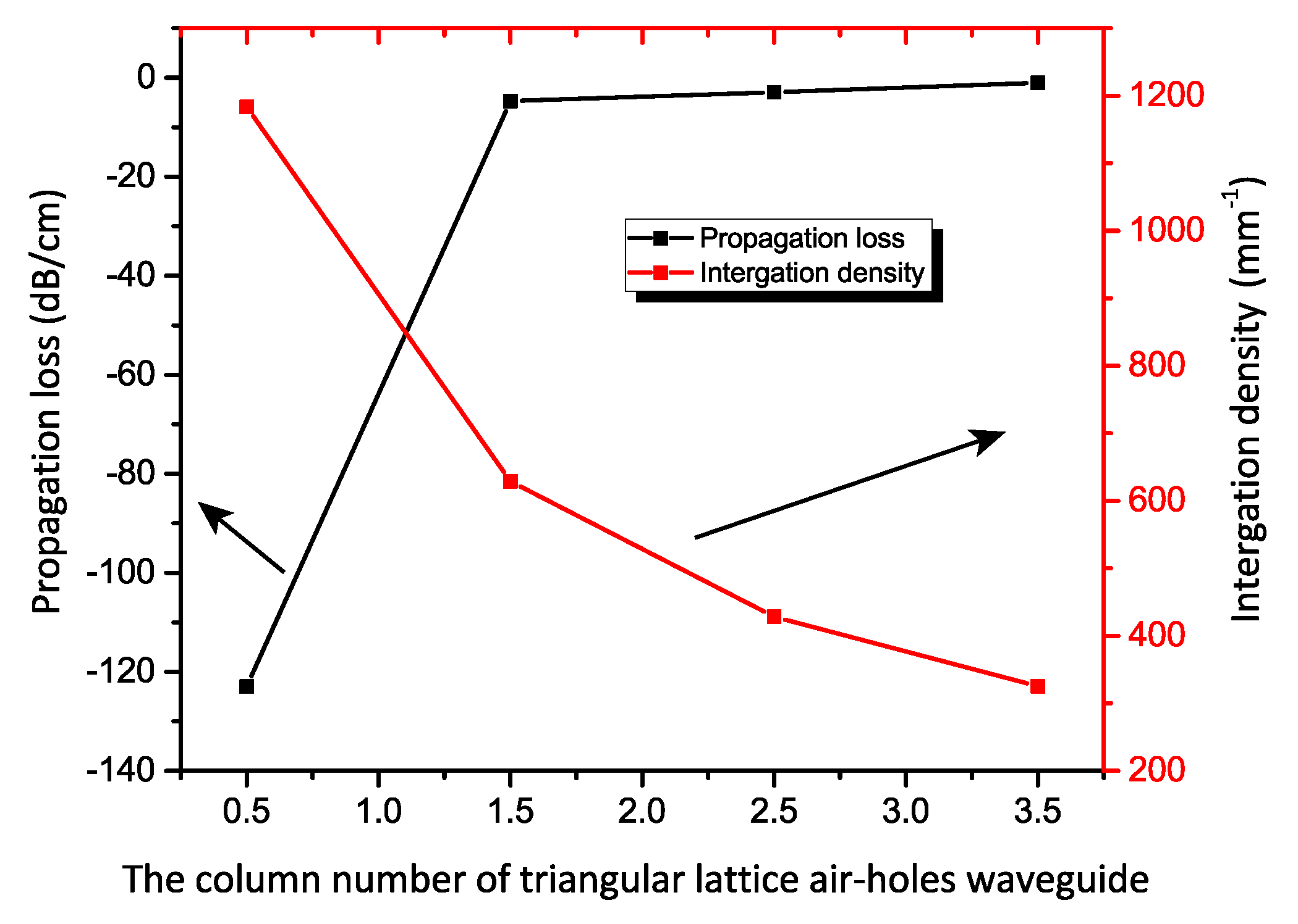
At the wavelength of
m, we obtained the propagation loss from the definition of
, where
and
are, respectively, the input and output powers of the waveguide in 17 periods of air holes at the propagation direction. The loss per length is averaged from the definition of
, where the
is the distance (of 17 periods) between the two monitors in the propagation direction of the waveguide, to obtain the propagation loss per centimeter for the subwavelength waveguides with different column number of lateral air holes, as shown in
Figure 4. It can be seen that the propagation loss is also small in the centimeter-level transmission distance as the waveguide with 1.5 columns of air holes or more. Many micron-scale devices can be integrated in the cm-level waveguide platforms. There are few reports on cm-level waveguide with subwavelength confinement in the integration plane in the literature.
Next, the integration density is defined as the number of parallel-integrated waveguides with high isolation (>30 dB) in one millimeter in the lateral direction, the integrated density is further compared to obtain the optimal performance. As shown in
Figure 4, the integration density decreases for subwavelength waveguides with a larger column number of air holes. Therefore, there is a tradeoff between the propagation loss and the integration density. One can choose different column number of the waveguide for different application requirement. Since the intersection of the loss curve and the integration curve does not fall within the structure range of the triangular lattice waveguide, we continue to explore the square lattice waveguide for the balance between the loss and integration density.
2.2. A Square Lattice of Circular Air Holes
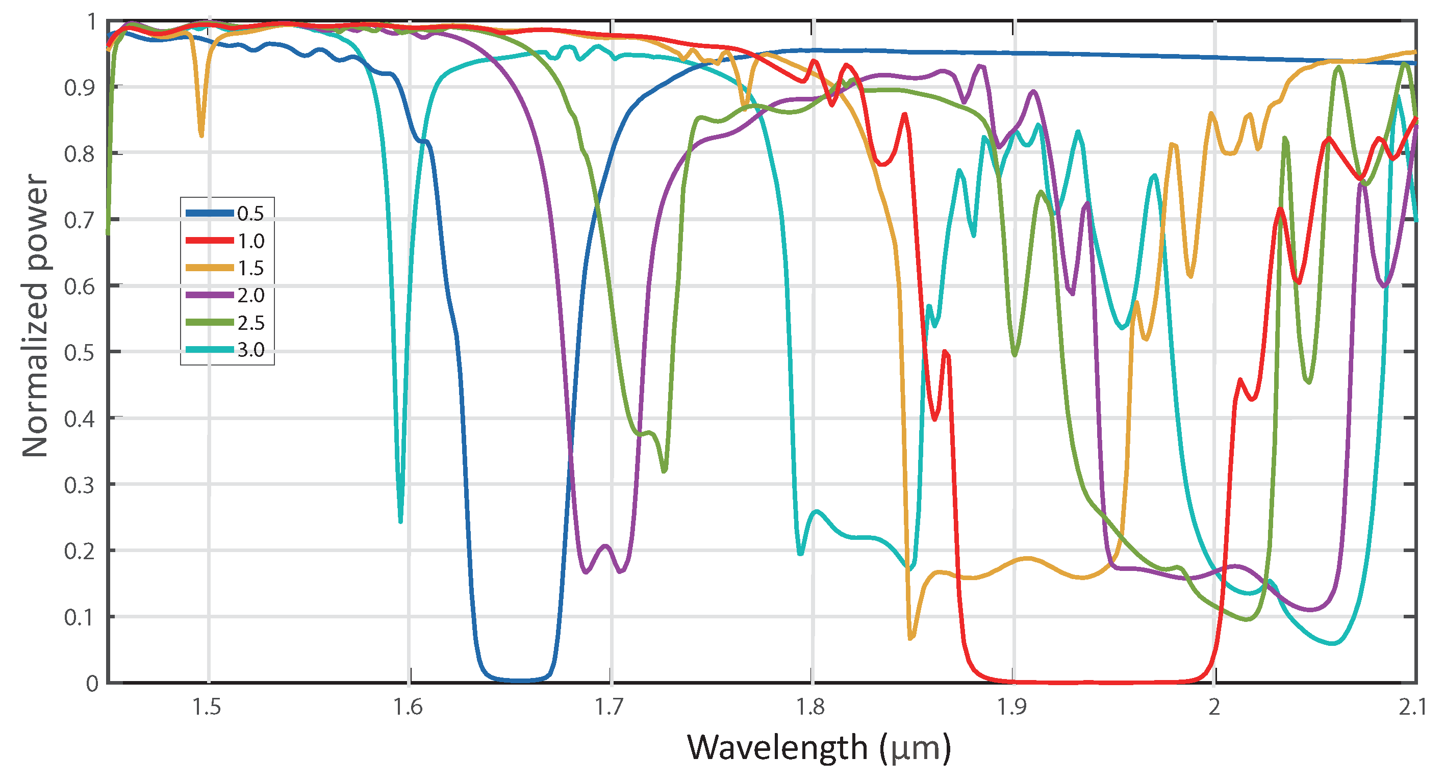
Unlike the triangular lattice structures, the square lattice structures can appear as an integer column.
Figure 7 shows the structures of the PhC-like subwavelength waveguides with the square-latticed air holes, while
Figure 8 shows their spectra.
2.2.1. The Propagation Loss and Integration Density Versus Column Numbers of Square Lattice Air-Holes Waveguide
Figure 9 shows dependences of the propagation loss and integration density on column number of air holes in the square-lattice hybrid waveguide. It reveals that the trends of the propagation loss and integration density of the hybrid waveguide with square-lattice are similar to those of the waveguide with triangular lattice. Similarly, the transmittances of the waveguides are close to 1 around 1.45–1.57
m.
The comparison between
Figure 4 and
Figure 9 does not show a pronounced difference on the trend. Only there is the difference of waveguide width between the structure (
m) with
columns of air holes and the structure (
m) with 1 column of air holes, which brings different integration densities of 629/mm for the former in
Figure 4 and 877/mm for the latter in
Figure 9.
2.2.2. Reflective Performance of the Waveguides
As shown in
Figure 8, one can see that the waveguide with 0.5-column air holes (or with 1-column air holes) has a stop-band (near-zero transmittance) around
m (or
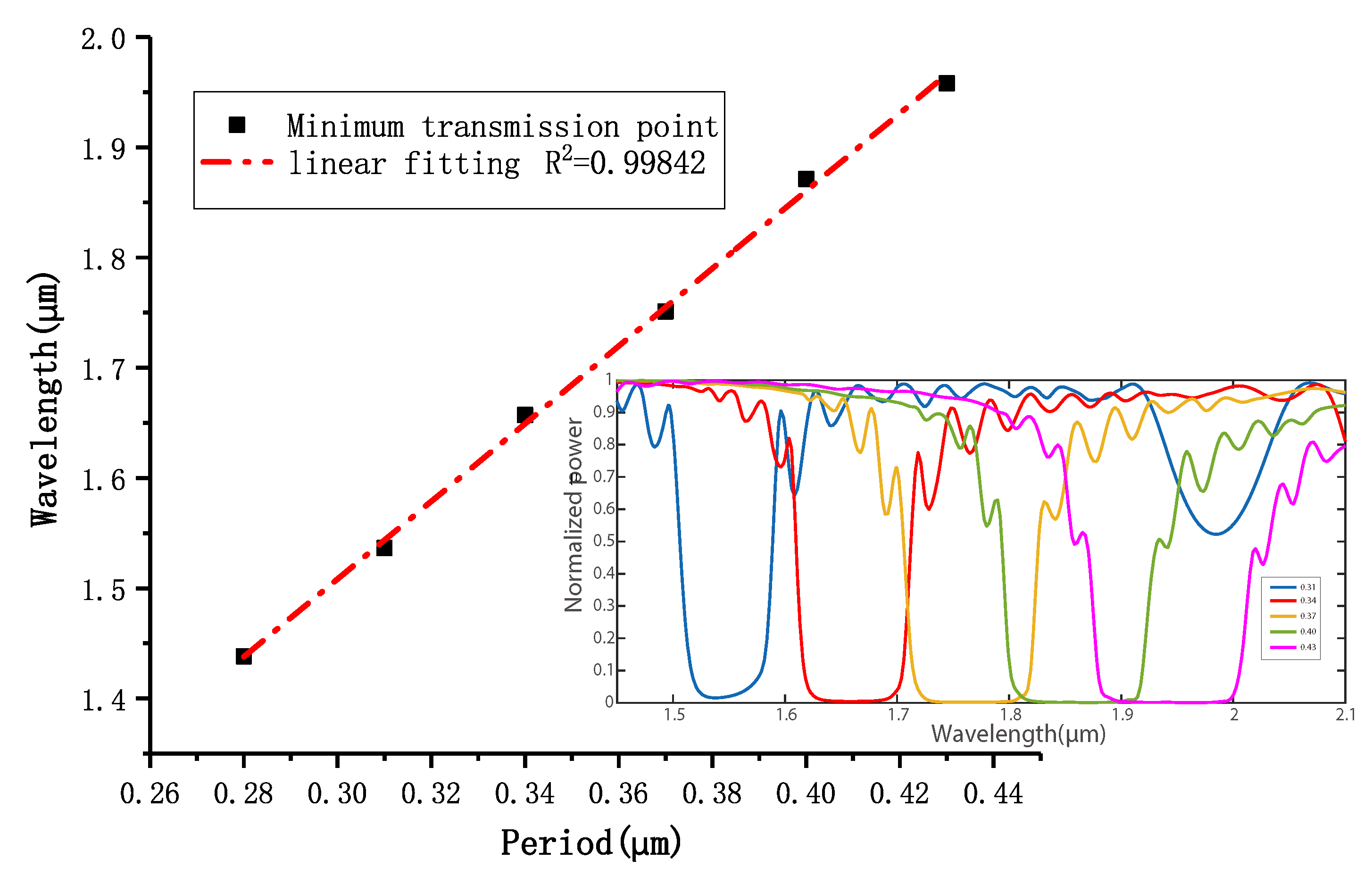
m). According to the simulation result, in terms of wavelength filtering, it can be applied by utilizing its high reflective character. Therefore, we choose the waveguide with one column of air holes to do some studies.
In
Figure 10, one can find that the band gap increases linearly by the increasing of the period of air holes. One can fine tune the peak reflecting wavelength by changing the period. This feature will provide a new pathway for reflection-type wavelength filters.
The study presented in
Section 2 provides systematical investigation of the characters of the waveguides as well as a theoretical basis for subsequent control and application of the waveguides.
3. T-Shaped Splitter Based on the Subwavelength Waveguides
The passive power splitter is one of the fundamental components. It is widely applied in optical switches, wavelength-selective filters, light modulators, etc. [
20,
21]. However, the splitter based on a PhC-like waveguide has not been proposed in the previous study.
At present, there are many types of power splitters, such as dielectric waveguide splitter [
22], photonic-crystal waveguide splitter [
23], plasma metal waveguide splitter [
24,
25] and hybrid structure waveguide splitter [
26]. Dielectric waveguide splitter can only be used at a small splitting angle. Photonic crystal waveguide splitter and plasmonic waveguide splitter can realize the beam splitting at a large angle.
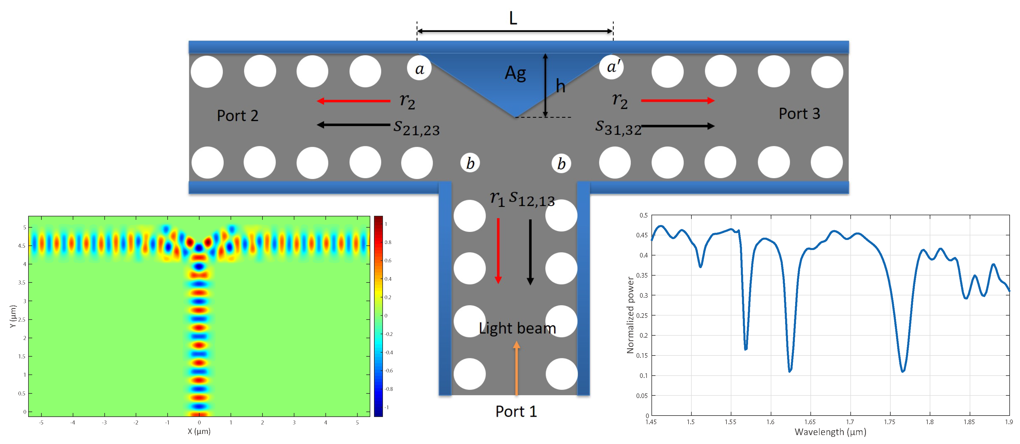
Here, we propose a T-shaped splitter, which can split the light symmetrically with 90 angle and with high efficiency.
Figure 11 shows an optimized structure of a T-shaped splitter. The illustration in the lower left corner is the
field at an incident wavelength of
m.
The T-type splitter can be physically analyzed in the scattering matrix theory [
27] as follows:
where
(i = 1,2,3),
,
and
are, respectively, the reflection and splitting coefficient of the corresponding port caused by the structure; and
and
stand for the fields of incident and output beams at Port i, respectively. Using Equation (1) and the law of conservation of energy for only one input beam of Port 1, one can obtain
, and
. It finally gives
Therefore, to get the maximum energy transmittance of , one has to optimize the reflectivity of the design to be very small, even close to 0. The performance of varied radius and the positions of several air holes on the loss at the branch is simulated, and a triangular metal Ag with suitable L and h is used to achieve high splitting efficiency.
After the optimization, a splitter with a transmission efficiency of 0.422 can be obtained with the parameters of
m,
m,
m (the positions of air holes a and
are deviated from the original position with
m,
m), and
m. It gives an excess loss of the T-type splitter less than
dB. The right insert of
Figure 11 is the spectrum of the T structure. It gives the operation wavelength range (1.45–1.51
m, 1.52–1.56
m) of T-type splitter. If the angle of T-type splitter is changed, it will become a Y-type splitter. One can design a Y-type splitter with an arbitrary angle based on the same optimization process. By adjusting the sizes and positions of the air holes and the size of the metal at the junction, the branching effect can be optimized.
The minimal size of the air holes and the smallest width among the metal walls are, respectively, 130 nm and 100 nm, which are all larger than the resolution (∼5 nm) of a typical electron-beam lithography (EBL) system. The fabrication process of the PhC-like waveguides can be conducted in the following five steps: (1) The EBL system is employed to pattern the ZEP520A spin-coated on a SOI wafer, to define the air holes and metal channels; (2) Reactive-ion etching (RIE) is used to transfer the defined pattern onto the top silicon layer of SOI with C4F8 and SF6 gases. RIE overetching is performed to etch away part of the buried oxide layer just beneath the waveguide core. Then, the remaining ZEP520A is etched away by oxygen plasma; (3) The fabricated wafer is spin coated with a thick layer (at least ∼1m thicker than that of the metal sidewalls) of PMMA, which is defined by a second step of EBL with good alignment, and thus acts as the mask for protecting the waveguide core with air holes; (4) Silver is then evaporated into the metal channels; (5) Finally, the lift-off process is performed to remove the metal above the PMMA mask with acetone.


