1. Introduction
Semiconductor silicon chips are used for various applications, including consumer electronics, industrial purposes, telecommunication, and in the automotive field. Being the second most abundant element on Earth, silicon is a relatively inexpensive material and is highly reliable due to its versatility and physical–chemical properties [
1]. Its thermal expansion coefficient is low compared to most metals, making most of the effects negligible due to thermal shock and fatigue. Silicon is fairly inert under standard environmental conditions, it does not react with most acidic compounds, but reacts with diluted alkalis and halogens, and its electrical conductivity can be tuned by adding small amounts of impurities [
2]. For these reasons, semiconductor silicon remains the core component of many microelectronic devices, it is an essential component of integrated circuits (ICs), the building block of power devices such as computers and smartphones, and it is essential for photovoltaics to manufacture solar cells. In particular, single-crystal silicon is the most widely used semiconductor material in the micro-electromechanical (MEMS) manufacturing and electronic and optoelectronic circuits industry. In addition, the continuous demand for compact and miniaturized devices has increased the need for more functionalities from a single device. This means that today an IC chip is requested to house a larger number of components to support more features. A silicon-integrated circuit chip is realized by embedding and overlaying different elements of a wide variety of materials, each characterized by different elastic and thermal properties. Therefore, it follows that many structural elements, by virtue of their formation processes, exhibit intrinsic stresses. Stress problems are prevalent in silicon technology and become critical, as they can impact the performance of the ICs. For these reasons, understanding the nature and origin of stresses is a fundamental issue. It is strategic to investigate the stresses developed during the assembly process, as a function of the working parameters, using an experimental technique and predictive theoretical models. Raman spectroscopy is an efficient tool to measure residual stress by correlating the effects with the optical change in the materials [
1,
2,
3,
4,
5,
6,
7]. Moreover, it is a nondestructive and noncontact method, characterized by a high spatial resolution, and has already been widely used to investigate silicon, such as in cubic crystals [
8,
9], microelectronic devices [
10,
11,
12,
13], and nanostrips [
14].
Selecting the right substrate materials for the production of microelectronics is one key point in the process. The substrate must be highly reliable, in configurations precisely chosen to meet the needs of a specific application. Several substrate materials are used, which are carefully chosen on the basis of the performances needed to reach, but also following other criteria like safety, environmental impact, economic costs, and process complexity. Organic-based composite materials in polymeric form have attracted considerable attention because they offer the opportunity to produce substrates with multiple customizable functionalities, they cover large areas, and are flexible, lightweight, and are relatively low in cost [
15,
16,
17,
18]. There is an immense scope for the future of flexible organic electronics. However, the current performance and lifetimes of electronic devices based on organic substrates are still lower than those of traditional ceramic or other inorganic materials [
19], such as aluminium nitride or copper. Ceramic substrates are well known for high-temperature electronic integration. Copper substrates are widely used in microelectronics because of the advantageous properties of copper, such as low electrical resistivity, high electromigration resistance, high thermal conductivity, excellent chemical and thermodynamic characteristics, antimicrobial properties, and low cost. A problem with Cu is the tendency to form oxides on the surface; this problem can be overcome using formic acid or formate salts to prevent the formation of oxides, as reported for LED assembled on copper substrates [
20].
The focus of this work is the evaluation of residual stresses on silicon samples that are intended to simulate part of the structure of an optoelectronic device. This study represents an important starting point for the development of optoelectronic devices with characteristics suitable for future industrial production. The aim is to experimentally investigate the stresses induced on the devices during the assembly procedure as a function of different process parameters, such as the physical and chemical characteristics of the involved substrates, temperature, and pressure. The samples examined consist of a silicon chip, with a thickness of 120 μm, soldered under different conditions on copper or alumina (Al2O3) substrates, with a thickness of 1 mm. A stress evaluation was performed, using a micro-Raman spectroscopic technique. Measurements were carried out at room temperature and at different temperatures, ranging from −50 to 180 °C, a temperature range for the use of electronic devices. The results obtained suggest advantages and disadvantages in terms of stress in the use of ceramic substrate over copper substrate and the effect of applied pressure during the assembly process of the samples.
2. Materials and Methods
2.1. Materials and Sample Preparation
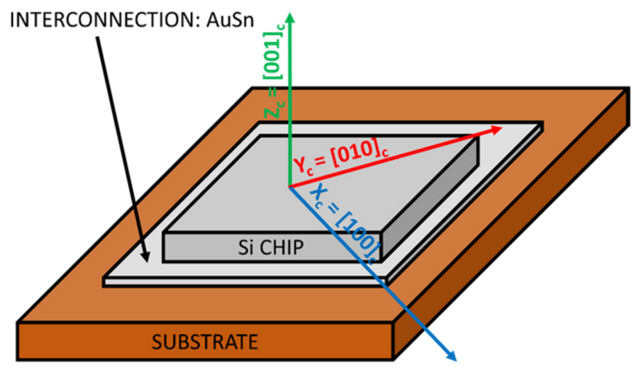
The assembly structure of the developed samples consists of a substrate, above which an interconnection material is located, and a Si chip, which is placed above it, as represented in
Figure 1.
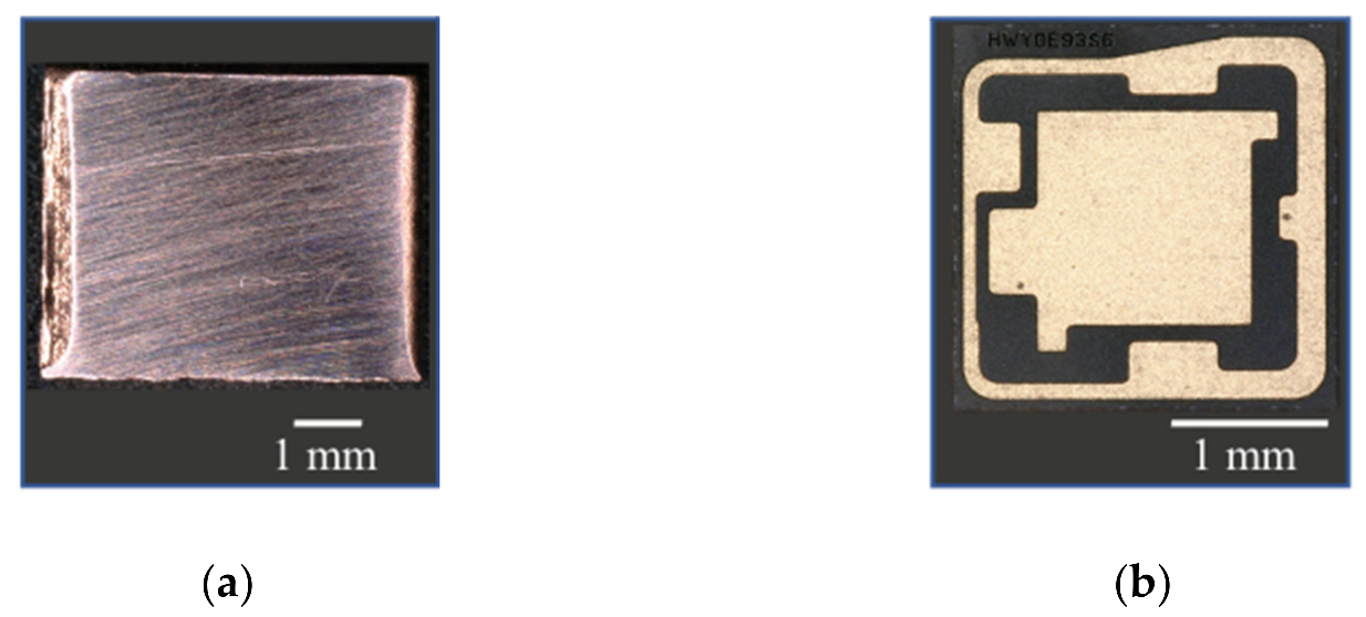
In this work, two types of substrate were adopted: a copper substrate, with dimensions (5 × 5 × 1) mm
3, and an Al
2O
3 ceramic substrate, with dimensions (2.4 × 2.4 × 1) mm
3, covered with gold metallization, reported in
Figure 2a,b.
The copper substrates were mechanically treated first by rubbing the surfaces on abrasive discs with different grains, taking care not to avoid scratches; then they were placed in an ultrasonic bath of 4% hydrochloric acid, and finally in an ultrasonic bath with isopropanol. Ceramic substrates were used without any prior treatment.
Silicon chips were adopted with dimensions 1500 × 1500 × 120 μm
3, (001) oriented, and with gold metallization at the bottom. An interconnection material, for the soldering process, was used to build the devices: it consists of a thin layer of Au80Sn20 eutectic alloy with a thickness of 25 μm [
21,
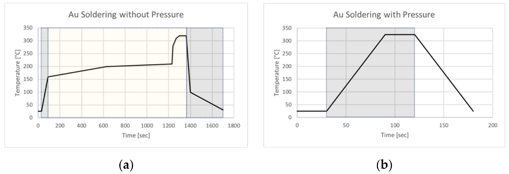
22]. The soldering procedure was carried out following two different working processes, depending on the application or not of an external pressure. All Si-chips were soldered to the substrate using a vacuum-assisted closed reflow oven (Unitemp, RSS-160). For efficient soldering, surface oxides and undesired residuals were removed using formic acid vapor, which has strong reducing effects. The assemblies were prepared at 320 °C, using a bonding time of 80 s (for the samples without additional pressure) and 30 s (for the samples with additional pressure). Several assemblies were prepared to confirm the reproducibility of the experimental results.
Figure 3 shows the temperature profiles in the reflow oven. Before proceeding with the Raman measurements, the final assemblies were optically inspected by a 3D digital microscope (Keyence VHX-900F).
For the samples prepared under pressure, the soldering process was carried out at 5 N, both in air and in N
2 atmosphere, according to the scheme reported in
Figure 3b. Pressure was applied through a Fineplacer bonder (FineTech
® AP2.4 145/FP 145 Pico ma), placing the chip and applying an established pressure perpendicular to the substrate surface by heating and controlling the environment of the system together. The value of 5 N was selected because it represents the maximum applicable pressure to avoid damaging the silicon chip during the assembly process.
The list of all the assembled and investigated samples is specified in
Table 1. Four types of Si chip samples were prepared via a soldering process: samples mounted on Cu substrates, without any pressure (A_AuSn) or using a pressure of 5 N (A_AuSn_p), or on ceramic substrates, without any pressure (B_AuSn) or using a pressure of 5 N (B_AuSn_p). Together with the mounted samples, the starting silicon chip (Si_unmounted) was also analyzed, which has not been assembled to a device.
2.2. Methods
The optical characterization of the samples was performed by recording Raman spectra at different positions on the surface of the chip, in the temperature range from −50 to 180 °C.
The Raman setup consists of a micro-Raman instrument working in a backscattering configuration. An argon–ion laser operating at a wavelength of 514.5 nm (Spectra Physics® Stabilite 2017-output power 1 W) is used as an excitation source. The focalization of the laser was realized through an optical microscope (Olympus® BX 40), equipped with interchangeable lenses 4×, 10×, 20×, 50×, 100×, and with a sample holder table movable in three directions (x, y, z) to regulate the sample position. A camera was coupled to the microscope to observe and correctly choose the area of the sample that was scanned by the laser beam. The typical spot diameter in the focus, working with a 20× objective, was 3 μm. The backscattered radiation was analyzed using a 2400 grid spectrograph and converted into an electronic signal by a nitrogen-cooled charge coupled device (CCD). A temperature controller (Linkam® THMS600) was used to conduct micro-Raman measurements at specific temperatures, where a modified atmosphere with 100% nitrogen was created to avoid problems due to water in the chamber.
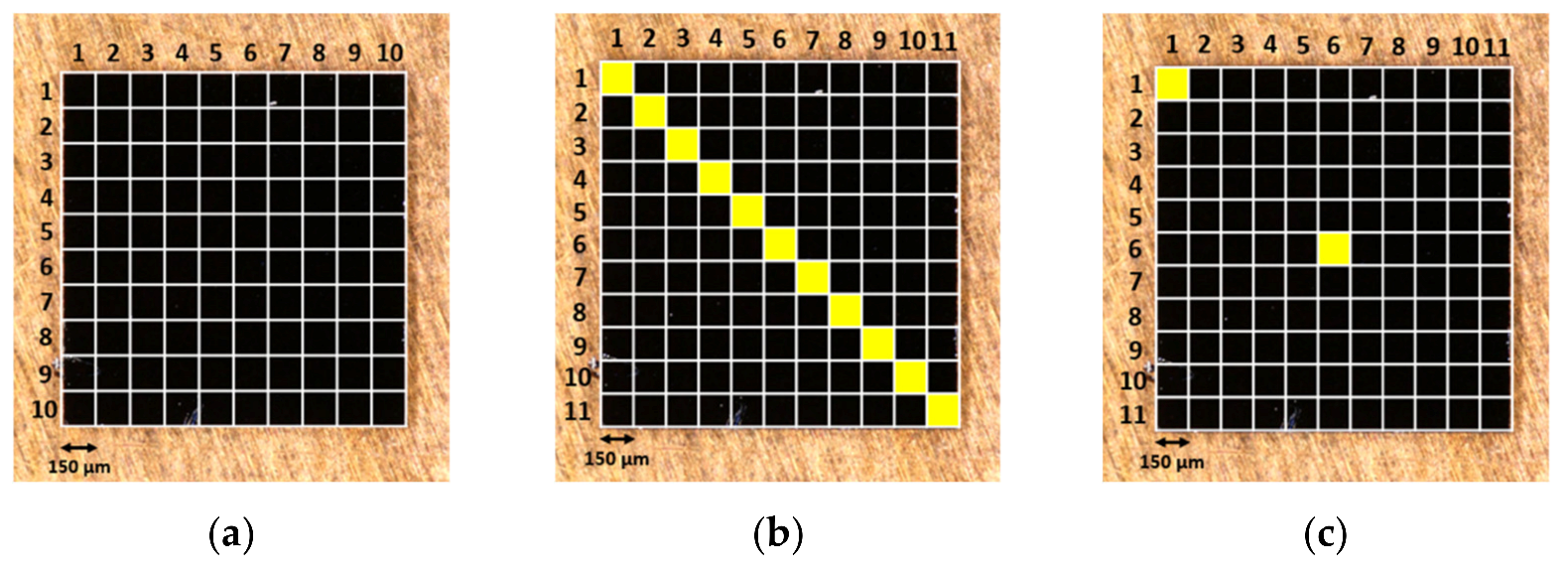
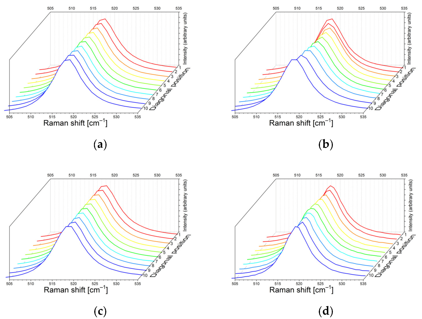
The Raman signal of the samples was measured by mapping the surface of the chip in 10 × 10 positions (reported in
Figure 4a) or by detecting the signal along the diagonal in 11 positions (
Figure 4b) or in two defined positions, corresponding to the corner [1, 1] and the central [6, 6] positions of the chip (
Figure 4c). In all cases, the instrument was set to ensure that the Raman signal was recorded in the central position of each squared area of the desired location.
Each point was recorded using the 20× lens and setting the software with an acquisition time of 5 s. The final spectrum was obtained by averaging five repeated measurements. The slit of the spectrograph was set at 40 μm and kept constant during the analysis of all samples. The input power of the laser was set at 40 mW.
The Raman spectra were acquired at different temperatures, ranging from −50 to 180 °C, using the temperature controller: starting from −50 °C and raising the temperature to 180 °C, waiting 5 min at a constant temperature before signal acquisition, and vice versa, starting from 180 °C and cooling to −50 °C.
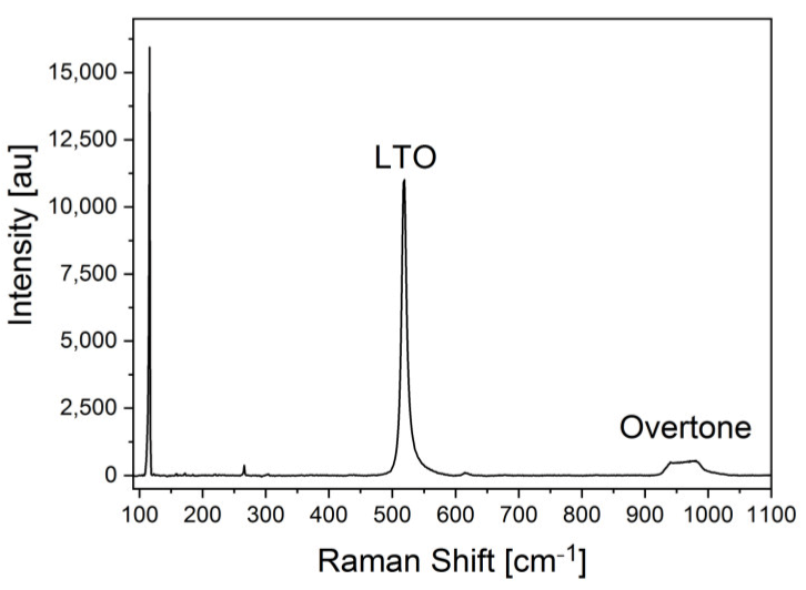
To ensure a correct calibration of the spectrograph, we used the Raman signal from a standard commercial silicon wafer. Moreover, all the spectra of samples were normalized with respect to a plasma line signal, to ensure that the position of the band of interest is not affected by instrumental errors. All of the collected Raman spectra were interpolated with a Lorentzian function to determine their parameters, such as area, intensity, amplitude, and peak position.
2.3. Determination of Stress from Raman Spectra in Si
The frequencies of the Raman modes are affected by thermomechanical strains or stresses. Raman measurements are used to quantify the local residual stress of Si, using the secular equation of Equation (1):
where
p,
q and
r represent the deformation potentials, which are material constants, and
are the strain phonon tensor components along each direction [
23,
24], related to the strain tensor (
σ) through the Hooke’s law
.
are the elastic compliance tensor elements of silicon, reported in
Table 2.
From the eigenvalues
(
j = 1,2,3), it is possible to calculate the difference in Raman frequencies for each mode in the presence (
) and in the absence (
) of stress:
or
Given the values of
,
,
p, and
q, it is possible to solve the secular matrix of Equation (1). The biaxial stress along the [100] and [010] directions (
xy plane, see
Figure 1), for back scattering from a (001) surface, will be
Consequently, the biaxial stress values can be calculated using Equation (4).
In general, a Raman frequency value higher than the stress-free frequency indicates compressive stress in the sample, while a Raman frequency value lower than the stress-free frequency indicates tensile stress [
24].
The evaluation of the stress induced in the chips by the assembly process can be performed considering the unmounted chip as a reference (providing the value of ) and measuring the position of the Raman shift of the assembled samples.
4. Discussion
The biaxial stress values of silicon have been calculated from Raman data with the equation
. A Raman frequency greater than the stress-free frequency indicates compressive stress in the sample, while a Raman frequency smaller than the stress-free frequency indicates tensile stress [
7,
10,
25].
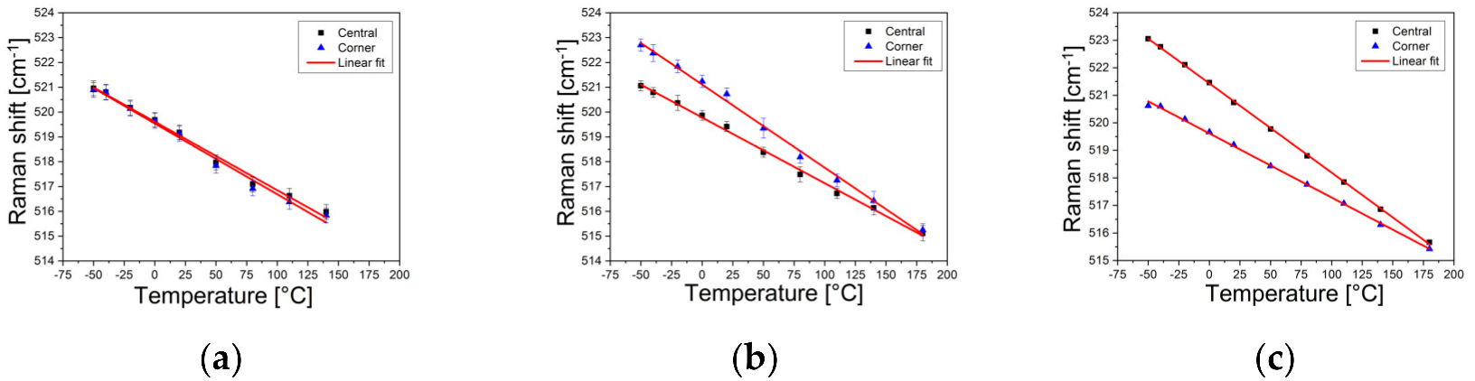
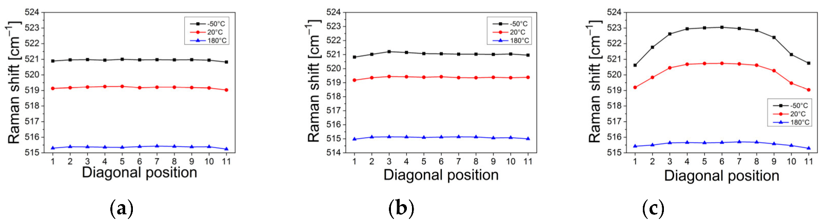
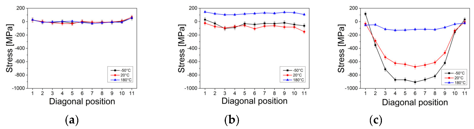
The stress values of the Si samples evaluated along the diagonal positions at −50, 20, and 180 °C, from Raman spectra, are reported in
Figure 10. To evaluate the stress values of the assembled samples, the Raman frequency of the unmounted sample is assumed as the reference value:
is the Raman shift value of the j-peak of the sample, while
is chosen as the Raman shift of the unmounted sample relative to the same position on the map, in order to relate the measured stress only to the assembly process, that is, to neglect the intrinsic stresses that are inevitable in the samples. Instead, the stress of the unmounted chip is calculated by considering as a reference the internal value obtained from the average Raman shift of the entire position of the sample in the unmounted sample. The negative sign indicates compressive stress.
The experimental data show a compressive stress, whose values vary in a range of 1 GPa when the assembly is at high temperature (180 °C) or low temperature (−50 °C).
The figure shows that the magnitude of stress in the sample prepared under pressure is much lower than in the sample prepared without the use of an additional pressure of 5 N. At first sight, the conclusion would be that the effect of the pressure during soldering of the transition AuSn layer could be helpful, because for the assembly without pressure, the Raman signal of the Si peak changes strongly, in comparison to the signal of unmounted Si. Further measurements were carried out to check the interconnections, in particular, those for the cross-section analyses of the assemblies have revealed that the Si chip was not properly soldered to the substrate, i.e., the use of the pressure of 5 N was a disadvantage on these samples. Studies in this direction are still in progress.
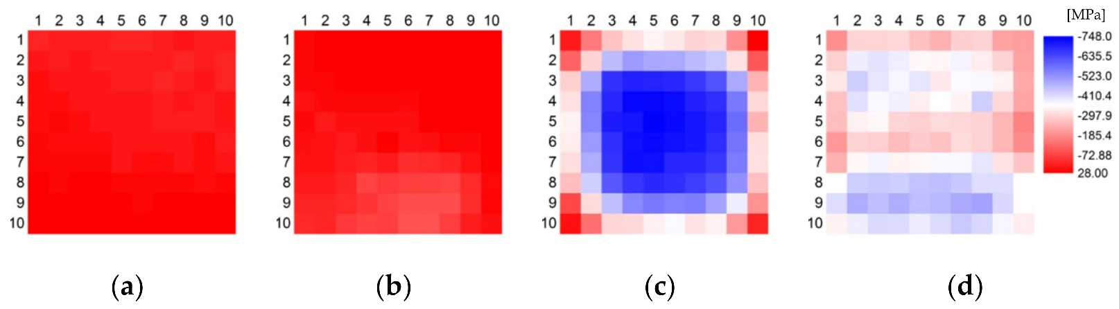
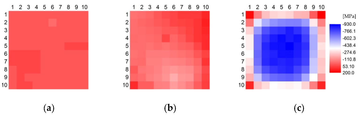
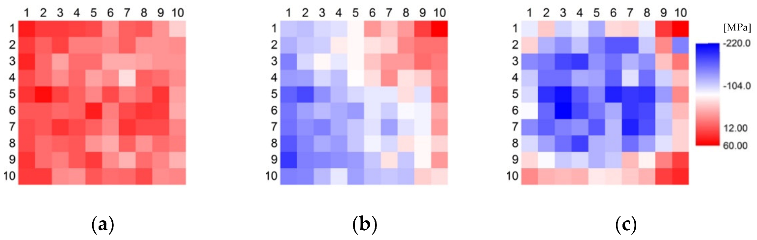
Similarly, the stress distribution of the different samples was determined from the Raman mapping data. Color maps, in
Figure 11, report the stress values of the Si samples, determined on the entire surface of the samples, at 20 °C. A_AuSn is the most stressed sample, with a variation of 775 MPa on the surface. The stress map of the B_AuSn sample shows the highest variation on the total area equal to 329 MPa, a value that is lower compared to the corresponding sample assembled without pressure on the copper substrate.
Figure 12 and
Figure 13 report the stress values of the Si samples, on copper substrates, determined on the entire surface of the samples, at −50 and 180 °C, respectively. The maximum stress is observable at low temperature on A_AuSn: it reaches a value of −928 MPa and is highly symmetric.
Figure 11c,
Figure 12c and
Figure 13c show an unstable stress distribution. This can be correlated with mechanical defects after the soldering process. Cross sections of the samples confirmed the experimental results that the samples had cracks within the solder joint. An alternative method to test the integrity of the solder joint is transient thermal testing, which is a nondestructive tool [
27]. It is worth also recalling that samples with cracks detected by Raman spectroscopy and confirmed by transient thermal analysis and cross section can still have functioning electric contacts, as demonstrated with high power LEDs, which passed the light-on test [
28]. The Raman results of the current study suggest the high potentiality, accuracy, and precision of this optical spectroscopy to estimate the quality of samples.
These results are compared in
Table 4,
Table 5 and
Table 6, reporting the overview of the maximum, minimum, and average values of the Raman shift and stress for each sample, at different temperatures: −50, 20, and 180 °C.
All data are reported with their respective uncertainties obtained from the Lorentzian fit of the peaks. In all tables, the highest variation in Raman shift and stress calculated on the chip surface at the three temperatures is also reported. The errors in the stress values are obtained with the quadrature propagation method.
Considering the unmounted sample (
Table 4), as expected, the position of the peak does not change significantly on the surface when the temperature is constant: this reflects that the unmounted sample presents only weak stress values, randomly distributed on the area of the chip, which fall in a range slightly higher than 100 MPa. From the calculation of the uncertainties of the stress values, it emerges that the measurements show stress values of the same order of magnitude as the calculated errors. This fact agrees with expectations: since the unmounted samples are used as zero-stress reference materials, low-stress values around zero are expected. These values represent the starting point for calculating the stress of the other samples developed during the assembly steps.
The A_AuSn_p sample (
Table 5) shows higher stress variations on the whole surface at −50 °C and at room temperature, while the A_AuSn sample (
Table 6) shows the highest variations at all temperatures. In A_AuSn_p, the peak positions change slightly from point to point on the diagonal, giving asymmetric stress distributions and presenting a region of compressive stress on a side area of the chip. At room temperature, the highest variation in Raman shift on the entire surface is 0.30 cm
−1, which is only slightly higher than that of the unmounted sample. This value corresponds to a variation in stress of 171 MPa. The situation is different with sample A_AuSn: the Raman shift and stress variations over the surface at room temperature are higher than in the other cases: they reach values of 1.88 cm
−1 and 775 MPa, respectively. The stress distribution developed along a diagonal clearly shows the predominance of tensile stresses, higher (in absolute value) in the center of the chip. It increases (in absolute value) with decreasing temperature, particularly in the central area.
The A_AuSn sample displays only tensile stresses (negative values); meanwhile, the A_AuSn_p shows compressive stresses (positive values) at 180 °C and tensile stresses at −50 °C and at room temperature. Further measurements to check the interconnections have revealed that the assembling process was not sufficiently efficient under the pressure of 5 N, because the Si chip was not well soldered to the substrate. Therefore, the initial considerations of the phenomena of weak stress must be reconsidered. Investigations in this direction are underway to understand the effect of applied pressure on the assembly process.
Raman shift profiles at the same sample position recorded at different temperatures show a linear trend with slightly different slope values for the three samples. Therefore, it shows that the effect of temperature has different repercussions on the samples depending on their stress values. In particular, a difference in the variations in the stress values, along the diagonal, from −50 to 180 °C is found, particularly for the A_AuSn sample. At high temperatures, the stress is significantly lower than at the other temperatures. This fact can be explained by considering the assembly process and the materials involved in the process.
The residual stresses in the mounted samples are mainly due to thermal mismatch due to the different thermal expansion coefficients, reported in
Table 7, of the materials involved.
The working conditions of the soldering process reach a temperature of approximately 320 °C. At this temperature, the AuSn interconnection layer is melted and is in contact with a dilated substrate and a dilated chip. During the cooling process, the materials shrink differently according to their thermal expansion coefficients, and the further we recede from the highest process temperature, the more the effect of the different thermal expansion coefficients increases, accentuating the stress on the device. In particular, since the copper substrate has a higher thermal expansion coefficient than silicon, it contracts more than the chip, causing the chip to be more susceptible to tensile stresses.
The measurement temperature of 180 °C represents a value closer to that of the soldering, which means that the materials are characterized by geometric distortions between molecules and intramolecular forces similar to what they have during the assembly process. Furthermore, at 180 °C the Si atoms in the lattice are much more mobile and can easily adapt to the new conditions to which the system is subjected. It results in low variations in the stress on the materials.
The pressure applied during the assembly plays a crucial role in the results: the difference in stress is clearly evident by comparing samples mounted with and without pressure and needs to be further investigated. The pressure may influence the dynamics of the interconnection layer by affecting the voids in the AuSn alloy and the compactness of the conductive layer, influencing the stress of the active layer. In any case, from these measurements it clearly emerges that Raman spectroscopy can be used as a valuable tool to understand the efficiency and quality of the interconnection process.
The results of the analysis on sample B_AuSn, consisting of a silicon chip soldered on a ceramic substrate, are reported in
Table 8. They suggest a lower Raman signal shift along the sample surface than for the same sample assembled on a copper substrate. This result can be easily explained by considering the thermal effect: comparing the mismatch of the linear thermal expansion coefficients of silicon and alumina with the mismatch between silicon and copper, it is observed that for the alumina substrate it is about half as much as for copper. This means that the thermal mismatch generates only weaker stresses.
5. Conclusions
A crucial point in the realization of devices with high performance, reliability, and durability is the evaluation of the mechanical properties of the materials that make up the device itself and are necessary for its assembly. Internal stresses can deform the microstructure of the device and occasionally destroy it. The aim of this work was to investigate the stresses induced in silicon devices during the assembling process as a function of the different assembly parameters, i.e., the physical–chemical characteristics of the involved materials, temperature, and pressure.
Silicon chips soldered with AuSn alloy on copper substrates demonstrated differences in stress values and distributions, depending on the experimental parameters of the assembly process. The stress distribution observed on the assembly on the copper substrate, obtained without additional pressure, depends on the temperature: at 180 °C, no stress is observable, while at 22 °C a compressive stress is developed in the center of the assembly with a maximum value of −700 MPa, which reaches −1 GPa at −50 °C. Indeed, from corner to center, a maximum variation in the Raman band of 1.8 cm−1 is recorded, corresponding to a maximum stress of 900 MPa. These samples present a stress distribution with a symmetric profile with respect to the central area of the chip. In contrast, the samples assembled under pressure conditions of 5 N showed very weak stress values due to inefficient interconnections.
The silicon chip assembled on a ceramic substrate without pressure turned out to be extremely interesting. Even in the absence of pressure, the sample did not show a large shift in the Raman position indicating a low stress: it reaches in the central region a compressive stress of 329 MPa, a value that is lower if compared with the corresponding sample assembled on the copper substrate.
AuSn solder, with a eutectic temperature of 280 °C, is a very promising material for the microelectronic industry, because it shows excellent shear strength and good resistance to oxidation and corrosion. Because intensive studies are ongoing to optimize lead-free soldering, the properties of AuSn solder make it useful in high-performance optoelectronics, power electronics, MEMS sensors, and other various applications. However, Raman measurements show high stress on samples assembled with this material, and this problem must be considered to improve the mechanical reliability of the bonded joints. Studies on sintering are ongoing as an alternative to soldering.


