Article

Combined Influence of Gate Oxide and Back Oxide Materials on Self-Heating and DIBL Effect in 2D MOS2-Based MOSFETs

by
Atabek E. Atamuratov
1,*,
Khushnudbek Sh. Saparov
1,
Ahmed Yusupov
2 and
Jean Chamberlain Chedjou
3
1
Department of Physics, Urgench State University, Kh. Olimjan Str., 14, Urgench 220100, Uzbekistan
2
Department of Electronics, Tashkent University of Information Technologies, A. Temur Str., 108, Tashkent 100200, Uzbekistan
3
Department of Smart System Technologies, University of Klagenfurt, 9020 Klagenfurt, Austria
*
Author to whom correspondence should be addressed.
Appl. Sci. 2023, 13(10), 6131; https://doi.org/10.3390/app13106131
Submission received: 10 April 2023 / Revised: 8 May 2023 / Accepted: 15 May 2023 / Published: 17 May 2023

Abstract

:
In this paper, degradation effects, such as self-heating effect (SHE) and drain-induced barrier lowering (DIBL) effect in 2D MoS2-based MOSFETs are investigated through simulations. The SHE is simulated based on the thermodynamic transport model. The dependence of the DIBL effect and the lattice temperature in the middle of the channel on the gate length is considered for transistors with different gate oxide and back oxide (BOX) materials. The effects of Al2O3 and HfO2 as gate oxide and SiO2 and HfO2 as BOX materials are compared. Transistors, in which the channel is fully and partially (i.e., just below the gate) covered by a gate oxide, are considered. It is shown that the transistors with Al2O3 as gate oxide and SiO2 as BOX materials have higher immunity to DIBL effect and transistors with HfO2 as gate oxide and HfO2 as BOX materials have higher immunity to SHE.

1. Introduction

In accordance with some viewpoints, the scaling of silicon-based planar MOSFETs has approached its physical limit. However, according to some other outlooks, there is still an opportunity to continue size scaling of MOSFETs by modifying the structure or choosing the appropriate functional materials. In this context, intensive research was carried out to find alternative transistor structures and channel materials for future devices. A promising material that can be used as a channel material is the transition metal dichalcogenide (TMD), especially two-dimensional TMD. Among other materials, transition metal dichalcogenides have shown great potential in device applications due to their satisfactory bandgaps, thermal stability, carrier mobility, and compatibility with silicon CMOS processes [1]. MOSFETs with channels based on two-dimensional materials, namely TMDs, offer superior electrostatics and excellent immunity to short-channel effects [2]. One of the most popular TMD materials considered as channel material in MOSFETs and also considered to be the most thoroughly and widely studied material is the two-dimensional molybdenum disulfide (MoS2) [3,4,5].
In addition to short channel effects, self-heating is also a noticeable effect that can influence the characteristics of MOSFETs based on two-dimensional (2D) materials [6,7,8]. This means that the top of the transistor’s two-dimensional channel is covered with gate oxide and the bottom has a border with back oxide. The low thermal conductivity of oxide materials can cause low heat flow in the channel, resulting in a self-heating effect. The effect of temperature on the drain current of single-layer MoS2-based MOSFETs has been investigated in [9,10]. It has been observed in [10] that temperature has various impacts on different regions of drain current-gate voltage (Id-Vg) dependence. The drain current decreases slowly in the saturation region and increases quite sharply (or abruptly) in the leakage current region as the lattice temperature in the channel increases. Therefore, in order to realize high-performance MOSFETs based on MoS2 or other transition metal dichalcogenides, important problems, such as SHE, must be solved.
As mentioned above, a 2D MoS2-based MOSFET has sufficient immunity against short channel effects, especially against the DIBL effect [2]. The DIBL effect is one of the noticeable effects in short channel transistors. It appears as an additional (however undesirable) control of the threshold voltage due to the lowering of the barrier by the drain voltage [11]. This effect depends on the electrical parameters of the channel material and the materials surrounding the channel, in particular on the dielectric constant of these materials [12]. However, thermal parameters of the same materials, namely thermal conductivity and heat capacitance, are responsible for thermal properties or thermal effects in the transistor. Thermal conductivity is mainly responsible for the rate of heat dissipation, while heat capacitance is the main parameter that determines the resulting temperature in the channel at a given heat generation or dissipation rate. Therefore, in order to study the transistor immunity to degradation effects, such as the DIBL effect and the self-heating effect, the combined influence of materials surrounding the channel on the above effects must be considered. In this context, this work considers the SHE and DIBL effects for 2D MoS2-based MOSFETs with the most commonly used oxide materials, such as SiO2, Al2O3, and HfO2 as gate oxide and back oxide (BOX) in different combinations to compare them. Due to the small dielectric constant, SiO2 is not considered as a gate oxide in this work.
The rest of the paper is organized as follows. Section 2 describes both the simulation conditions and the parameterization of the transistor. The simulation results are presented in Section 3 and discussed thereafter. Finally, concluding remarks are formulated in Section 4.

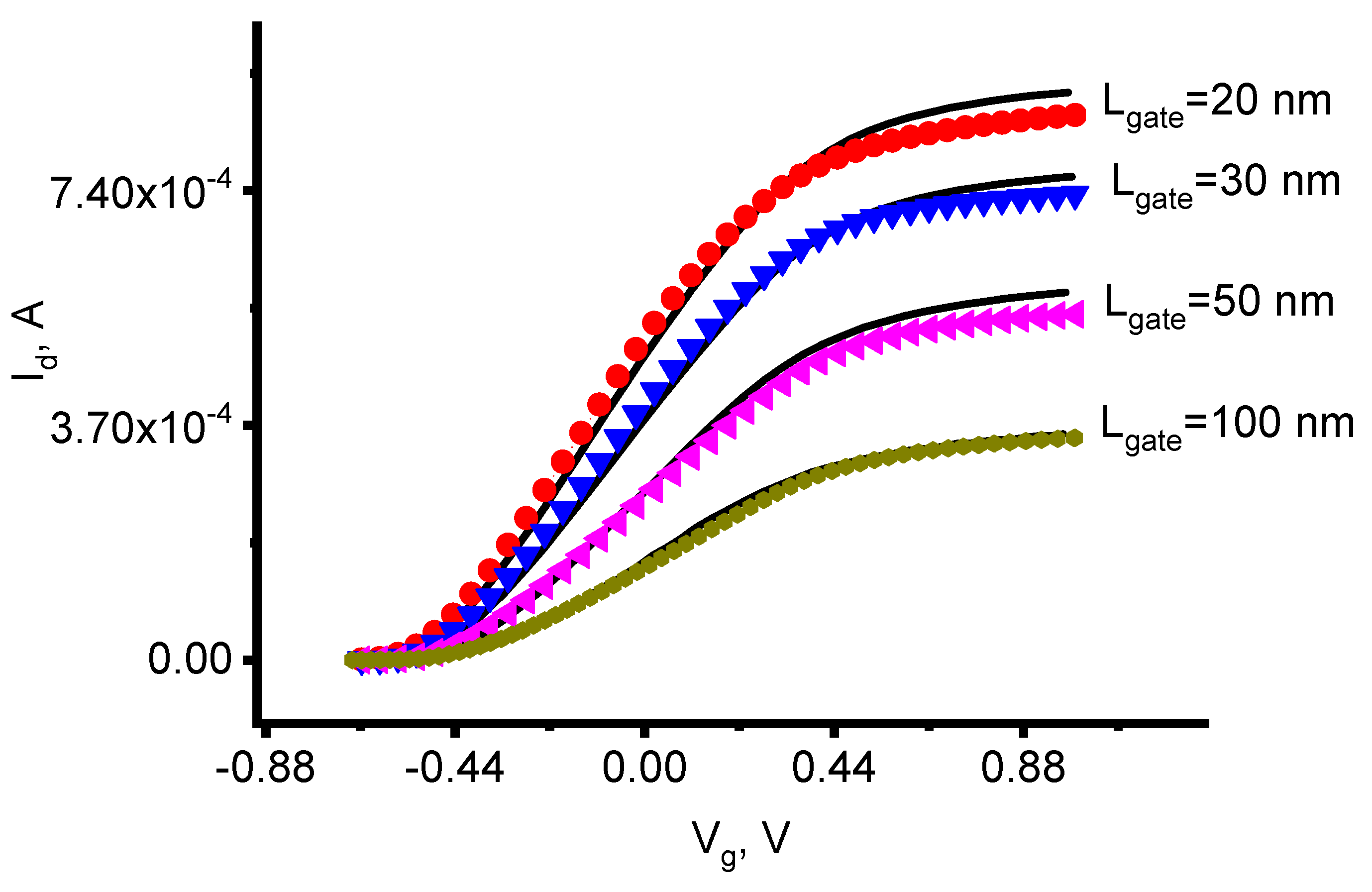
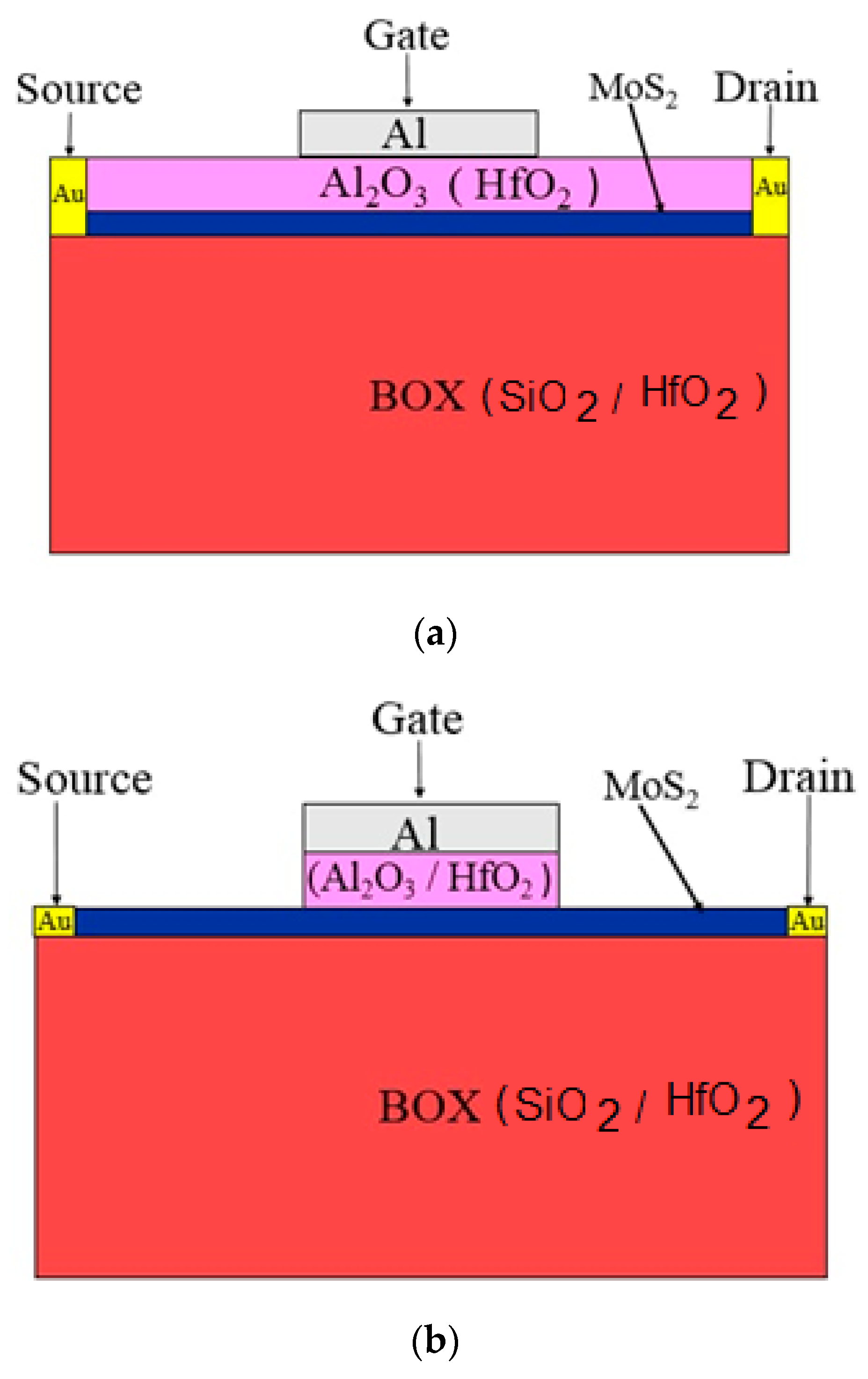
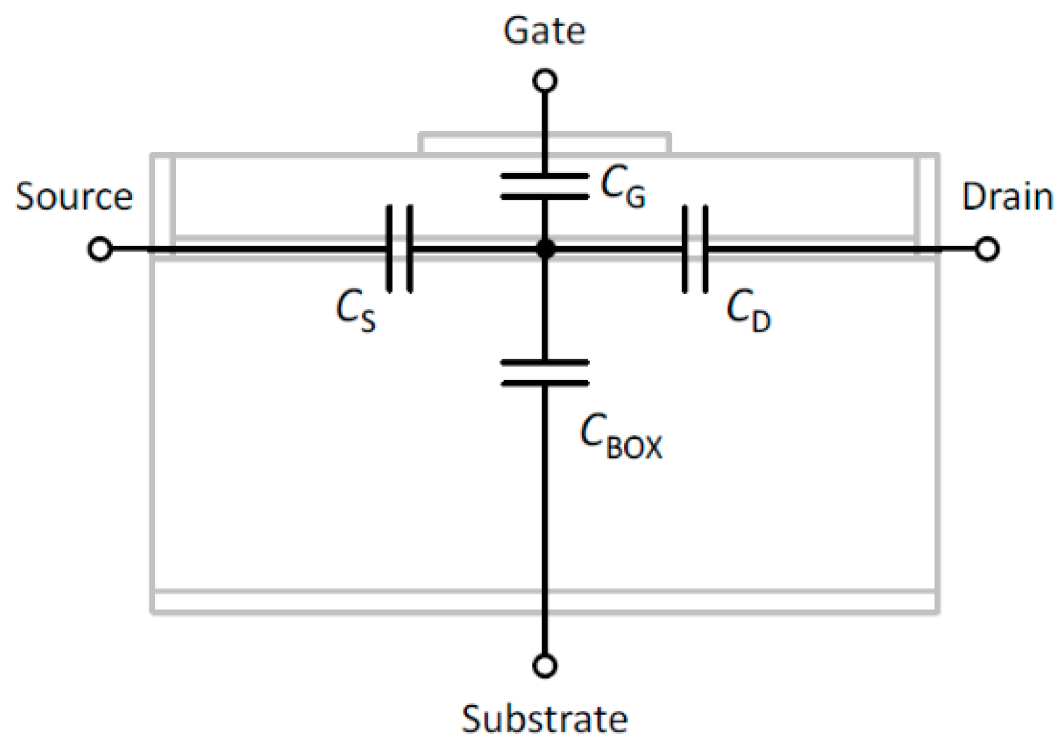
2. Simulation Conditions and Parameterization of the Transistor

The advanced TCAD tool Sentaurus is used to numerically simulate the device. Since 2D MoS2 is not included in the standard version of Sentaurus, the parameters and simulation methods proposed in [2,13] are implemented. The main idea of the method for simulating 2D material-based MOSFETs proposed in [2,13] consists of the following steps: (1) the compilation of data for the material and transport parameters needed for the simulation of 2D material-based MOSFET; (2) the elaboration of a suitable approach to correctly describe the density of states (DOS) and the quantum capacitance in 2D material-based MOS structures; and (3) the implementation of these features in TCAD. It has been shown that carrier transport in 2D MoS2 MOSFETs with channels of dimensions 10 nm and even sub 10 nm are still far from ballistic but dissipative and scattering dominated channels [14,15,16]. The drift–diffusion approach is also considered a reasonable guide in the presence of transient and quasi-ballistic transport in short-channel MOSFETs as it correctly accounts for both device geometry and electrostatics [17]. In order to account for thermal effects, the thermodynamic transport model is used in conjunction with the drift–diffusion transport model in our simulation. To calibrate the model used, simulation results of the Id-Vg characteristics are compared with the results in [2]. The comparison for different gate lengths of the transistor (see Figure 1) has led to a good agreement.
The channel of the simulated transistor consists of a MoS2 monolayer with a thickness of 0.65 nm, and the total length of the device varies between 60 nm and 300 nm depending on the gate length. For all considered transistors, the channel length is three times longer than the gate length. The aluminum gate has a thickness of 2 nm and lengths of 20 nm, 30 nm, 50 nm and 100 nm. The charge carrier mobility in the channel depends on the gate oxide material, so we used a mobility of 125 cm2/(V·s) for Al2O3 [2] and 320 cm2/(V·s) for HfO2 gate oxide (see ref. [18]).
In order to define the optimal structure of the transistor to increase the immunity against degradation effects, the SHE and DIBL effects for a MOSFET with 2D MoS2 as transistor channel are simulated in two cases (see Figure 2). In the first case, the length of the gate oxide is equal to the length of the MoS2 channel (Figure 2a), and in the second case, the length of the gate oxide is equal to the length of the gate (Figure 2b).
The simulation is performed considering the four combinations of gate oxide and back oxide materials (see Table 1). An equivalent gate oxide thickness of 1 nm is chosen for all combinations. Therefore, SiO2-based gate oxide is not considered to likely rule out possible gate leakage current at such thicknesses. Since Al2O3 is practically not used as a back oxide material in MOSFETs, Al2O3 is not considered as a back oxide material in this work. The thickness of the BOX material has a high impact on the temperature of the transistor channel [19]. The temperature in the channel is increased with increasing thickness of the BOX. In our simulation, we have chosen a thickness of BOX 80 nm. This thickness is in the range of BOX thicknesses of the field effect transistors considered in many works, for example in [20] which was devoted to the investigation SHE in hybrid FinFET [20].

3. Simulation Results and Discussion

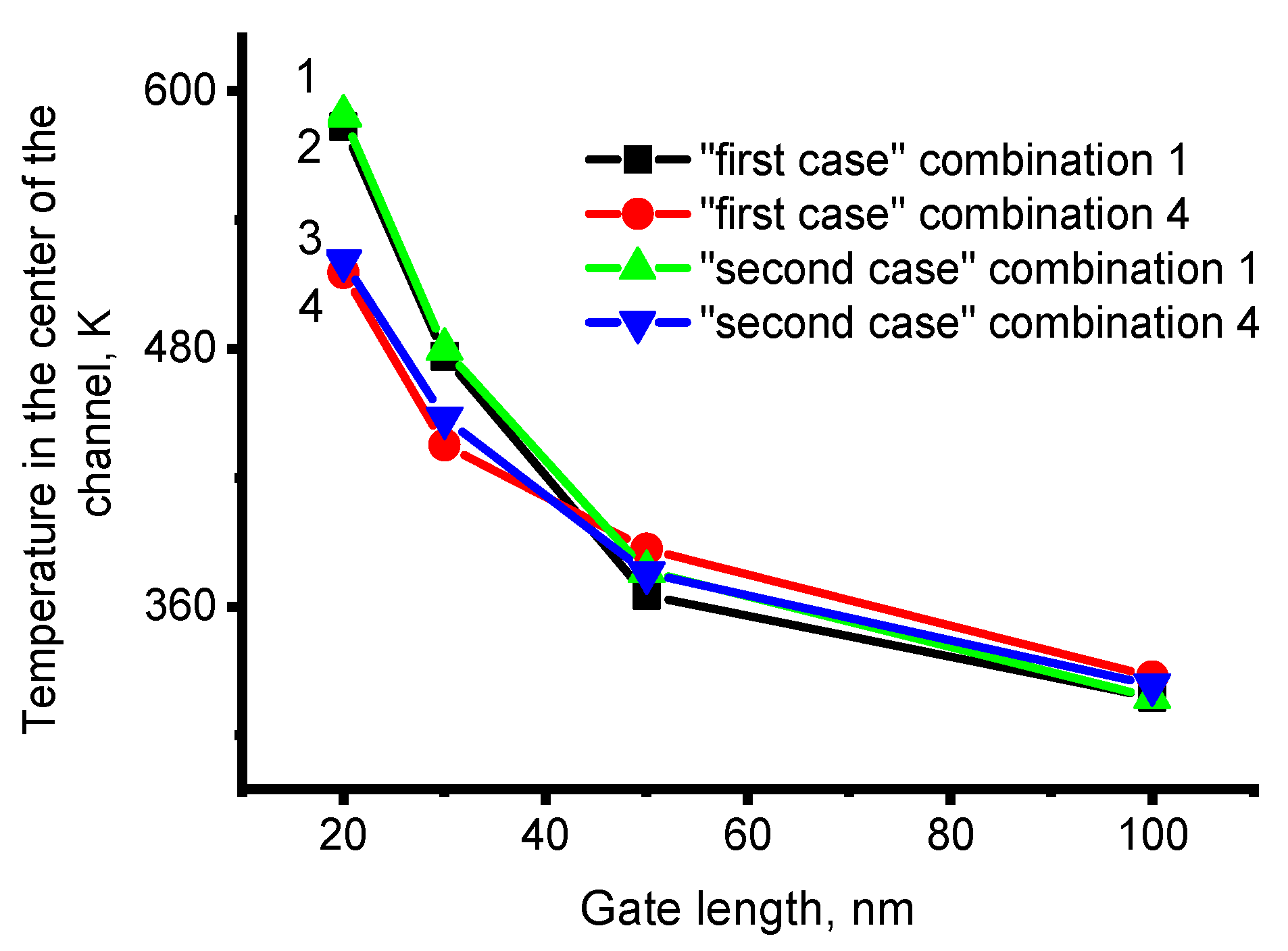
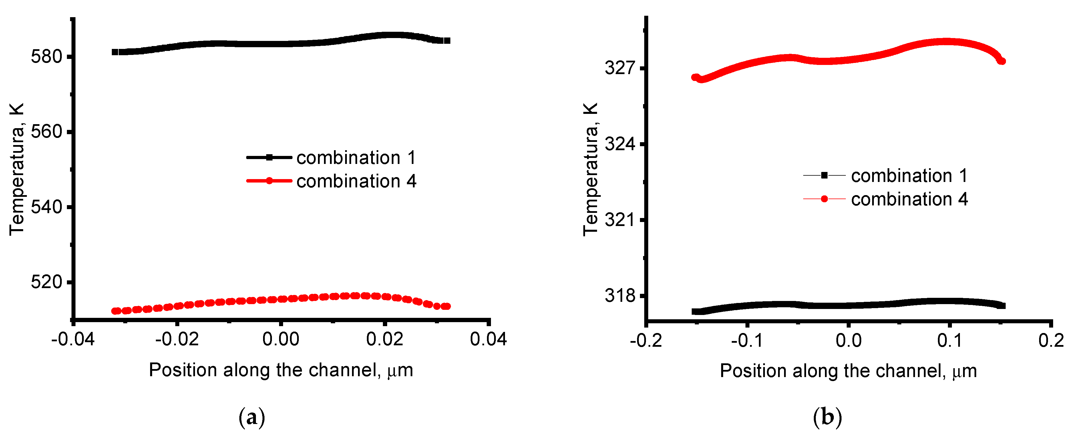
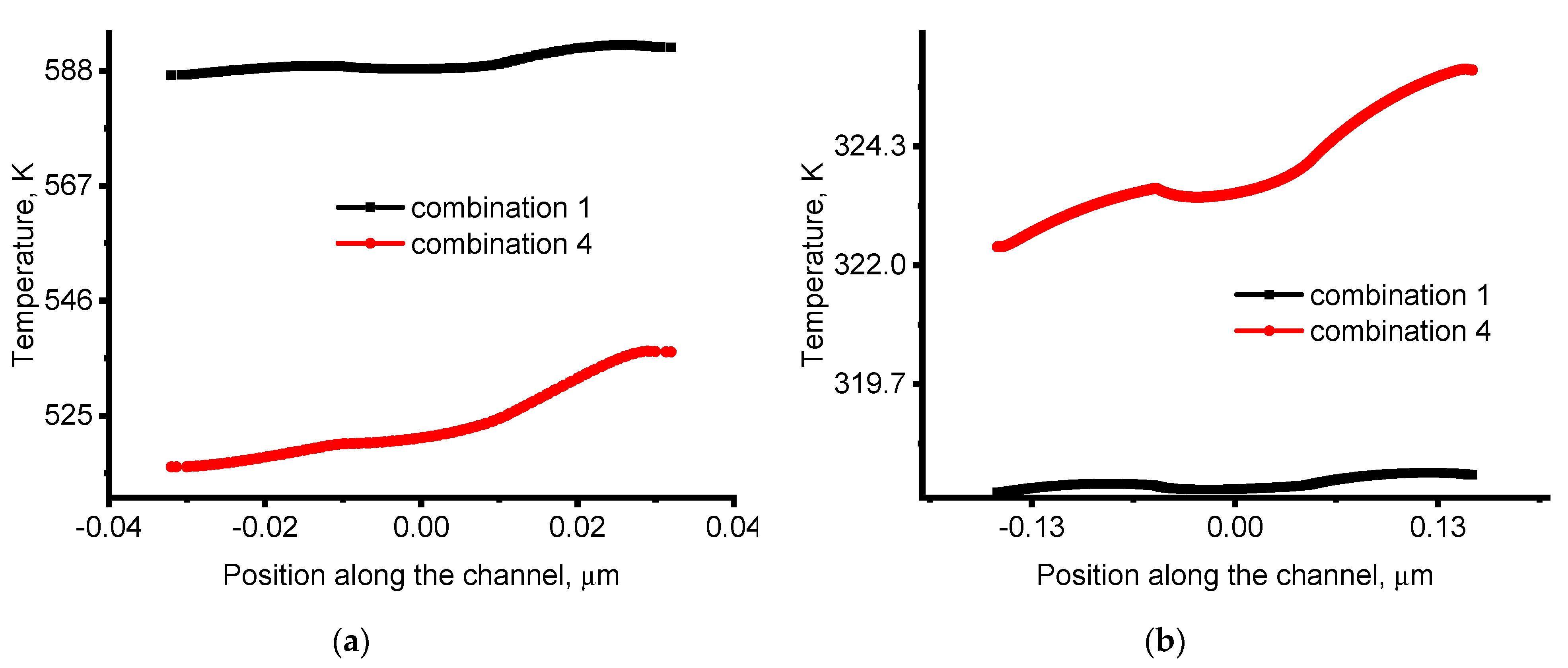
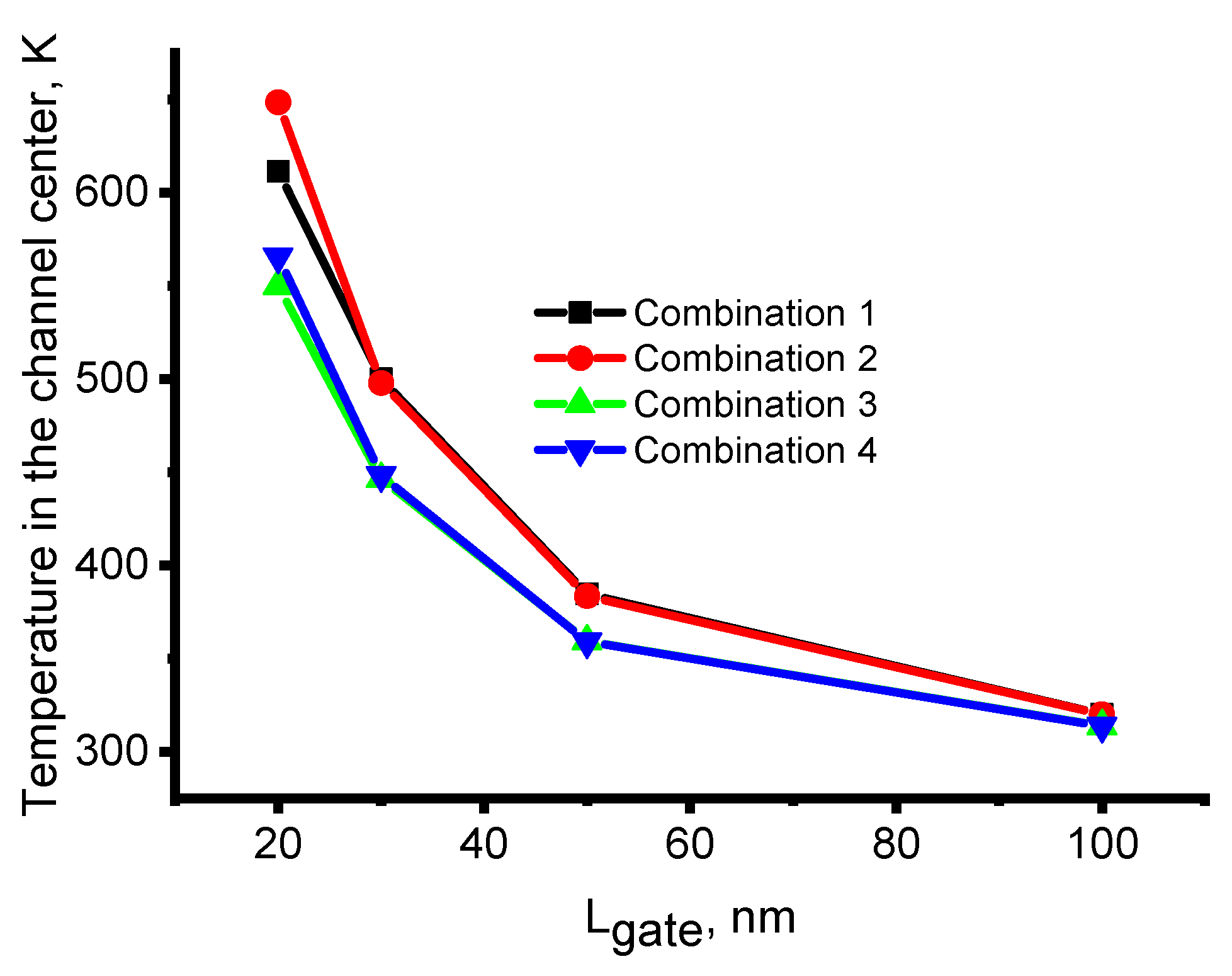
3.1. SHE for Different Combinations of the Gate Oxide and Back Oxide Materials

One of the main parameters of the SHE effect is the temperature in the middle of the channel. The resulting temperature at the center of the channel is defined by the rate of heat generation as well as the rate of heat dissipation through the oxide surrounding the channel. In this study, only heat dissipation is considered, assuming that heat generation is similar in all cases considered. The similar heat generation rate in all the considered cases is provided by choosing the appropriately applied voltages on the gate and drain electrodes. The rate of heat dissipation in the channel is defined by the transistor structure as well as the properties of the oxide materials surrounding the channel. Various considered structures are shown in Figure 2, and various combinations of gate oxide and back oxide materials are shown in Table 1.
The simulation results of the lattice temperature dependence of the gate length at the center of the channel for case 1 (channel surface fully covered) and case 2 (channel surface partially covered) are shown in Figure 3. For all transistors, the temperature distribution along the channel was simulated at fixed (or constant) gate and drain voltages: Vg = 0.1 V and Vd = 0.4 V. As the resistance of long channel transistors is higher, their drain current is lower than the drain current of short channel transistors at the same applied voltages. Higher drain current in short channel transistors results in higher temperature in the middle of the channel compared to the temperature at the center of the channel in the case of long channel transistors. Our different numerical simulations have shown that the temperature at the center of the channel for short channel transistors is higher in both cases (i.e., cases 1 and 2) and for two specific combinations (i.e., combinations 1 and 4). Moreover, although the temperature depends on the length of the channel, it is important to note that it also depends on the structure and the oxide materials. These dependencies are discussed later in this section. The temperature dependence on the applied voltages Vg and Vd was also addressed in our previous work (see ref. [9]).
With a gate length less than 40 nm, for combinations 1 and 4, the lattice temperature in the middle of the channel is slightly higher for transistors where the channel is covered with gate oxide only under the gate (second case) than for the transistors of the first case. This is related to the quite different thermal conductivity of gate oxide materials and air. In the first case, the transistor channel is fully covered with oxide (Figure 2a), while in the second case it is partially covered with air (Figure 2b). In the wide temperature range (between 90 K and 1473 K), the thermal conductivity of air has values between 0.0084 and 0.0915 W/(m K). These values of the thermal conductivity of air (even appropriate for 1473 K) are 2–3 orders of magnitude lower than the thermal conductivity of aluminum- and hafnium-oxides. Thermal conductivities of Al2O3 and HfO2, depending on the size and temperature, are in the ranges of 6–30 W/(m∙K) [21,22,23,24] and 0.27–4.3 W/(m∙K) [25,26], respectively.
The effect of the thermal expansion of the channel is not taken into account in this simulation, because the coefficient of thermal expansion is too low (i.e., very small). According to [27], the coefficient of thermal expansion of the MoS2 monolayer at 550 K is 6.5∙10−3 1/K, which means a channel expansion of only 1.95% at a change in the temperature of 300 K.
For transistors with a channel length greater than 40 nm, the mid-channel temperature for the transistors of the first case became higher than for the transistors of the second case (Figure 3). This means that the impact of oxide materials on the establishment of the resulting temperature at the center of the channel becomes greater than the impact of the transistor structure (cases 1 and 2) for long channel transistors. In other words, for long-channel transistors, heat dissipation through oxides is much greater than in short-channel transistors, and heat dissipation through gas has no decisive role (i.e., is not so important) in establishing the resulting temperature in the channel.
For long-channel transistors, the temperature tends to be the same for all types of transistor structures considered. In this case, it is observed that the heat generation rate plays a more sufficient role than the heat dissipation rate, since the resulting temperature is the same for both structures (case 1 and case 2) and for both combinations 1 and 4. From the temperature distribution along the channel for case 1 (fully covered channel top) and case 2 (partially covered channel top), it can be seen that with the same applied gate and drain voltages, the temperature variation when lengthening the gate, for the transistor with combination 1 is higher than for the transistor with combination 4 (Table 1) (Figure 4 and Figure 5). The change in center channel temperature is 264 K and 192 K in case 1, 270 K and 194 K in case 2 for combinations 1 and 4, respectively. Apparently this is mainly related to the higher thermal conductivity of Al2O3 compared to the thermal conductivity of HfO2 (Table 2), which is used as gate oxide materials in combinations 1 and 4, respectively. Although the thermal conductivity of SiO2 used as BOX material in combination 1 is lower than the thermal conductivity of HfO2 used as BOX material in combination 4, it differs only by 1.5 times, while the thermal conductivity of gate oxide materials is about 5 times different (Table 2).
The simulation results for a wider range of oxide material combinations show that SHE is gate length-sensitive for all combinations of gate and back oxide materials in the transistor (Figure 6). The SHE dependence on gate length has only been shown for transistors of case 1, since this dependence is the same for transistors of case 2. The sensitivity of SHE to gate length can be explained by the dependence of drain current on channel length, which in our analysis is based on gate length. Therefore, since the drain current defines the heat generation rate, a long channel (small drain current) reduces the heat generation rate. The reduction in temperature for long channel transistors and its convergence to the same value for all four oxide material combinations supports our assumption that for long channels the main mechanism responsible for the formation of the resulting temperature is the heat generation rate.
The temperature dynamics (or behavior) shown in Figure 6 can be explained by the heat dissipation through the gate oxide and BOX. It is known that “low thermal conductivity of oxide materials” results in slower heat dissipation from the material and formation of a higher equilibrium channel temperature than in “higher thermal conductivity of oxide materials”. Therefore, the thermal conductivity of the gate oxide and BOX materials is a very important parameter in SHE. Depending on the thickness, the thermal conductivity of HfO2 films has values in the range of 0.27–4.3 W/(m·K) at temperatures between 300 °C and 500 °C [26,28]. The values of the thermal conductivity of SiO2 are in the range between 0.5 W/(m·K) and 2.5 W/(m·K) [29,30]. In our simulation, we used the thermal conductivity values shown in Table 2. We chose the thermal conductivities for HfO2 and SiO2 as average values from the indicated above ranges. Thermal conductivity for Al2O3 considerably depends on the thickness and the temperature. It is varied in the range between 6 and 30 W/(m∙K) [21,22,23,24] as mentioned above, in Section 3.1. The value 12 W/(m∙K) was chosen as the value corresponding to the nanoscale (less than 10 nm) oxide layer and for a temperature range of approximately between 100 and 300 °C.
With gate lengths up to 100 nm, the mid-channel temperature is higher for transistors with combinations 1 and 2 than for transistors with combinations 3 and 4. Apparently, this is mainly related to a lower thermal conductivity of the BOX material in combinations 1 and 2 (which is SiO2) than the thermal conductivity of the BOX material in combinations 3 and 4 (which is HfO2). With the smallest gate length (e.g., a length of less than 30 nm) for combinations with the same BOX material, the temperature is higher for combinations with HfO2 as the gate oxide material. With gate lengths between 30 nm and 100 nm, the temperature for combinations with the same BOX material is approximately the same and practically independent of the gate oxide material. With a gate length of 100 nm, the temperature is practically the same for all four combinations, which means that with long gate lengths, the resulting center channel temperature does not depend on the gate oxide and BOX materials.

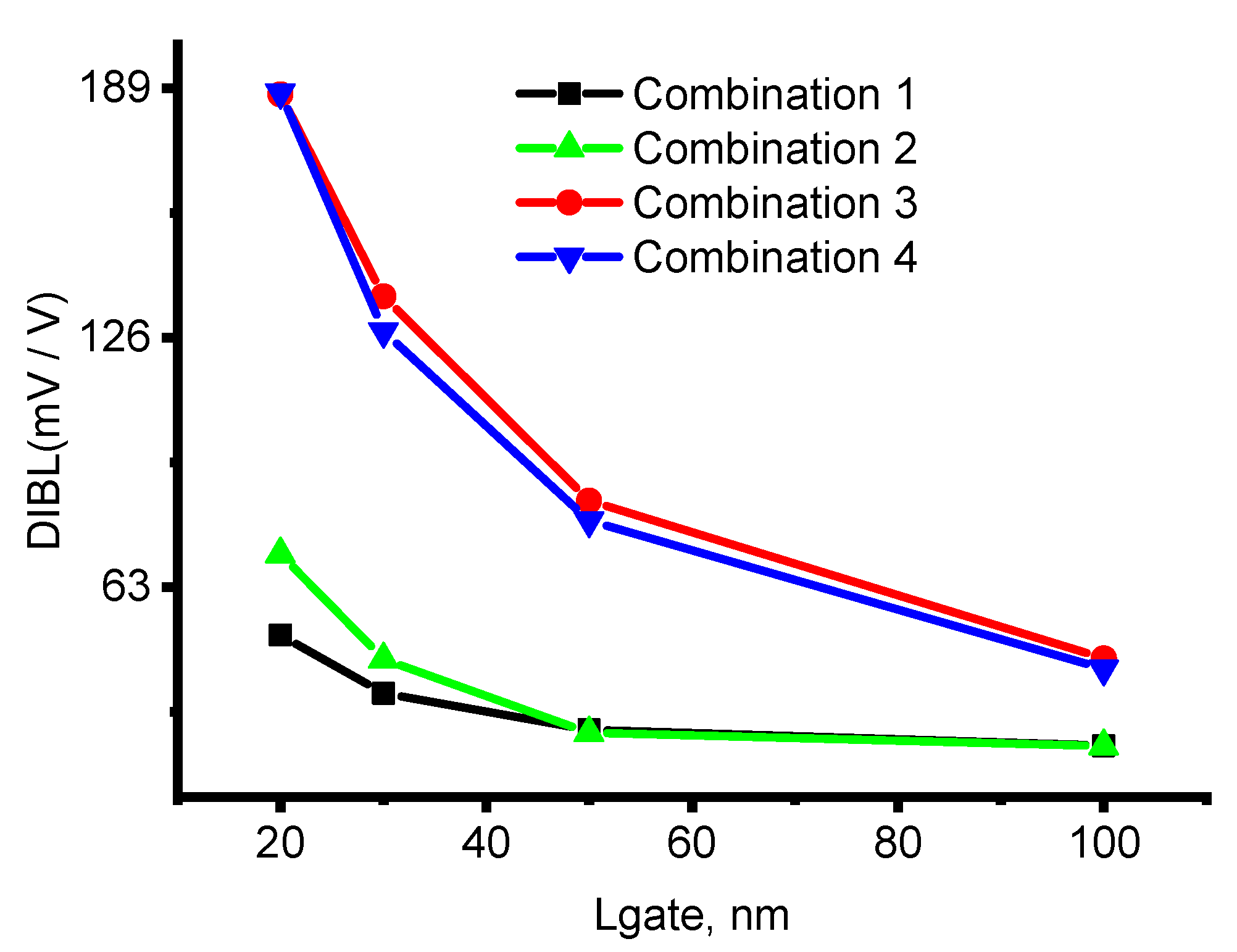
3.2. DIBL Effect for Different Combinations of the Gate Oxide and Back Oxide Materials

The DIBL effect is one of the SHE-like degradation effects which also depends on the properties of the gate oxide and BOX materials. For comparison with the SHE effect, the DIBL effect was simulated in a MOSFET with 2D MoS2 as transistor channel with the four combinations of gate oxide and BOX materials mentioned above. The simulation results show that the DIBL effect for transistors with combinations 3 and 4 is more sensitive to gate length (Figure 7). In all ranges of transistor length, the DIBL effect is higher for transistors with combinations 3 and 4 than for transistors with combinations 1 and 2. This observation can be understood in the context of a simple model describing the capacitive coupling between the channel and the device electrodes, proposed in [12]. Within the context of a simple model, the modified expression for DIBL is expressed as follows [12]:
D I B L = C D C G
where, CD and CG are drain-channel and gate-channel capacitances, respectively (Figure 8). Three components contribute to the drain-channel capacitance (CD): the capacitive coupling through the channel layer (CD.ch), the coupling through the BOX (CDbox), and the coupling through the gate oxide (CD.ox). Therefore, the drain-channel capacitance (CD) is expressed as follows:
C D = C D . c h + C D b o x + C D . o x  
The capacitance components CG, CD.ch, and CD.ox depend on the dielectric constant of the channel εMoS2, while CD.box is unaffected by  ε M o S 2  and depends on the dielectric constant of the BOX material. In our case,  ε A l 2 O 3 = 9.3 ε S i O 2 = 3.9  and  ε H f O 2 = 25  and  ε M o S 2 = 3 . Therefore, since the dielectric constant of the channel  ε M o S 2  is smaller, the gate capacitance CG and the components CD.ch and CD.ox are reduced, and the DIBL effect is mainly defined by CD.box. Thus, for the considered transistors, the DIBL effect is defined by the dielectric constant of the BOX. In the range of combinations, the BOXs with the highest dielectric constant are in combinations 3 and 4, where oxide materials are HfO2 with  ε H f O 2 = 25 , hence these combinations should show the highest DIBL effects. Therefore, while the BOX material for the transistors with combinations 1 and 2 is SiO2 with a lower dielectric constant ( ε S i O 2 = 3.9 ), the DIBL effect for these transistors should be low. These suggestions are in perfect agreement with Figure 7. It can also be seen in Figure 7 that the gate oxide material does not have a considerable impact (or influence) on the DIBL effect in the considered range of variation of the gate length.

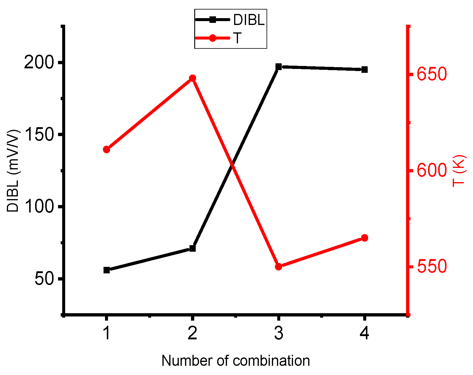
3.3. Optimization of the Combination of the Gate Oxide and Back Oxide Materials

The dependence of lattice temperature and DIBL on the number of combinations that can be seen from Figure 6 and Figure 7 for a gate length of 20 nm is shown in Figure 9. It is clear from Figure 9 that the SHE and DIBL effects compete for the combination of the oxide materials. As already discussed above, the electrical and thermal properties of the back oxide material, namely dielectric constant and thermal conductivity, are mainly responsible for the SHE and DIBL effect in the considered 2D MoS2 MOSFETs.
Achieving a small DIBL effect requires a low dielectric constant back oxide material, while reducing the gate temperature in the transistor channel requires a high thermal conductivity back oxide material. We have considered two popular and commonly used back oxide materials: SiO2 and HfO2. When the back oxide material is SiO2, it has a small dielectric constant, resulting in a decrease in DIBL; at the same time, it also has low thermal conductivity, which leads to high lattice temperature in the transistor channel. Conversely, as a back oxide material, HfO2 material has a high dielectric constant, resulting in a high DIBL effect, while also exhibiting a relatively high thermal conductivity, resulting in a reduction in the lattice temperature in the transistor channel.
From our results, it is possible to define the range of electrical and thermal parameters of oxide materials that allow to achieve optimal immunity to SHE as well as the DIBL effect. From Figure 7, it can be concluded that using the BOX material with a relative dielectric constant in the range between 3.9 and 25 and a thermal conductivity between 1.4 and 2.3 W/Km is a perfect choice to achieve (or for achieving) optimal immunity to degradation effects, such as SHE and DIBL effects in 2D MoS2-based MOSFETs. The gate oxide material has practically no significant influence on SHE as well as on the DIBL effect.

4. Conclusions

The results of the simulation of the SHE effect have revealed that with a gate length of less than 40 nm, a greater influence on the resulting temperature was exerted on the considered structures of the transistor (see case 1 and case 2) than the influence of the gate oxide and the BOX materials. Furthermore, it was observed that SHE is sensitive to gate length for all combinations of gate and back oxide materials in the transistor, while the DIBL effect is more sensitive to gate length for transistors with combinations 3 and 4.
Moreover, our simulation results revealed that the choice of gate and BOX oxide materials to ensure the highest possible immunity against degradation effects, such as SHE and DIBL effects, is an optimization task in 2D MoS2-based MOSFETs. The electrical and thermal properties of the back oxide material have been shown to have a major influence on the SHE and DIBL effects in 2D MoS2-based MOSFETs. Indeed, the use of the BOX material with a relative dielectric constant between 3.9 and 25 and a thermal conductivity between 1.4 and 2.3 W/(K∙m) makes it possible to obtain optimum immunity against degradation effects, such as SHE and DIBL effects, in 2D MoS2-based MOSFETs. Finally, it was observed that the gate oxide material has almost no considerable impact on the SHE effect as well as the DIBL effect.

Author Contributions

Conceptualization, A.E.A.; methodology, A.E.A. and A.Y.; software, K.S.S.; validation, A.E.A. and K.S.S.; formal analysis, J.C.C. and A.Y; investigation, K.S.S.; resources, K.S.S.; data curation, K.S.S.; writing—original draft preparation, A.E.A.; writing—review and editing, A.E.A. and J.C.C.; visualization, J.C.C. and A.Y.; supervision, A.E.A.; project administration A.E.A.; funding acquisition, A.E.A. All authors have read and agreed to the published version of the manuscript.

Funding

This research was funded by the Ministry of Innovation Development of the Republic of Uzbekistan, grant number Ind-Uzb-2021-80.

Institutional Review Board Statement

Not applicable.

Informed Consent Statement

Not applicable.

Data Availability Statement

Data is unavailable due to privacy.

Conflicts of Interest

The authors declare no conflict of interest.

Abbreviations

SHESelf-Heating Effect
DIBLDrain-Induced Barrier Lowering
MOSFETMetal-Oxide-Semiconductor Field Effect Transistor
BOXBack oxide
TMDTransition Metal Dichalcogenide
CMOSComplementary Metal-Oxide-Semiconductor
DOSDensity of States
2DTwo Dimensional
TCADTechnology Computer Aided Design

References

  1. Radisavljevic, B.; Radenovic, A.; Brivio, J.; Giacometti, V.; Kis, A. Single-Layer MoS2 Transistors. Nat. Nanotechnol. 2011, 6, 147–150. [Google Scholar] [CrossRef]
  2. Geng, Z. Simulation of Graphen Nanoribbon and MoS2 Transistors. Master’s Thesis, TU Ilmenau, Ilmenau, Germany, 2016; pp. 3–17. (In German). [Google Scholar]
  3. Liu, H.; Neal, A.T.; Ye, P.D. Channel Length Scaling of MoS2 MOSFETs. ACS Nano 2012, 6, 8563–8569. [Google Scholar] [CrossRef]
  4. Tong, X.; Ashalley, E.; Lin, F.; Li, H.; Wang, Z.M. Advances in MoS2-Based Field Effect Transistors (FETs). Nano-Micro Lett. 2015, 7, 203–218. [Google Scholar] [CrossRef] [PubMed]
  5. Guo, Y.; Wei, X.; Shu, J.; Liu, B.; Yin, J.; Guan, C.; Han, Y.; Gao, S.; Chen, Q. Charge trapping at the MoS2-SiO2 interface and its effects on the characteristics of MoS2 metal-oxide-semiconductor field effect transistors. Appl. Phys. Lett. 2015, 106, 103109. [Google Scholar] [CrossRef]
  6. Atamuratov, A.E.; Jabbarova, B.O.; Khalilloev, M.M.; Sivasankaran, K.; Chedjou, J.C. Impact of the channel shape, back oxide and gate oxide layers on self-heating in nanoscale JL FINFET. Nanosyst. Phys. Chem. Math. 2022, 13, 148–155. [Google Scholar] [CrossRef]
  7. Atamuratov, A.E.; Jabbarova, B.O.; Khalilloev, M.M.; Yusupov, A. The Self-Heating Effect in Junctionless Fin Field-Effect Transistors Based on Silicon-on-Insulator Structures with Different Channel Shapes. Tech. Phys. Lett. 2021, 47, 542–545. [Google Scholar] [CrossRef]
  8. Atamuratov, A.E.; Jabbarova, B.O.; Khalilloev, M.M.; Yusupov, A.; Loureiro, A.G. Self-heating effect in nanoscale SOI Junctionless FinFET with different geometries. In Proceedings of the 2021 13th Spanish Conference on Electron Devices (CDE), Sevilla, Spain, 9–11 June 2021; pp. 62–65. [Google Scholar]
  9. Atamuratov, A.E.; Saparov, X.S.; Atamuratov, T.; Yusupov, A.; Schwierz, F. The contribution of gate and drain voltages to temperature distribution along the channel in 2D MoS2 based MOSFET. In Proceedings of the 2021 International Conference on Information Science and Communications Technologies (ICISCT), Tashkent, Uzbekistan, 3–5 November 2021; pp. 1–3. [Google Scholar] [CrossRef]
  10. Tiwari, S.; Dolai, S.; Rahaman, H.; Gupta, P.S. Effect of temperature & phonon scattering on the drain current of a MOSFET using SL-MoS2 as its channel material. Superlattices Microstruct. 2017, 111, 912–921. [Google Scholar] [CrossRef]
  11. Wolf, S. The Submicron MOSFET, Vol. 3 of Silicon Processing for the VLSI Era; Lattice Press: Sunset Beach, CA, USA, 1995. [Google Scholar]
  12. Granzner, R.; Geng, Z.; Kinberger, W.; Schwierz, F. MOSFET scaling: Impact of two-dimensional channel materials. In Proceedings of the 2016 13th IEEE International Conference on Solid-State and Integrated Circuit Technology (ICSICT), Hangzhou, China, 25–28 October 2016; pp. 466–469. [Google Scholar] [CrossRef]
  13. Bondja, C.N.; Geng, Z.; Granzner, R.; Pezoldt, J.; Schwierz, F. Simulation of 50-nm Gate Graphene Nanoribbon Transistors. Electronics 2016, 5, 3. [Google Scholar] [CrossRef]
  14. Szabo, A.; Rhyner, R.; Luisier, M. Ab-initio simulations of MoS2 transistors: From mobility calculation to device performance evaluation. In Proceedings of the 2014 IEEE International Electron Devices Meeting (IEDM), San Francisco, CA, USA, 15–17 December 2014; pp. 725–728. [Google Scholar] [CrossRef]
  15. Cao, W.; Kang, J.; Sarkar, D.; Liu, W.; Banerjee, K. Performance evaluation and design considerations of 2D semiconductor based FETs for sub-10 nm VLS. In Proceedings of the 2014 IEEE International Electron Devices Meeting (IEDM), San Francisco, CA, USA, 15–17 December 2014; pp. 729–732. [Google Scholar]
  16. Liu, L.; Lu, Y.; Guo, J. On Monolayer MoS2 Field-Effect Transistors at the Scaling Limit. IEEE Trans. Electron Devices 2013, 60, 4133–4139. [Google Scholar] [CrossRef]
  17. Ancona, M.G. Electron Transport in Graphene From a Diffusion-Drift Perspective. IEEE Trans. Electron Devices 2010, 57, 681–689. [Google Scholar] [CrossRef]
  18. Bharathi, N.D.; Sivasankaran, K. Influence of metal contact on the performance enhancement of monolayer MoS2 transistor. Superlattices Microstruct. 2018, 120, 479–486. [Google Scholar] [CrossRef]
  19. McDaid, L.; Hall, S.; Mellor, P.; Eccleston, W.; Alderman, J. Physical origin of negative differential resistance in SOI transistors. Electron. Lett. 1989, 25, 827–828. [Google Scholar] [CrossRef]
  20. Nelapati, R.P.; Sivasankaran, K. Impact of self-heating effect on the performance of hybrid FinFET. Microelectron. J. 2018, 76, 63–68. [Google Scholar] [CrossRef]
  21. Dongre, B.; Carrete, J.; Mingo, N.; Madsen, G.K.H. Ab initio lattice thermal conductivity of bulk and thin-film α-AI2O3. MRS Commun. 2018, 8, 1119–1123. [Google Scholar] [CrossRef]
  22. Galusek, D.; Galusková, D. Alumina Matrix Composites with Non-Oxide Nanoparticle Addition and Enhanced Functionalities. Nanomaterials 2015, 5, 115–143. [Google Scholar] [CrossRef]
  23. Kita, J.; Engelbrecht, A.; Schubert, F.; Groß, A.; Rettig, F.; Moos, R. Some practical points to consider with respect to thermal conductivity and electrical resistivity of ceramic substrates for high-temperature gas sensors. Sens. Actuators B Chem. 2015, 213, 541–546. [Google Scholar] [CrossRef]
  24. Frano, R.L.; Aquaro, D.; Scaletti, L.; Olivi, N. Characterization of the thermal conductivity for ceramic pebble beds. J. Phys. Conf. Ser. 2015, 655, 012057. [Google Scholar] [CrossRef]
  25. Hinz, M.; Marti, O.; Gotsmann, B.; Lantz, M.A.; Dürig, U. High resolution vacuum scanning thermal microscopy of HfO2 and SiO2. Appl. Phys. Lett. 2008, 92, 043122. [Google Scholar] [CrossRef]
  26. Panzer, M.A.; Shandalov, M.; Rowlette, J.A.; Oshima, Y.; Chen, Y.W.; McIntyre, P.C.; Goodson, K.E. Thermal Properties of Ultrathin Hafnium Oxide Gate Dielectric Films. IEEE Electron. Device Lett. 2009, 30, 1269–1271. [Google Scholar] [CrossRef]
  27. Yang, Y.; Lin, Z.; Li, R.; Li, Y.; Liu, W.; Tian, S.; Zhu, K.; Long, L. Thermal expansion coefficient of monolayer MoS2 determined using temperature-dependent Raman spectroscopy combined with finite element simulations. Microstructures 2021, 1, 2021002. [Google Scholar] [CrossRef]
  28. Stolz, C.; Genin, F.; Reitter, T.; Molau, N.; Bevis, R.; Gunten, M.; Smith, D.; Anzellotti, J. Effect of SiO2 overcoat thickness on laser damage morphology of HfO2 ISiO2 Brewster’s angle polarizers at 1064 nm. Proc. SPIE 1997, 2966, 265. [Google Scholar]
  29. Kato, R.; Hatta, I. Termal Conductivity Measurement of Termally-Oxidized SiO2 Films on a Silicon Wafer Using a TermoRefectance Technique. Int. J. Termophysics 2005, 26, 179–190. [Google Scholar] [CrossRef]
  30. Ryningen, B.; Bellmann, M.; Kvande, R.; Lohne, O. The Effect of Crucible Coating and the Temperature Field on Minority Carrier Lifetime in Directionally Solidified Multicrystalline Silicon Ingots. In Proceedings of the 27th European Photovoltaic Solar Energy Conference and Exhibition, Frankfurt, Germany, 24–28 September 2012; pp. 926–932. [Google Scholar] [CrossRef]
Figure 1. Ig-Vd characteristics of the considered 2D MoS2-based MOSFETs with different gate lengths. The gate oxide material is Al2O3 and the BOX material is SiO2 with a thickness of 1020 nm. The drain voltage is Vd = 1 V. Solid lines correspond to the results in [2], and colored markings are the results of our simulation.
Applsci 13 06131 g001
Figure 2. Structure of the simulated MoS2 MOSFET. Two cases are considered: (a) the gate oxide length is equal to the MoS2 channel length (first case); (b) the gate oxide length is equal to the gate length (second case).
Applsci 13 06131 g002
Figure 3. Dependence of lattice temperature at channel center on gate length for 2D MoS2 MOSFETs with Al2O3 gate oxide (1, 2) and HfO2 gate oxide (3, 4) with fully covered channel (2, 4) and with partially covered channel (only under the gate) (1, 3).
Applsci 13 06131 g003
Figure 4. Temperature distribution along the channel for “case 1” transistors with gate oxide materials Al2O3 and HfO2, while BOX material is SiO2 and HfO2, respectively. The gate lengths are 20 nm (a) and 100 nm (b). Vg = 0.1 V, and Vd = 0.4 V.
Applsci 13 06131 g004
Figure 5. Temperature distribution along the channel for “case 2” transistors with gate oxide materials Al2O3 and HfO2, while BOX material is SiO2 and HfO2, respectively. The gate lengths are 20 nm (a) and 100 nm (b). Vg = 0.1 V, and Vd = 0.4 V.
Applsci 13 06131 g005
Figure 6. SHE dependence on the gate length for different combinations of gate oxide and back oxide materials.
Applsci 13 06131 g006
Figure 7. DIBL effect dependence on the gate length for different combinations of gate oxide and back oxide materials.
Applsci 13 06131 g007
Figure 8. Equivalent circuit describing the capacitive coupling between the channel and the device electrodes in MOSFET.
Applsci 13 06131 g008
Figure 9. DIBL effect and SHE dependence of combinations of gate oxide and back oxide materials in MOSFET.
Applsci 13 06131 g009
Table 1. Combination of the gate and back oxide materials considered in the work.
Number of CombinationGate Oxide MaterialBack Oxide Material
1Al2O3SiO2
2HfO2SiO2
3Al2O3HfO2
4HfO2HfO2
Table 2. Thermal conductivities used for simulation.
MaterialThickness
(nm)
Thermal Conductivity
  W K · m
SiO2801.4
Al2O32.38512
HfO2 (gate oxide)5.6412.3
HfO2 (Box)802.3
Disclaimer/Publisher’s Note: The statements, opinions and data contained in all publications are solely those of the individual author(s) and contributor(s) and not of MDPI and/or the editor(s). MDPI and/or the editor(s) disclaim responsibility for any injury to people or property resulting from any ideas, methods, instructions or products referred to in the content.

