
Superconducting Electronic–Photonic Platform for HEB-Based Terahertz Spectrometers
 ,
,
Abstract
:1. Introduction
2. Materials and Methods
3. Results and Discussion
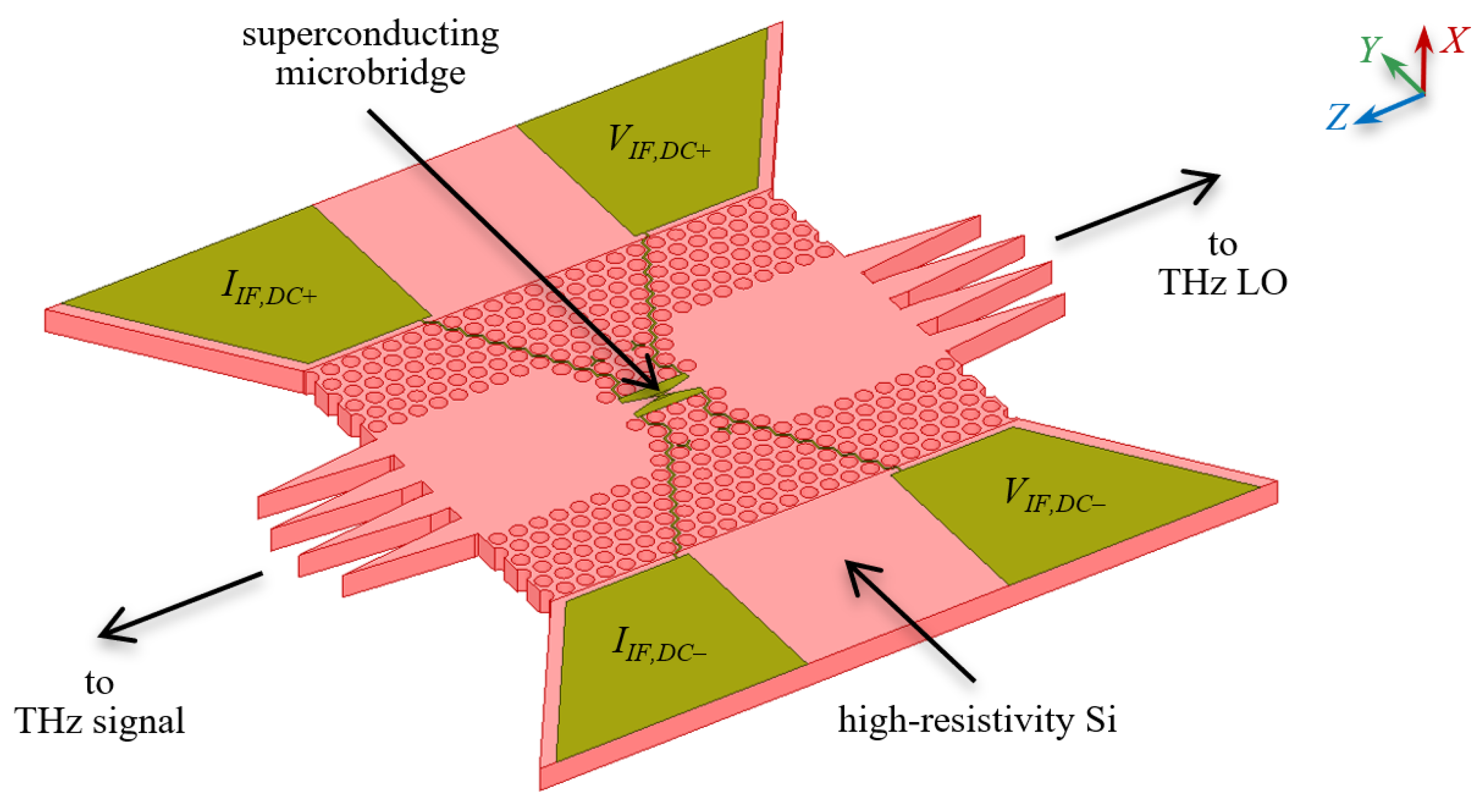
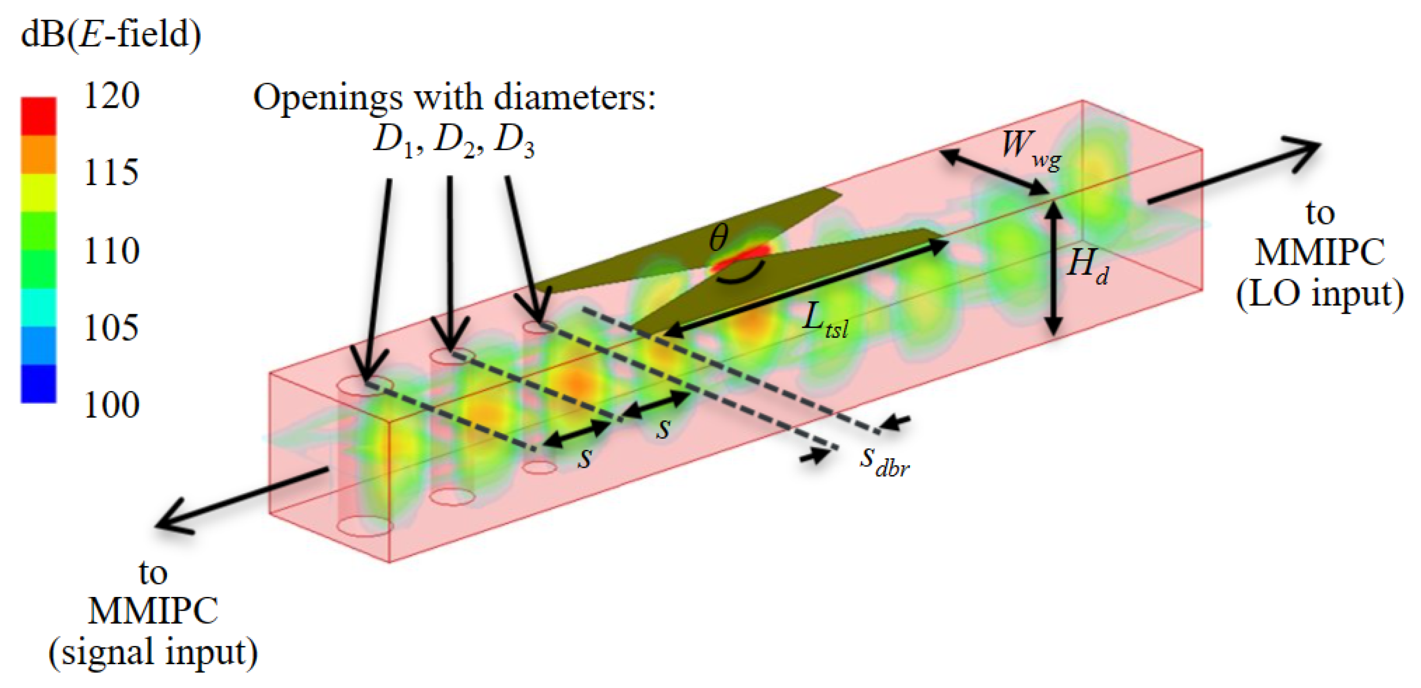
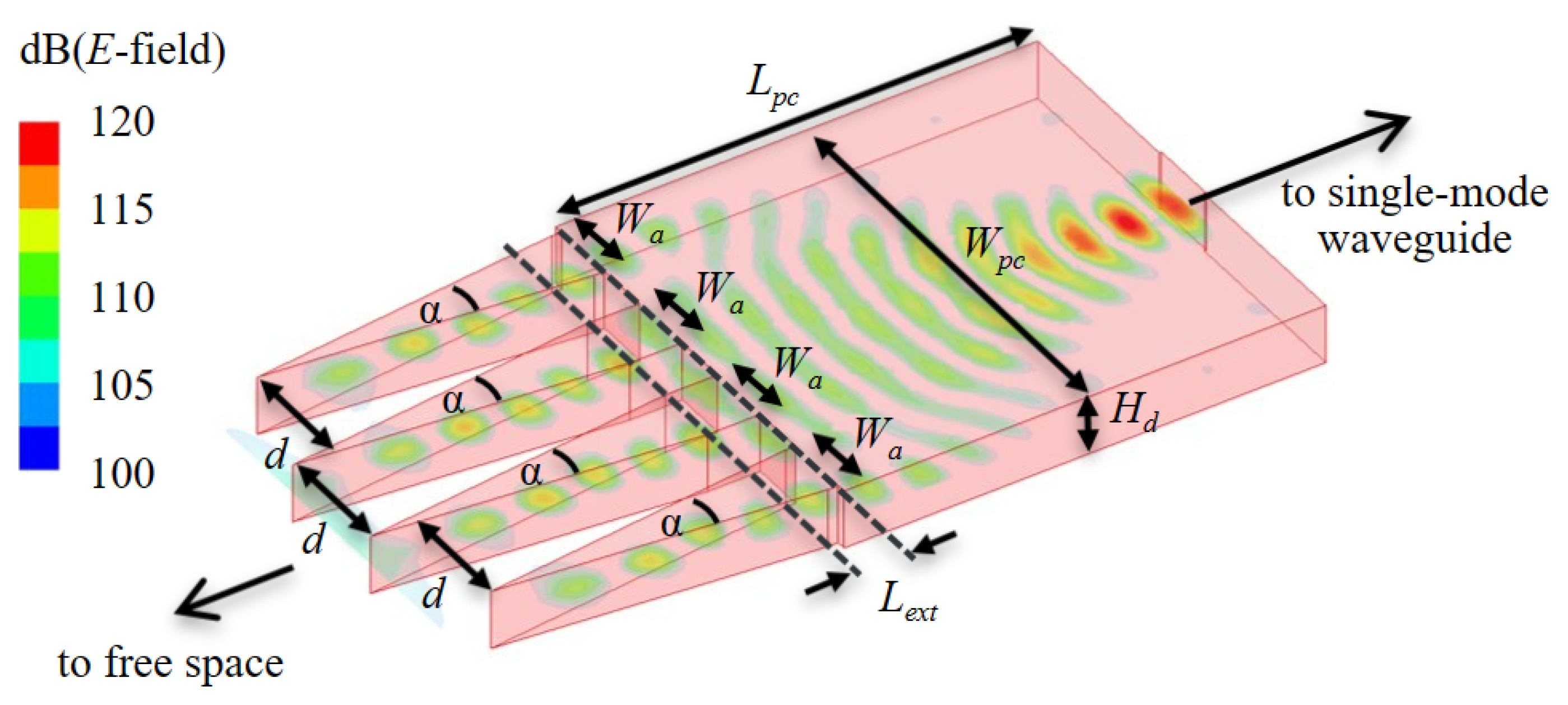
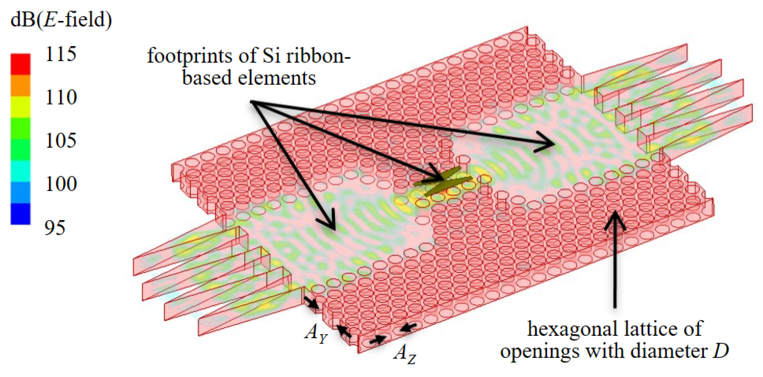
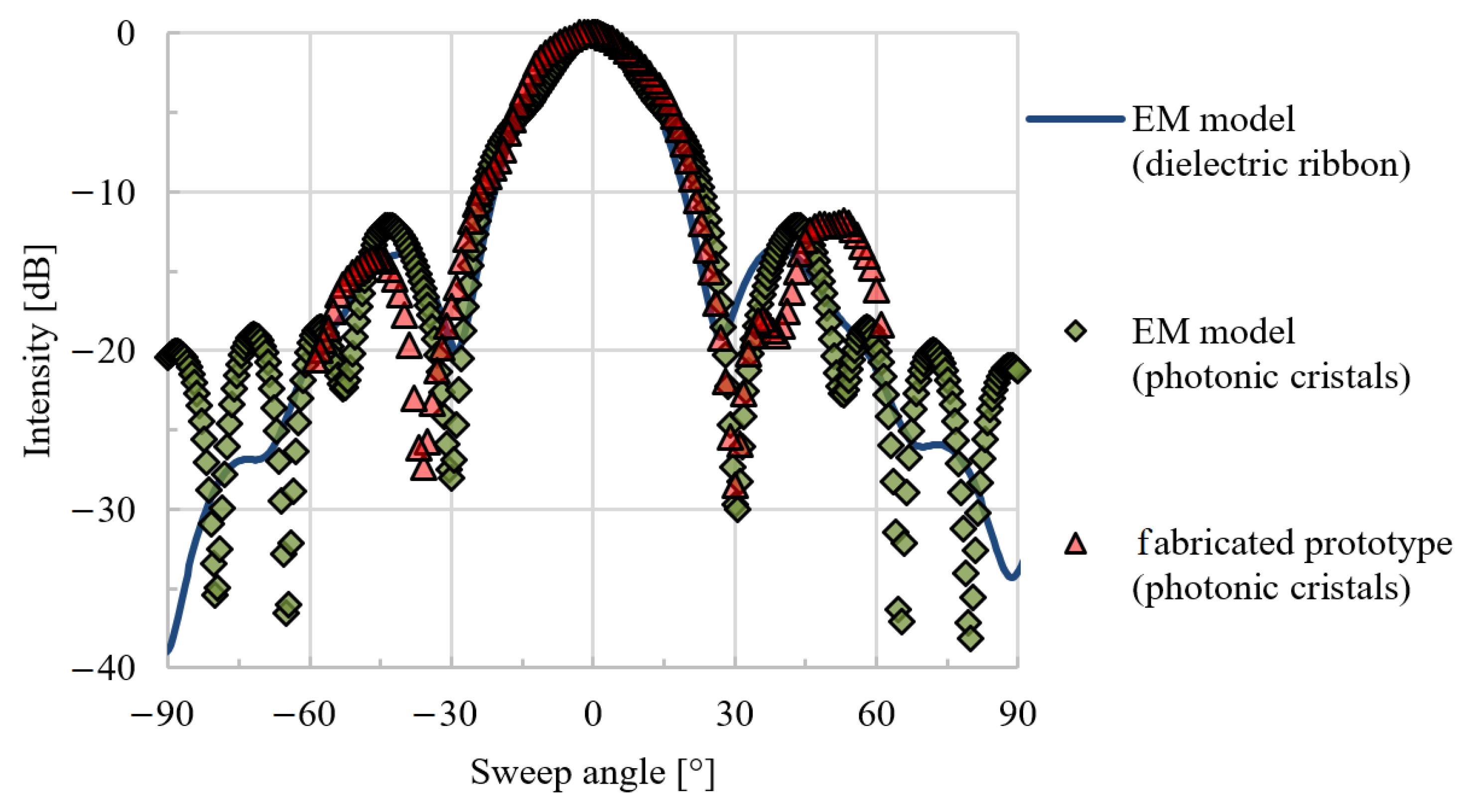
3.1. EM Simulations
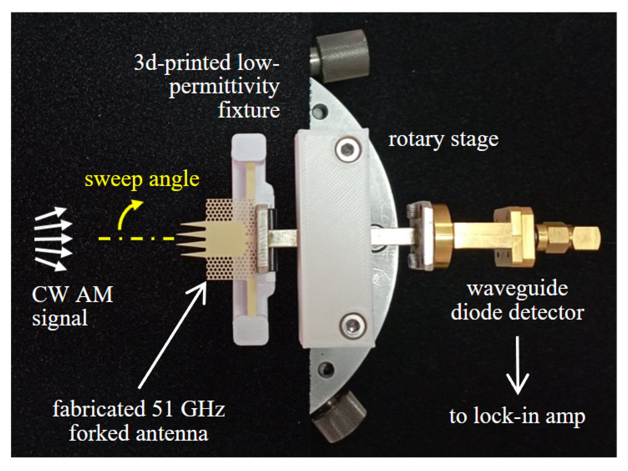
3.2. Prototyping
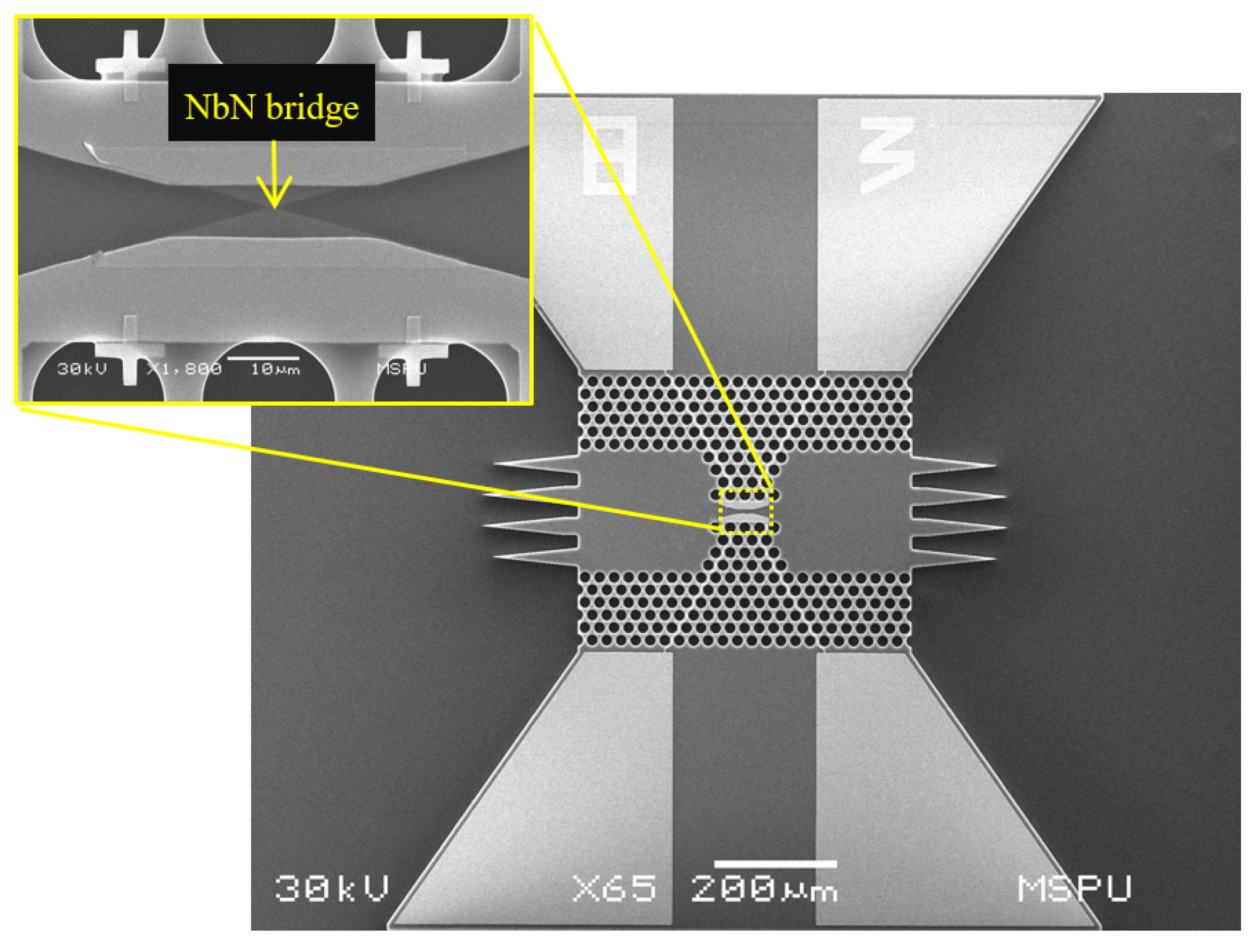
3.3. Cleanroom Process
- Deposition and patterning of an NbN microbridge integrated with Ti/Au bias lines on the topmost layer of SOI substrate;
- Fabrication of a hexagonal lattice of openings in the topmost layer by the Bosch process;
- Rear-side removal of the Si handle-wafer and SiO2.
4. Conclusions
Author Contributions
Funding
Institutional Review Board Statement
Informed Consent Statement
Data Availability Statement
Acknowledgments
Conflicts of Interest
Abbreviations
| THz | Terahertz |
| PIC | Photonic integrated circuit |
| PPDN | Photonic power distribution network |
| HEB | Hot electron bolometer |
| DRA | Dielectric rod antenna |
| LO | Local oscillator |
| SIS | Superconductor-insulator-superconductor |
| ISM | Interstellar medium |
| EM | Electromagnetic |
| MMIPC | Multimode interference power combiner |
| PCWG | Photonic crystal waveguide |
| TSL | Tapered slot line |
| 3d | Three-dimensional |
| AC | Alternating current |
| IR | Infrared |
| DBR | Distributed Bragg reflector |
| CW | Continuous waveform |
| AM | Amplitude modulation |
| SOI | Silicon-on-insulator |
References
- Yu, L.; Hao, L.; Meiqiong, T.; Jiaoqi, H.; Wei, L.; Jinying, D.; Xueping, C.; Weiling, F.; Yang, Z. The medical application of terahertz technology in non-invasive detection of cells and tissues: Opportunities and challenges. RSC Adv. 2019, 9, 9354–9363. [Google Scholar] [CrossRef] [PubMed]
- AlNabooda, M.O.; Shubair, R.M.; Rishani, N.R.; Aldabbagh, G. Terahertz spectroscopy and imaging for the detection and identification of illicit drugs. In Proceedings of the 2017 Sensors Networks Smart and Emerging Technologies (SENSET), Beirut, Lebanon, 12–14 September 2017; pp. 1–4. [Google Scholar]
- Ma, Y.; Li, J.; Han, Z.; Maeda, H.; Ma, Y. Bragg-mirror-assisted high-contrast plasmonic interferometers: Concept and potential in terahertz sensing. Nanomaterials 2020, 10, 1385. [Google Scholar] [CrossRef] [PubMed]
- Yang, K.; Li, J.; de la Chapelle, M.L.; Huang, G.; Wang, Y.; Zhang, J.; Xu, D.; Yao, J.; Yang, X.; Fu, W. A terahertz metamaterial biosensor for sensitive detection of microRNAs based on gold-nanoparticles and strand displacement amplification. Biosens. Bioelectron. 2021, 175, 112874. [Google Scholar] [CrossRef] [PubMed]
- Withayachumnankul, W.; Fujita, M.; Nagatsuma, T. Integrated silicon photonic crystals toward terahertz communications. Adv. Opt. Mater. 2018, 6, 1800401. [Google Scholar] [CrossRef]
- Kumar, A.; Gupta, M.; Pitchappa, P.; Wang, N.; Fujita, M.; Singh, R. Terahertz topological photonic integrated circuits for 6G and beyond: A Perspective. J. Appl. Phys. 2022, 132, 140901. [Google Scholar] [CrossRef]
- Jha, K.R.; Singh, G. Analysis of narrow terahertz microstrip transmission-line on multilayered substrate. J. Comput. Electron. 2011, 10, 186–194. [Google Scholar] [CrossRef]
- Cao, L.; Grimault-Jacquin, A.S.; Aniel, F. Comparison and optimization of dispersion, and losses of planar waveguides on benzocyclobutene (BCB) at THz frequencies: Coplanar waveguide (CPW), microstrip, stripline and slotline. Prog. Electromagn. Res. B 2013, 56, 161–183. [Google Scholar] [CrossRef]
- Koala, R.A.; Fujita, M.; Nagatsuma, T. Nanophotonics-inspired all-silicon waveguide platforms for terahertz integrated systems. Nanophotonics 2022, 11, 1741–1759. [Google Scholar] [CrossRef]
- Sengupta, K.; Nagatsuma, T.; Mittleman, D.M. Terahertz integrated electronic and hybrid electronic–photonic systems. Nat. Electron. 2018, 1, 622–635. [Google Scholar] [CrossRef]
- Martini, F.; Cibella, S.; Gaggero, A.; Mattioli, F.; Leoni, R. Waveguide integrated hot electron bolometer for classical and quantum photonics. Opt. Express 2021, 29, 7956–7965. [Google Scholar] [CrossRef]
- Karpov, A.; Miller, D.; Rice, F.; Stern, J.; Bumble, B.; LeDuc, H.; Zmuidzinas, J. Low Noise 1 THz–1.4 THz Mixers Using Nb/Al-AlN/NbTiN SIS Junctions. IEEE Trans. Appl. Supercond. 2007, 17, 343–346. [Google Scholar] [CrossRef]
- Mehdi, I.; Siles, J.V.; Lee, C.; Schlecht, E. THz diode technology: Status, prospects, and applications. Proc. IEEE 2017, 105, 990–1007. [Google Scholar] [CrossRef]
- Shurakov, A.; Lobanov, Y.; Goltsman, G. Superconducting hot-electron bolometer: From the discovery of hot-electron phenomena to practical applications. Supercond. Sci. Technol. 2015, 29, 023001. [Google Scholar] [CrossRef]
- Stacey, G.J. THz low resolution spectroscopy for astronomy. IEEE Trans. Terahertz Sci. Technol. 2011, 1, 241–255. [Google Scholar] [CrossRef]
- Silva, J.; Mirzaei, B.; Laauwen, W.; More, N.; Young, A.; Kulesa, C.; Walker, C.; Khalatpour, A.; Hu, Q.; Groppi, C.; et al. 4 × 2 HEB receiver at 4.7 THz for GUSTO. In Millimeter, Submillimeter, and Far-Infrared Detectors and Instrumentation for Astronomy IX; SPIE: Austin, TX, USA, 2018; Volume 10708, pp. 94–103. [Google Scholar]
- Wiedner, M.C.; Mehdi, I.; Baryshev, A.; Belitsky, V.; Desmaris, V.; DiGiorgio, A.M.; Gallego, J.D.; Gerin, M.; Goldsmith, P.; Helmich, F.; et al. A proposed heterodyne receiver for the origins space telescope. IEEE Trans. Terahertz Sci. Technol. 2018, 8, 558–571. [Google Scholar] [CrossRef]
- Shi, S.C.; Paine, S.; Yao, Q.J.; Lin, Z.H.; Li, X.X.; Duan, W.Y.; Matsuo, H.; Zhang, Q.; Yang, J.; Ashley, M.; et al. Terahertz and far-infrared windows opened at Dome A in Antarctica. Nat. Astron. 2016, 1, 0001. [Google Scholar] [CrossRef]
- Balanis, C.A. Antenna Theory: Analysis and Design; John Wiley & Sons: Hoboken, NJ, USA, 1997. [Google Scholar]
- Cheng, L.; Mao, S.; Li, Z.; Han, Y.; Fu, H. Grating couplers on silicon photonics: Design principles, emerging trends and practical issues. Micromachines 2020, 11, 666. [Google Scholar] [CrossRef]
- Bakke, T.; Sullivan, C.T.; Mukherjee, S.D. Polymeric optical spot-size transformer with vertical and lateral tapers. J. Light. Technol. 2002, 20, 1188. [Google Scholar] [CrossRef]
- James, J.R. Engineering approach to the design of tapered dielectric-rod and horn antennas. Radio Electron. Eng. 1972, 42, 251–259. [Google Scholar] [CrossRef]
- Shiau, Y. Dielectric rod antennas for millimeter-wave integrated circuits (short papers). IEEE Trans. Microw. Theory Tech. 1976, 24, 869–872. [Google Scholar] [CrossRef]
- Lobanov, Y.; Shcherbatenko, M.; Shurakov, A.; Rodin, A.V.; Klimchuk, A.; Nadezhdinsky, A.I.; Maslennikov, S.; Larionov, P.; Finkel, M.; Semenov, A.; et al. Heterodyne detection at near-infrared wavelengths with a superconducting NbN hot-electron bolometer mixer. Opt. Lett 2014, 39, 1429–1432. [Google Scholar] [CrossRef] [PubMed]
- Chau, Y.F.; Yang, T.J.; Lee, W.D. Coupling technique for efficient interfacing between silica waveguides and planar photonic crystal circuits. Appl. Opt. 2004, 43, 6656–6663. [Google Scholar] [CrossRef] [PubMed]
- Soldano, L.B.; Pennings, E.C. Optical multi-mode interference devices based on self-imaging: Principles and applications. J. Light. Technol. 1995, 13, 615–627. [Google Scholar] [CrossRef]
- Tesmer, H.; Reese, R.; Polat, E.; Nickel, M.; Jakoby, R.; Maune, H. Fully dielectric rod antenna arrays with integrated power divider. Frequenz 2019, 73, 367–377. [Google Scholar] [CrossRef]
- Prikhodko, A.; Belikov, I.; Lvov, A.; Shurakov, A.; Goltsman, G. Millimeter wave photonic crystal waveguides fabricated via direct machining. St. Petersburg State Polytech. Univ. J. Phys. Math. 2022, 15, 345–349. [Google Scholar]


| [μm] | [μm] | [μm] | [] | [μm] | s [μm] | [μm] | [μm] | [μm] |
|---|---|---|---|---|---|---|---|---|
| 27 | 32 | 70.9 | 146 | 11.9 | 21 | 10 | 8 | 6 |
| [μm] | [μm] | [μm] | [μm] | [μm] | [] | d [μm] |
|---|---|---|---|---|---|---|
| 27 | 205.6 | 222.2 | 30.6 | 19.5 | 12 | 55.5 |
Disclaimer/Publisher’s Note: The statements, opinions and data contained in all publications are solely those of the individual author(s) and contributor(s) and not of MDPI and/or the editor(s). MDPI and/or the editor(s) disclaim responsibility for any injury to people or property resulting from any ideas, methods, instructions or products referred to in the content. |
© 2023 by the authors. Licensee MDPI, Basel, Switzerland. This article is an open access article distributed under the terms and conditions of the Creative Commons Attribution (CC BY) license (https://creativecommons.org/licenses/by/4.0/).
Share and Cite
Shurakov, A.; Belikov, I.; Prikhodko, A.; Ershova, M.; Goltsman, G. Superconducting Electronic–Photonic Platform for HEB-Based Terahertz Spectrometers. Appl. Sci. 2023, 13, 5892. https://doi.org/10.3390/app13105892
Shurakov A, Belikov I, Prikhodko A, Ershova M, Goltsman G. Superconducting Electronic–Photonic Platform for HEB-Based Terahertz Spectrometers. Applied Sciences. 2023; 13(10):5892. https://doi.org/10.3390/app13105892
Chicago/Turabian StyleShurakov, Alexander, Ivan Belikov, Anatoliy Prikhodko, Margarita Ershova, and Gregory Goltsman. 2023. "Superconducting Electronic–Photonic Platform for HEB-Based Terahertz Spectrometers" Applied Sciences 13, no. 10: 5892. https://doi.org/10.3390/app13105892