
Effects of Adding Alkali Metals and Organic Cations to Cu-Based Perovskite Solar Cells

 , ,
, ,
Abstract
:1. Introduction
2. Computational Conditions and Experimental Methods
3. Results and Discussion
4. Conclusions
Author Contributions
Funding
Institutional Review Board Statement
Informed Consent Statement
Data Availability Statement
Conflicts of Interest
References
- Wang, F.; Yang, M.; Yang, S.; Qu, X.; Yang, L.; Fan, L.; Yang, J.; Rosei, F. Iodine-assisted antisolvent engineering for stable perovskite solar cells with efficiency >21.3%. Nano Energy 2020, 67, 104224. [Google Scholar] [CrossRef]
- Mingyu, J.; Choi, I.W.; Go, E.M.; Cho, Y.; Kim, M.; Byongkyu, L.; Seonghun, J.; Yimhyun, J.; Choi, H.W.; Lee, J.; et al. Stable perovskite solar cells with efficiency exceeding 24.8% and 0.3-V voltage loss. Science 2020, 369, 1615–1620. [Google Scholar] [CrossRef]
- Kim, G.; Min, H.; Lee, S.K.; Lee, Y.D.; Yoon, M.S.; Seok, I.S. Impact of strain relaxation on performance of α-formamidinium lead iodide perovskite solar cells. Science 2020, 370, 108. [Google Scholar] [CrossRef]
- Popov, G.; Mattinen, M.; Kemell, M.L.; Ritala, M.; Leskelä, M. Scalable route to the fabrication of CH3NH3PbI3 perovskite thin films by electrodeposition and vapor conversion. ACS Omega 2016, 1, 1296–1306. [Google Scholar] [CrossRef]
- Zanca, C.; Piazza, V.; Agnello, S.; Patella, B.; Ganci, F.; Aiello, G.; Piazza, S.; Sunseri, C.; Inguanta, R. Controlled solution-based fabrication of perovskite thin films directly on conductive substrate. Thin Solid Film. 2021, 733, 138806. [Google Scholar] [CrossRef]
- Duan, C.; Wen, Q.; Fan, Y.; Li, J.; Liu, Z.; Yan, K. Improving the stability and scalability of all-inorganic inverted CsPbI2Br perovskite solar cell. Energy Chem. 2022, 68, 176–183. [Google Scholar] [CrossRef]
- Shen, L.; Zhu, T.; Zhang, X.; Gong, K.; Wang, H.; Gong, X. Bulk heterojunction perovskite solar cells incorporated with p-type low optical gap conjugated polymers. Nano Energy 2022, 93, 106907. [Google Scholar] [CrossRef]
- Zhang, Y.; Pathak, R.; Zheng, D.; Cheng, P.; Chen, T.; Chen, X.; Wei, K.; Wang, R.; Wu, F. Synthesis of cesium bismuth iodide perovskite using toluene as anti-solvent with higher photocurrent response. Mater. Lett. 2022, 310, 131514. [Google Scholar] [CrossRef]
- Bohr, C.; Le, K.; Fischer, T.; Mathur, S. Triaxial perovskite composite fibers spinning the way to flexible solar cells. Adv. Eng. Mater. 2021, 24, 2100773. [Google Scholar] [CrossRef]
- Arora, N.; Dar, M.I.; Hinderhofer, A.; Pellet, N.; Schreiber, F.; Zakeeruddin, S.M.; Grätzel, M. Perovskite solar cells with CuSCN hole extraction layers yield stabilized efficiencies greater than 20%. Science 2017, 358, 768–771. [Google Scholar] [CrossRef] [Green Version]
- Shirahata, Y.; Oku, T. Microstructures, optical and photovoltaic properties of CH3NH3PbI3(1−x)Clx perovskite films with CuSCN additive. Mater. Res. Express 2018, 5, 055504. [Google Scholar] [CrossRef]
- Islam, M.A.; Wahab, Y.A.; Khandaker, M.U.; Alsubaie, A.; Almalki, A.S.A.; Bradley, D.A.; Amin, N. High mobility reactive sputtered CuxO thin film for highly efficient and stable perovskite solar cells. Crystals 2021, 11, 389. [Google Scholar] [CrossRef]
- Salah, M.M.; Abouelatta, M.; Shaker, A.; Hassan, K.M.; Saeed, A. A comprehensive simulation study of hybrid halide perovskite solar cell with copper oxide as HTM. Semicond. Sci. Technol. 2019, 34, 115009. [Google Scholar] [CrossRef]
- Haider, S.Z.; Anwar, H.; Wang, M. A comprehensive device modelling of perovskite solar cell with inorganic copper iodide as hole transport material. Semicond. Sci. Technol. 2018, 33, 035001. [Google Scholar] [CrossRef] [Green Version]
- Pitriana, P.; Wungu, T.D.K.; Herman; Hidayat, R. The characteristics of band structures and crystal binding in all-inorganic perovskite APbBr3 studied by the first principle calculations using the density functional theory (DFT) method. Results Phys. 2019, 15, 102592. [Google Scholar] [CrossRef]
- Chang, C.; Zou, X.; Cheng, J.; Ling, T.; Yao, Y.; Chen, D. Applied trace alkali metal elements for semiconductor property modulation of perovskite thin films. Molecules 2019, 24, 4039. [Google Scholar] [CrossRef] [PubMed] [Green Version]
- Xiang, S.; Li, W.; Wei, Y.; Liu, J.; Liu, H.; Zhu, L.; Yang, S.; Chen, H. Natrium doping pushes the efficiency of carbon-based CsPbI3 perovskite solar cells to 10.7%. iScience 2019, 15, 156–164. [Google Scholar] [CrossRef] [Green Version]
- Qiao, L.; Fang, W.H.; Long, R.; Prezhdo, O.V. Alkali metals extend carrier lifetimes in lead halide perovskites by passivating and eliminating halide interstitial defects. Angew. Chem. 2020, 132, 4714–4720. [Google Scholar] [CrossRef]
- Zhao, W.; Yao, Z.; Yu, F.; Yang, D.; Liu, S. Alkali metal doping for improved CH3NH3PbI3 perovskite solar cells. Adv. Sci. 2018, 5, 1700131. [Google Scholar] [CrossRef] [Green Version]
- Machiba, H.; Oku, T.; Kishimoto, T.; Ueoka, N.; Suzuki, A. Fabrication and evaluation of K-doped MA0.8FA0.1K0.1PbI3(Cl) perovskite solar cells. Chem. Phys. Lett. 2019, 730, 117–123. [Google Scholar] [CrossRef]
- Oku, T.; Kandori, S.; Taguchi, M.; Suzuki, A.; Okita, M.; Minami, S.; Fukunishi, S.; Tachikawa, T. Polysilane-inserted methylammonium lead iodide perovskite solar cells doped with formamidinium and potassium. Energies 2020, 13, 4776. [Google Scholar] [CrossRef]
- Kandori, S.; Oku, T.; Nishi, K.; Kishimoto, T.; Ueoka, N.; Suzuki, A. Fabrication and characterization of potassium- and formamidinium-added perovskite solar cells. J. Ceram. Soc. Jpn. 2020, 128, 805. [Google Scholar] [CrossRef]
- Boopathi, K.M.; Mohan, R.; Huang, T.Y.; Budiawan, W.; Lin, M.Y.; Lee, C.H.; Ho, K.C.; Chu, C.W. Synergistic improvements in stability and performance of lead iodide perovskite solar cells incorporating salt additives. J. Mater. Chem. A 2016, 4, 1591. [Google Scholar] [CrossRef]
- Wang, K.L.; Wang, R.; Wang, Z.K.; Li, M.; Zhang, Y.; Ma, H.; Liao, L.S.; Yang, Y. Tailored phase transformation of CsPbI2Br films by copper (II) bromide for high-performance all-inorganic perovskite solar cells. Nano Lett. 2019, 19, 5176–5184. [Google Scholar] [CrossRef]
- Li, M.; Wang, Z.K.; Zhuo, M.P.; Hu, Y.; Hu, K.H.; Ye, Q.Q.; Jain, S.M.; Yang, Y.G.; Gao, X.Y.; Liao, L.S. Pb–Sn–Cu Ternary organometallic halide perovskite solar cells. Adv. Mater. 2018, 30, 1800258. [Google Scholar] [CrossRef] [PubMed]
- Elseman, A.M.; Shalan, A.E.; Sajid, S.; Rashad, M.M.; Hassan, A.M.; Li, M. Copper-substituted lead perovskite materials constructed with different halides for working (CH3NH3)2CuX4-based perovskite solar cells from experimental and theoretical view. ACS Appl. Mater. Interfaces 2018, 10, 11699–11707. [Google Scholar] [CrossRef] [PubMed]
- Jahandar, M.; Heo, J.H.; Song, C.E.; Kong, K.J.; Shin, W.S.; Lee, J.C.; Im, S.H.; Moon, S.J. Highly efficient metal halide substituted CH3NH3I(PbI2)1-X(CuBr2)X planar perovskite solar cells. Nano Energy 2016, 27, 330–339. [Google Scholar] [CrossRef]
- Ueoka, N.; Oku, T.; Suzuki, A. Additive effects of alkali metals on Cu-modified CH3NH3PbI3-δClδ photovoltaic devices. RSC Adv. 2019, 9, 24231–24240. [Google Scholar] [CrossRef] [Green Version]
- Ueoka, N.; Oku, T. Effects of co-addition of sodium chloride and copper (II) bromide to mixed-cation mixed-halide perovskite photovoltaic devices. ACS Appl. Energy Mater. 2020, 3, 7272–7283. [Google Scholar] [CrossRef]
- Ueoka, N.; Oku, T.; Suzuki, A. Effects of doping with Na, K, Rb, and formamidinium cations on (CH3NH3)0.99Rb0.01Pb0.99Cu0.01I3−x(Cl, Br)x perovskite photovoltaic cells. AIP Adv. 2020, 10, 125023. [Google Scholar] [CrossRef]
- Oku, T. Crystal structures of perovskite halide compounds used for solar cells. Rev. Adv. Mater. Sci. 2020, 59, 264–305. [Google Scholar] [CrossRef]
- Liu, D.; Li, Q.; Wu, K. Ethylammonium as an alternative cation for efficient perovskite solar cells from first-principles calculations. RSC Adv. 2019, 9, 7356. [Google Scholar] [CrossRef] [Green Version]
- Xiao, Z.; Yan, Y. Progress in theoretical study of metal halide perovskite solar cell materials. Adv. Energy Mater. 2017, 7, 1701136. [Google Scholar] [CrossRef]
- Jung, M.H. Formation of cubic perovskite alloy containing the ammonium cation of 2D perovskite for high performance solar cells with improved stability. RSC Adv. 2021, 11, 32590. [Google Scholar] [CrossRef]
- Nishi, K.; Oku, T.; Kishimoto, T.; Ueoka, N.; Suzuki, A. Photovoltaic characteristics of CH3NH3PbI3 perovskite solar cells added with ethylammonium bromide and formamidinium iodide. Coatings 2020, 10, 410. [Google Scholar] [CrossRef] [Green Version]
- Kishimoto, T.; Oku, T.; Suzuki, A.; Ueoka, N. Additive effects of guanidinium iodide on CH3NH3PbI3 perovskite solar cells. Phys. Status Solidi A 2021, 218, 2100396. [Google Scholar] [CrossRef]
- Mateen, M.; Arain, Z.; Liu, X.; Iqbal, A.; Ren, Y.; Zhang, X.; Liu, C.; Chen, Q.; Ma, S.; Ding, Y.; et al. Boosting optoelectronic performance of MAPbI3 perovskite solar cells via ethylammonium chloride additive engineering. Sci. China Mater. 2020, 63, 2477–2486. [Google Scholar] [CrossRef]
- Zhang, Y.; Kim, S.G.; Lee, D.; Shin, H.; Park, N.G. Bifacial stamping for high efficiency perovskite solar cells. RSC Energy Environ. Sci. 2019, 12, 308–321. [Google Scholar] [CrossRef]
- Dhar, A.; Dey, A.; Maiti, P.; Paul, P.K.; Roy, S.; Paul, S.; Vekariya, R.L. Fabrication and characterization of next generation nano-structured organo-lead halide-based perovskite solar cell. Ionics 2018, 24, 1–7. [Google Scholar] [CrossRef]
- Mohebpour, M.A.; Saffari, M.; Soleimani, H.R.; Tagani, M.B. High performance of mixed halide perovskite solar cells: Role of halogen atom and plasmonic nanoparticles on the ideal current density of cell. Phys. E 2018, 97, 282–289. [Google Scholar] [CrossRef] [Green Version]
- Lee, A.Y.; Park, D.Y.; Jeong, M.S. Correlational study of halogen tuning effect in hybrid perovskite single crystals with Raman scattering, X-ray diffraction, and absorption spectroscopy. J. Alloy. Compd. 2018, 738, 239–245. [Google Scholar] [CrossRef]
- Motta, C.; El-Mellouhi, F.; Sanvito, S. Charge carrier mobility in hybrid halide perovskites. Sci. Rep. 2015, 5, 12746. [Google Scholar] [CrossRef] [PubMed]
- Park, B.W.; Jain, S.M.; Zhang, X.; Hagfeldt, A.; Boschloo, G.; Edvinsson, T. Resonance raman and excitation energy dependent charge transfer mechanism in halide-substituted hybrid perovskite solar cells. ACS Nano 2015, 9, 2088–2101. [Google Scholar] [CrossRef] [PubMed]
- Li, Q.; Zhao, Y.; Zhou, W.; Han, Z.; Fu, R.; Lin, F.; Yu, D.; Zhao, Q. Halogen engineering for operationally stable perovskite solar cells via sequential deposition. Adv. Energy Mater. 2019, 9, 1902239. [Google Scholar] [CrossRef]
- Lin, P.Y.; Loganathan, A.; Raifuku, I.; Li, M.H.; Chiu, Y.Y.; Chang, S.T.; Fakharuddin, A.; Lin, C.F.; Guo, T.F.; Schmidt-Mende, L.; et al. Pseudo-halide perovskite solar cells. Adv. Energy Mater. 2021, 11, 2100818. [Google Scholar] [CrossRef]
- Suzuki, A.; Kitagawa, K.; Oku, T.; Okita, M.; Fukunishi, S.; Tachikawa, T. Additive effects of copper and alkali metal halides into methylammonium lead iodide perovskite solar cells. Electron. Mater. Lett. 2021, 1–11. [Google Scholar] [CrossRef]
- Suzuki, A.; Oku, T. Effects of mixed-valence states of Eu-doped FAPbI3 perovskite crystals studied by first-principles calculation. Mater. Adv. 2021, 2, 2609–2616. [Google Scholar] [CrossRef]
- Suzuki, A.; Oe, M.; Oku, T. Fabrication and characterization of Ni-, Co-, and Rb-incorporated CH3NH3PbI3 perovskite solar cells. J. Electron. Mater. 2021, 50, 1980–1995. [Google Scholar] [CrossRef]
- Oku, T.; Zushi, M.; Imanishi, Y.; Suzuki, A.; Suzuki, K. Microstructures and photovoltaic properties of perovskite-type CH3NH3PbI3 compounds. Appl. Phys. Express 2014, 7, 121601. [Google Scholar] [CrossRef]
- Oku, T.; Ohishi, Y.; Ueoka, N. Highly (100)-oriented CH3NH3PbI3(Cl) perovskite solar cells prepared with NH4Cl using an air blow method. RSC Adv. 2018, 8, 10389–10395. [Google Scholar] [CrossRef] [Green Version]
- Taguchi, M.; Suzuki, A.; Oku, T.; Ueoka, N.; Minami, S.; Okita, M. Effects of annealing temperature on decaphenylcyclopentasilane-inserted CH3NH3PbI3 perovskite solar cells. Chem. Phys. Lett. 2019, 737, 136822. [Google Scholar] [CrossRef]
- Oku, T.; Taguchi, M.; Kandori, S.; Suzuki, A.; Okita, M.; Minami, S.; Fukunishi, S.; Tachikawa, T. Effects of polysilane addition to chlorobenzene and high temperature annealing on CH3NH3PbI3 perovskite photovoltaic devices. Coatings 2021, 11, 665. [Google Scholar] [CrossRef]
- Suzuki, A.; Taguchi, M.; Oku, T.; Okita, M.; Minami, S.; Fukunishi, S.; Tachikawa, T. Additive effects of methyl ammonium bromide or formamidinium bromide in methylammonium lead iodide perovskite solar cells using decaphenylcyclopentasilane. J. Mater. Sci. Mater. Electron. 2021, 32, 26449–26464. [Google Scholar] [CrossRef]
- Ono, I.; Oku, T.; Suzuki, A.; Asakawa, Y.; Terada, S.; Okita, M.; Fukunishi, S.; Tachikawa, T. Fabrication and characterization of CH3NH3PbI3 solar cells with added guanidinium and inserted with decaphenylpentasilane. Jpn. J. Appl. Phys. 2022, 61, SB1024. [Google Scholar] [CrossRef]
- Huang, L.; Hu, Z.; Xu, J.; Zhang, K.; Zhang, J.; Zhu, Y. Multi-step slow annealing perovskite films for high performance planar perovskite solar cells. Sol. Energy Mater. Sol. Cells 2015, 141, 377–382. [Google Scholar] [CrossRef]


| Total Energy (keV) | Energy Gap (eV) | me*/m0 | mh*/m0 | |
|---|---|---|---|---|
| MAPbI3 | −3.50 | 1.51 | 0.071 | 0.100 |
| MAPbBr3 | −3.66 | 2.26 | 0.224 | 0.100 |
| MAPbCl3 | −3.78 | 2.75 | 0.144 | 0.462 |
| MAPbClBrI | −3.64 | 2.03 | 0.092 | 0.102 |
| MACuI3 | −2.52 | 1.48 | 0.136 | 0.079 |
| EAPbI3 | −3.68 | 1.43 | 0.076 | 0.104 |
| EACuI3 | −2.71 | 1.42 | 0.097 | 0.080 |
| NaPbI3 | −2.99 | 1.06 | 0.077 | 0.062 |
| KPbI3 | −3.00 | 1.04 | 0.068 | 0.062 |
| RbPbI3 | −3.00 | 1.03 | 0.067 | 0.062 |
| CsPbI3 | −3.00 | 1.00 | 0.067 | 0.061 |
| Total Energy (keV) | Energy Gap (eV) | me*/m0 | mh*/m0 | |
|---|---|---|---|---|
| MA0.875EA0.125PbI3 | −3.52 | 1.49 | 0.228 | 0.199 |
| MA0.875EA0.125Pb0.875Cu0.125I3 | −3.39 | 1.00 | 0.266 | 0.352 |
| MA0.750EA0.125Na0.125Pb0.875Cu0.125I3 | −3.32 | 1.04 | 0.241 | 0.355 |
| MA0.750EA0.125Na0.125Pb0.875Cu0.125I2.25Br0.75 | −3.36 | 1.30 | 0.250 | 0.490 |
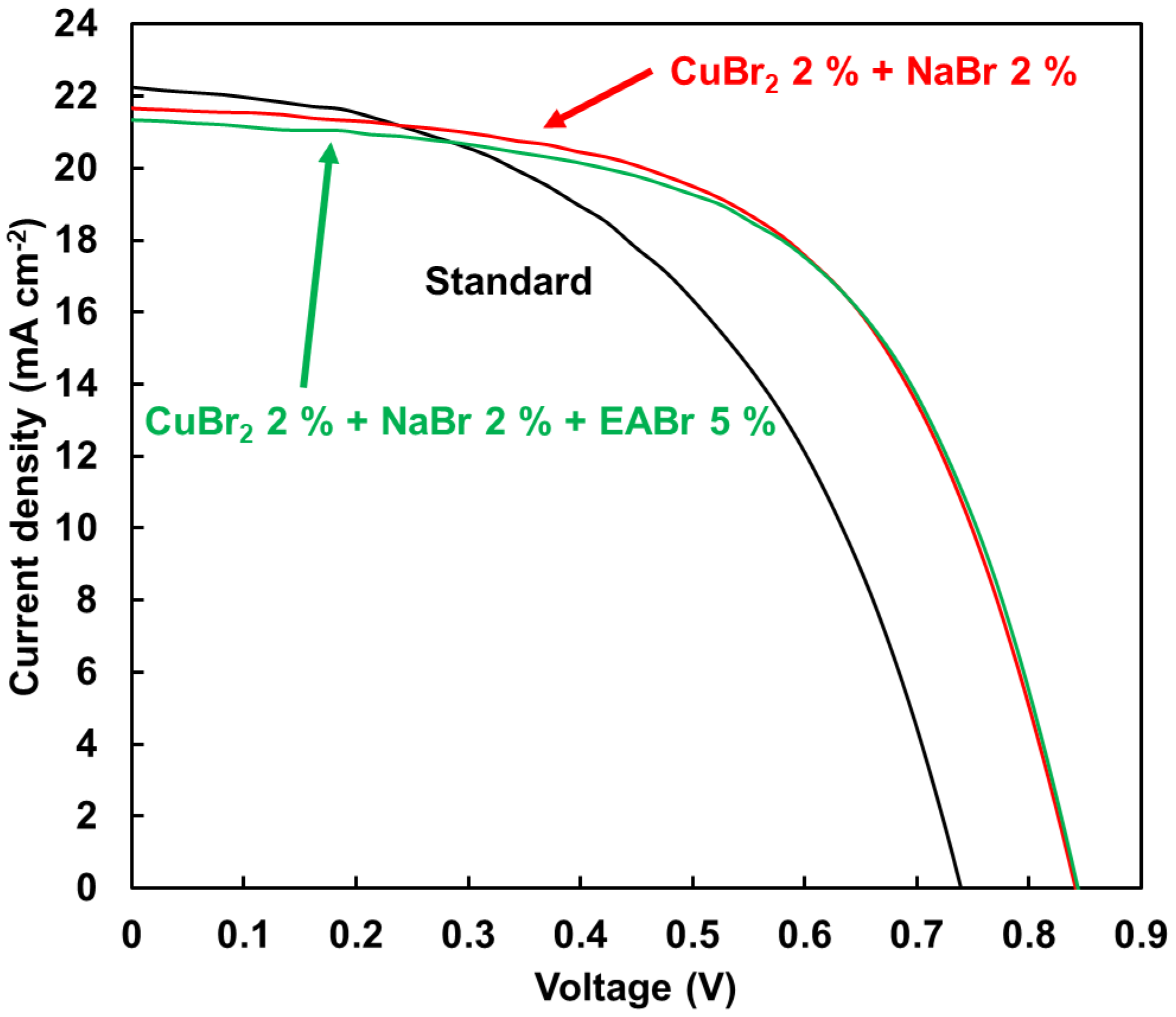
| Devices | JSC (mA cm−2) | VOC (V) | FF | RS (Ω cm2) | RSh (Ω cm2) | η (%) | ηave (%) | Eg |
|---|---|---|---|---|---|---|---|---|
| Standard | 22.2 | 0.739 | 0.497 | 4.18 | 383 | 8.17 | 5.82 | 1.55 |
| Cu 2% + Na 2% | 21.7 | 0.841 | 0.578 | 5.93 | 594 | 10.5 | 8.36 | 1.56 |
| Cu 2% + Na 2% + EA 2.5% | 20.0 | 0.811 | 0.559 | 6.55 | 604 | 9.08 | 7.20 | 1.56 |
| Cu 2% + Na 2% + EA 5% | 21.3 | 0.843 | 0.585 | 5.12 | 558 | 10.5 | 8.67 | 1.57 |
| Cu 2 + Na 2% + EA 10% | 16.1 | 0.824 | 0.586 | 5.29 | 445 | 7.78 | 5.77 | 1.57 |
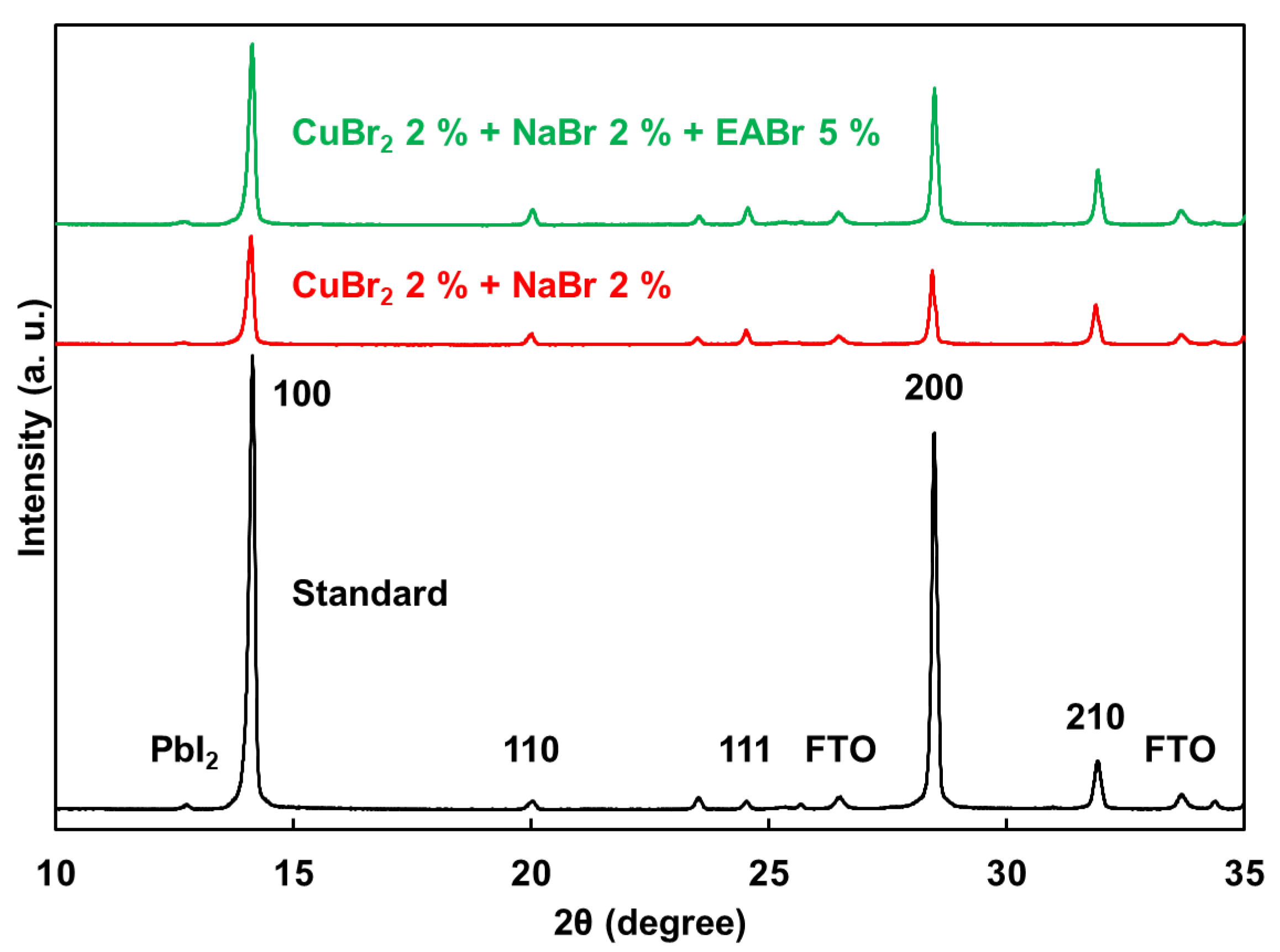
| Devices | I100/I210 | Lattice Constant (Å) | Crystallite Size (Å) |
|---|---|---|---|
| Standard | 8.7 | 6.262 (1) | 697 |
| CuBr2 2% NaBr 2% | 2.6 | 6.271 (1) | 679 |
| Cu Na 2% EABr 5% | 3.1 | 6.261(1) | 674 |
Publisher’s Note: MDPI stays neutral with regard to jurisdictional claims in published maps and institutional affiliations. |
© 2022 by the authors. Licensee MDPI, Basel, Switzerland. This article is an open access article distributed under the terms and conditions of the Creative Commons Attribution (CC BY) license (https://creativecommons.org/licenses/by/4.0/).
Share and Cite
Okumura, R.; Oku, T.; Suzuki, A.; Okita, M.; Fukunishi, S.; Tachikawa, T.; Hasegawa, T. Effects of Adding Alkali Metals and Organic Cations to Cu-Based Perovskite Solar Cells. Appl. Sci. 2022, 12, 1710. https://doi.org/10.3390/app12031710
Okumura R, Oku T, Suzuki A, Okita M, Fukunishi S, Tachikawa T, Hasegawa T. Effects of Adding Alkali Metals and Organic Cations to Cu-Based Perovskite Solar Cells. Applied Sciences. 2022; 12(3):1710. https://doi.org/10.3390/app12031710
Chicago/Turabian StyleOkumura, Riku, Takeo Oku, Atsushi Suzuki, Masanobu Okita, Sakiko Fukunishi, Tomoharu Tachikawa, and Tomoya Hasegawa. 2022. "Effects of Adding Alkali Metals and Organic Cations to Cu-Based Perovskite Solar Cells" Applied Sciences 12, no. 3: 1710. https://doi.org/10.3390/app12031710