
Methylammonium Lead Tri-Iodide Perovskite Solar Cells with Varying Equimolar Concentrations of Perovskite Precursors


Abstract
:1. Introduction
2. Materials and Methods
2.1. Materials
2.2. Morphology Characterization
2.3. Optical Characterization
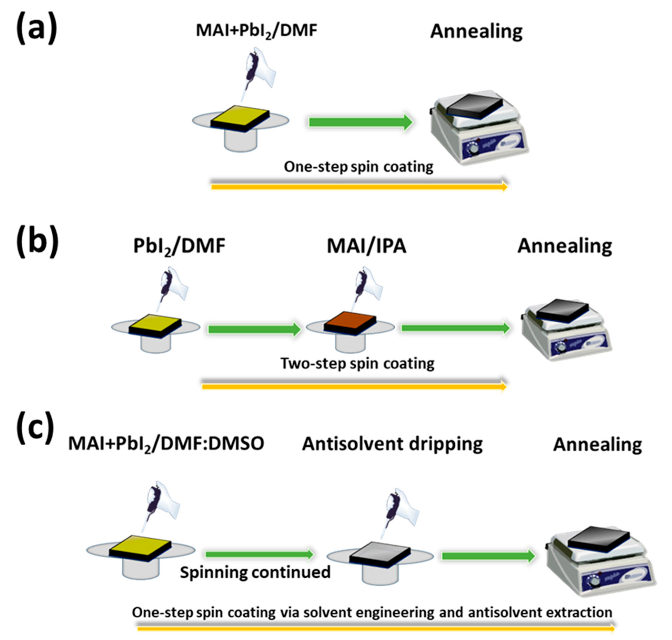
2.4. Device Fabrication
2.5. PSC Device Characterization
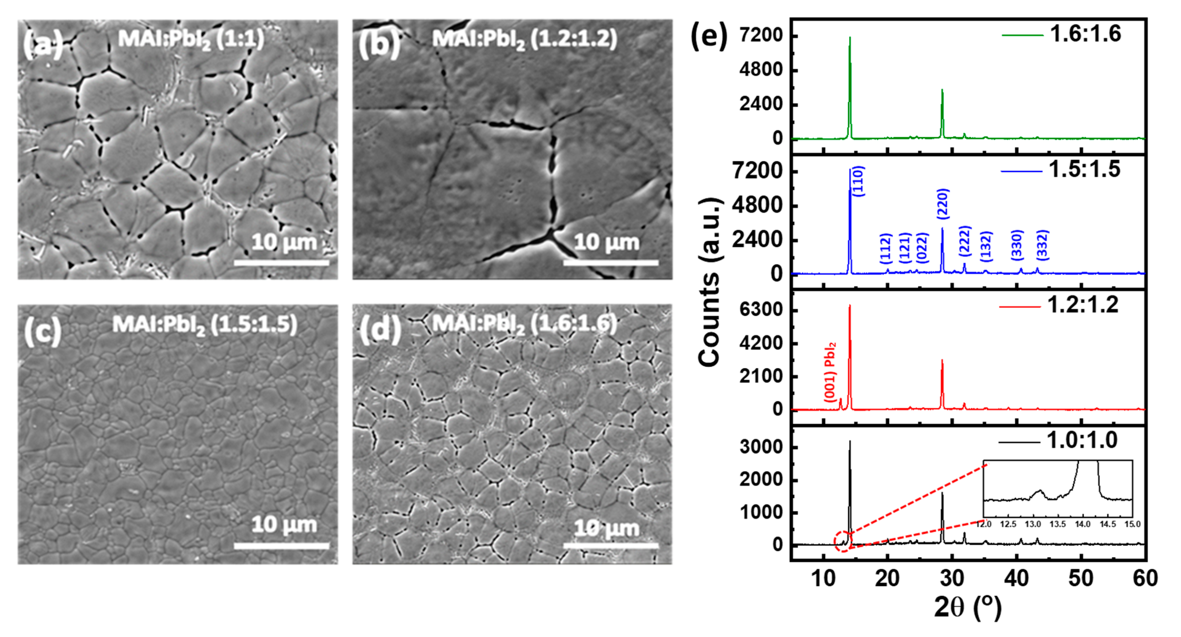
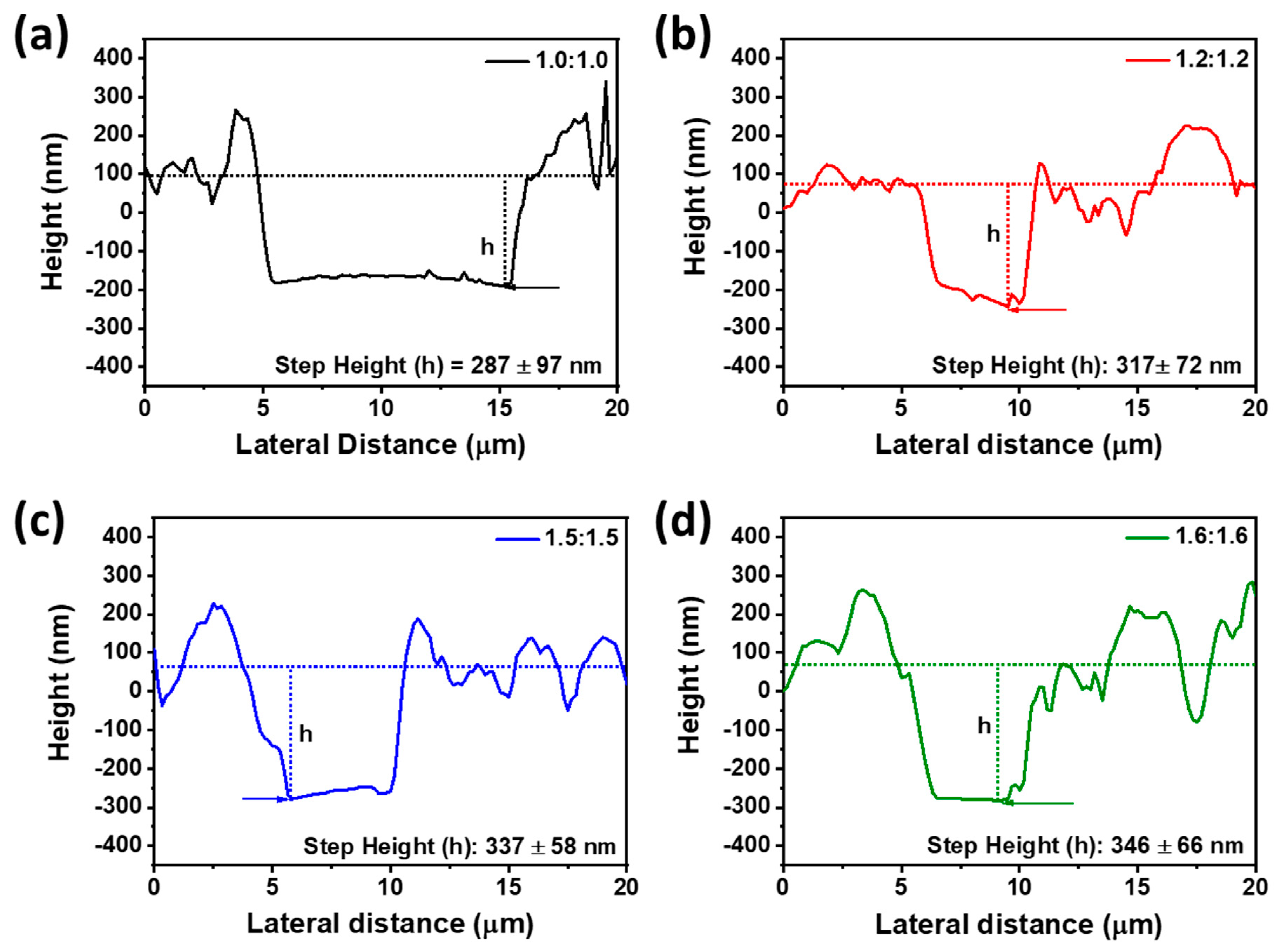
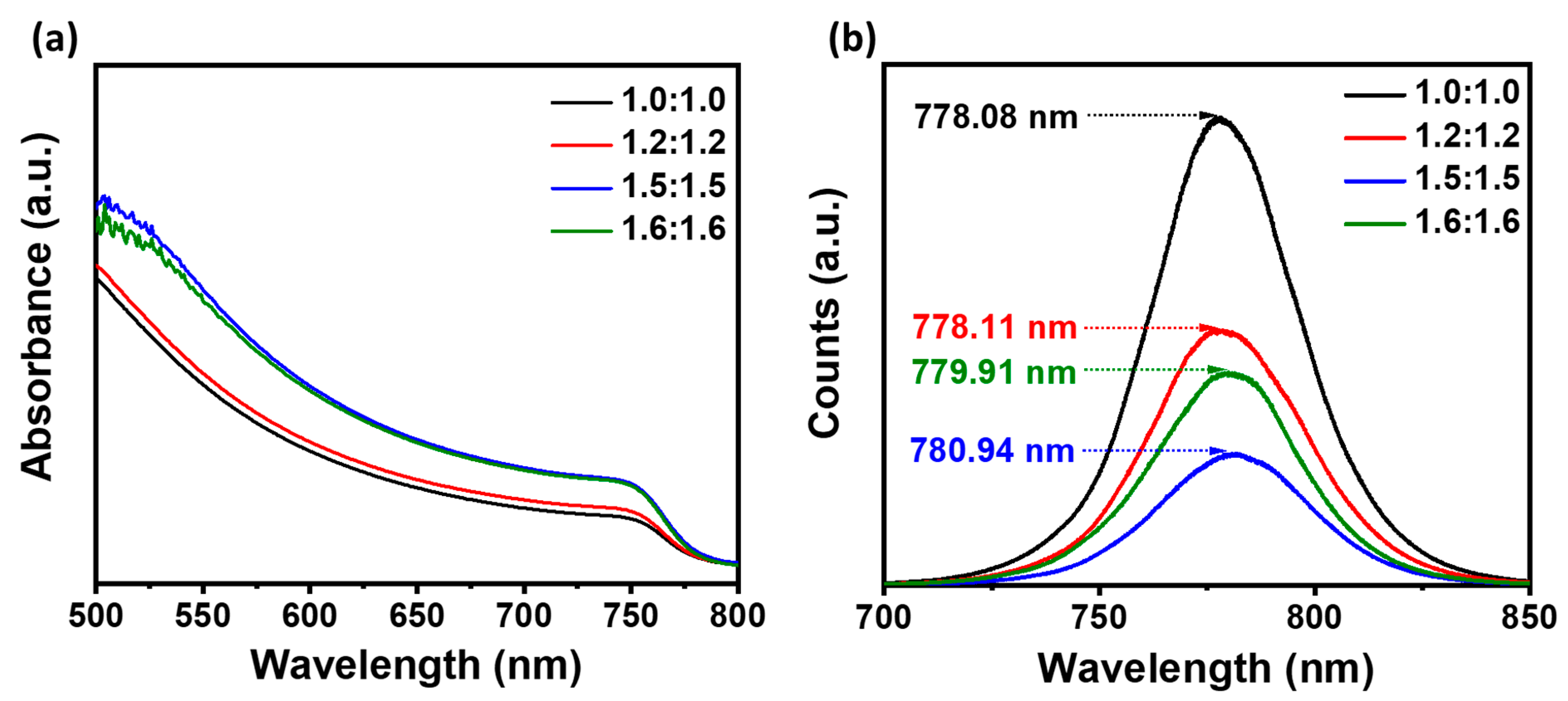
3. Results and Discussion
4. Conclusions
Author Contributions
Funding
Institutional Review Board Statement
Informed Consent Statement
Data Availability Statement
Acknowledgments
Conflicts of Interest
References
- Novoselov, K.S.; Geim, A.K.; Morozov, S.V.; Jiang, D.; Zhang, Y.; Dubonos, S.V.; Grigorieva, I.V.; Firsov, A.A. Electric Field in Atomically Thin Carbon Films. Science 2004, 306, 666–669. [Google Scholar] [CrossRef] [PubMed] [Green Version]
- Jayaramulu, K.; Horn, M.; Schneemann, A.; Saini, H.; Bakandritsos, A.; Ranc, V.; Petr, M.; Stavila, V.; Narayana, C.; Scheibe, B.; et al. Covalent Graphene-MOF Hybrids for High-Performance Asymmetric Supercapacitors. Adv. Mater. 2021, 33, 202004560. [Google Scholar] [CrossRef] [PubMed]
- Min, M.; Sakri, S.; Saenz, G.A.; Kaul, A.B. Photophysical Dynamics in Semiconducting Graphene Quantum Dots Integrated with 2D MoS2 for Optical Enhancement in the near UV. ACS Appl. Mater. Interfaces 2021, 13, 5379–5389. [Google Scholar] [CrossRef]
- Mehta, R.K.; Kaul, A.B. Black Phosphorus-Molybdenum Disulfide Hetero-Junctions Formed with Ink-Jet Printing for Potential Solar Cell Applications with Indium-Tin-Oxide. Crystals 2021, 11, 560. [Google Scholar] [CrossRef]
- Park, N.G. Perovskite Solar Cells: An Emerging Photovoltaic Technology. Mater. Today 2015, 18, 65–72. [Google Scholar] [CrossRef]
- Lin, K.; Xing, J.; Quan, L.N.; de Arquer, F.P.G.; Gong, X.; Lu, J.; Xie, L.; Zhao, W.; Zhang, D.; Yan, C.; et al. Perovskite Light-Emitting Diodes with External Quantum Efficiency Exceeding 20 per Cent. Nature 2018, 562, 245–248. [Google Scholar] [CrossRef] [PubMed]
- Liu, P.; He, X.; Ren, J.; Liao, Q.; Yao, J.; Fu, H. Organic-Inorganic Hybrid Perovskite Nanowire Laser Arrays. ACS Nano 2017, 11, 5766–5773. [Google Scholar] [CrossRef]
- Yang, Y.; Dai, H.; Yang, F.; Zhang, Y.; Luo, D.; Zhang, X.; Wang, K.; Sun, X.W.; Yao, J. All-Perovskite Photodetector with Fast Response. Nanoscale Res. Lett. 2019, 14, 291. [Google Scholar] [CrossRef] [Green Version]
- Hossain, R.F.; Min, M.; Ma, L.C.; Sakri, S.R.; Kaul, A.B. Carrier Photodynamics in 2D Perovskites with Solution-Processed Silver and Graphene Contacts for Bendable Optoelectronics. npj 2D Mater. Appl. 2021, 5, 34. [Google Scholar] [CrossRef]
- Min, M.; Hossain, R.F.; Adhikari, N.; Kaul, A.B. Inkjet-Printed Organohalide 2D Layered Perovskites for High-Speed Photodetectors on Flexible Polyimide Substrates. ACS Appl. Mater. Interfaces 2020, 12, 10809–10819. [Google Scholar] [CrossRef] [PubMed]
- Huang, H.; Pradhan, B.; Hofkens, J.; Roeffaers, M.B.J.; Steele, J.A. Solar-Driven Metal Halide Perovskite Photocatalysis: Design, Stability, and Performance. ACS Energy Lett. 2020, 5, 1107–1123. [Google Scholar] [CrossRef]
- Singh, R.; Parashar, M.; Sandhu, S.; Yoo, K.; Lee, J.J. The Effects of Crystal Structure on the Photovoltaic Performance of Perovskite Solar Cells under Ambient Indoor Illumination. Sol. Energy 2021, 220, 43–50. [Google Scholar] [CrossRef]
- Parashar, M.; Singh, R.; Shukla, V.K. Fabrication of Perovskite Solar Cells in Ambient Conditions. Mater. Today Proc. 2019, 34, 654–657. [Google Scholar] [CrossRef]
- Stranks, S.D.; Eperon, G.E.; Grancini, G.; Menelaou, C.; Alcocer, M.J.P.; Leijtens, T.; Herz, L.M.; Petrozza, A.; Snaith, H.J. Electron-Hole Diffusion Lengths Exceeding 1 Micrometer in an Organometal Trihalide Perovskite Absorber. Science 2013, 342, 341–344. [Google Scholar] [CrossRef] [Green Version]
- Dong, Q.; Fang, Y.; Shao, Y.; Mulligan, P.; Qiu, J.; Cao, L.; Huang, J. Electron-Hole Diffusion Lengths > 175 Μm in Solution-Grown CH3NH3PbI3 Single Crystals. Science 2015, 347, 967–970. [Google Scholar] [CrossRef] [PubMed] [Green Version]
- Savenije, T.J.; Ponseca, C.S.; Kunneman, L.; Abdellah, M.; Zheng, K.; Tian, Y.; Zhu, Q.; Canton, S.E.; Scheblykin, I.G.; Pullerits, T.; et al. Thermally Activated Exciton Dissociation and Recombination Control the Carrier Dynamics in Organometal Halide Perovskite. J. Phys. Chem. Lett. 2014, 5, 2189–2194. [Google Scholar] [CrossRef] [Green Version]
- Wetzelaer, G.J.A.H.; Scheepers, M.; Sempere, A.M.; Momblona, C.; Ávila, J.; Bolink, H.J. Trap-Assisted Non-Radiative Recombination in Organic-Inorganic Perovskite Solar Cells. Adv. Mater. 2015, 27, 1837–1841. [Google Scholar] [CrossRef] [PubMed]
- Nazeeruddin, M.K.; Snaith, H. Methylammonium Lead Triiodide Perovskite Solar Cells: A New Paradigm in Photovoltaics. MRS Bull. 2015, 40, 641–645. [Google Scholar] [CrossRef] [Green Version]
- Liang, H.; Yuan, F.; Johnston, A.; Gao, C.; Choubisa, H.; Gao, Y.; Wang, Y.K.; Sagar, L.K.; Sun, B.; Li, P.; et al. High Color Purity Lead-Free Perovskite Light-Emitting Diodes via Sn Stabilization. Adv. Sci. 2020, 7, 1903213. [Google Scholar] [CrossRef] [Green Version]
- Younis, A.; Lin, C.H.; Guan, X.; Shahrokhi, S.; Huang, C.Y.; Wang, Y.; He, T.; Singh, S.; Hu, L.; Retamal, J.R.D.; et al. Halide Perovskites: A New Era of Solution-Processed Electronics. Adv. Mater. 2021, 33, 2005000. [Google Scholar] [CrossRef] [PubMed]
- Goldschmidt, V.M. Krystallbau Und Chemische Zusammensetzung. Ber. Dtsch. Chem. Ges. 1927, 60, 1263–1296. [Google Scholar] [CrossRef]
- Li, C.; Lu, X.; Ding, W.; Feng, L.; Gao, Y.; Guo, Z. Formability of ABX 3 (X = F, Cl, Br, I) Halide Perovskites. Acta Crystallogr. Sect. B Struct. Sci. 2008, 64, 702–707. [Google Scholar] [CrossRef]
- Stevenson, J.; Sorenson, B.; Subramaniam, V.H.; Raiford, J.; Khlyabich, P.P.; Loo, Y.L.; Clancy, P. Mayer Bond Order as a Metric of Complexation Effectiveness in Lead Halide Perovskite Solutions. Chem. Mater. 2017, 29, 2435–2444. [Google Scholar] [CrossRef]
- Hoang, M.T.; Ünlü, F.; Martens, W.; Bell, J.; Mathur, S.; Wang, H. Towards the Environmentally Friendly Solution Processing of Metal Halide Perovskite Technology. Green Chem. 2021, 23, 5302–5336. [Google Scholar] [CrossRef]
- Lee, J.W.; Park, N.G. Two-Step Deposition Method for High-Efficiency Perovskite Solar Cells. MRS Bull. 2015, 40, 654–659. [Google Scholar] [CrossRef]
- An, Q.; Sun, Q.; Weu, A.; Becker-Koch, D.; Paulus, F.; Arndt, S.; Stuck, F.; Hashmi, A.S.K.; Tessler, N.; Vaynzof, Y. Enhancing the Open-Circuit Voltage of Perovskite Solar Cells by up to 120 MV Using Π-Extended Phosphoniumfluorene Electrolytes as Hole Blocking Layers. Adv. Energy Mater. 2019, 9, 1901257. [Google Scholar] [CrossRef] [Green Version]
- Liu, C.; Yang, Y.; Syzgantseva, O.A.; Ding, Y.; Syzgantseva, M.A.; Zhang, X.; Asiri, A.M.; Dai, S.; Nazeeruddin, M.K. α-CsPbI3 Bilayers via One-Step Deposition for Efficient and Stable All-Inorganic Perovskite Solar Cells. Adv. Mater. 2020, 32, 2002632. [Google Scholar] [CrossRef]
- Jung, M.; Ji, S.G.; Kim, G.; Seok, S.I. Perovskite Precursor Solution Chemistry: From Fundamentals to Photovoltaic Applications. Chem. Soc. Rev. 2019, 48, 2011–2038. [Google Scholar] [CrossRef]
- Burschka, J.; Pellet, N.; Moon, S.J.; Humphry-Baker, R.; Gao, P.; Nazeeruddin, M.K.; Grätzel, M. Sequential Deposition as a Route to High-Performance Perovskite-Sensitized Solar Cells. Nature 2013, 499, 316–319. [Google Scholar] [CrossRef] [PubMed]
- Cohen, B.-E.; Gamliel, S.; Etgar, L. Parameters Influencing the Deposition of Methylammonium Lead Halide Iodide in Hole Conductor Free Perovskite-Based Solar Cells. APL Mater. 2014, 2, 081502. [Google Scholar] [CrossRef]
- Im, J.; Jang, I.-H.; Norman, P.; Michael, G.; Park, N.-G. Growth of CH3NH3PbI3 Cuboids with Controlled Size for High-Efficiency Perovskite Solar Cells. Nat. Nanotechnol. 2014, 9, 927–932. [Google Scholar] [CrossRef]
- Im, J.H.; Kim, H.S.; Park, N.G. Morphology-Photovoltaic Property Correlation in Perovskite Solar Cells: One-Step versus Two-Step Deposition of CH3NH3PbI3. APL Mater. 2014, 2, 081510. [Google Scholar] [CrossRef] [Green Version]
- Jeon, N.J.; Noh, J.H.; Kim, Y.C.; Yang, W.S.; Ryu, S.; Seok, S.I. Solvent Engineering for High-Performance Inorganic-Organic Hybrid Perovskite Solar Cells. Nat. Mater. 2014, 13, 897–903. [Google Scholar] [CrossRef] [PubMed]
- Tavakoli, M.M.; Yadav, P.; Prochowicz, D.; Sponseller, M.; Osherov, A.; Bulović, V.; Kong, J. Controllable Perovskite Crystallization via Antisolvent Technique Using Chloride Additives for Highly Efficient Planar Perovskite Solar Cells. Adv. Energy Mater. 2019, 9, 1803587. [Google Scholar] [CrossRef]
- Lee, J.W.; Kim, H.S.; Park, N.G. Lewis Acid-Base Adduct Approach for High Efficiency Perovskite Solar Cells. Acc. Chem. Res. 2016, 49, 311–319. [Google Scholar] [CrossRef]
- Taylor, A.D.; Sun, Q.; Goetz, K.P.; An, Q.; Schramm, T.; Hofstetter, Y.; Litterst, M.; Paulus, F.; Vaynzof, Y. A General Approach to High-Efficiency Perovskite Solar Cells by Any Antisolvent. Nat. Commun. 2021, 12, 1878. [Google Scholar] [CrossRef] [PubMed]
- Liu, S.; Guan, Y.; Sheng, Y.; Hu, Y.; Rong, Y.; Mei, A.; Han, H. A Review on Additives for Halide Perovskite Solar Cells. Adv. Energy Mater. 2020, 10, 1902492. [Google Scholar] [CrossRef]
- Chen, Z.; Turedi, B.; Alsalloum, A.Y.; Yang, C.; Zheng, X.; Gereige, I.; Alsaggaf, A.; Mohammed, O.F.; Bakr, O.M. Single-Crystal MAPbI3 Perovskite Solar Cells Exceeding 21% Power Conversion Efficiency. ACS Energy Lett. 2019, 4, 1258–1259. [Google Scholar] [CrossRef] [Green Version]
- Kim, B.; Kim, M.; Lee, J.H.; Seok, S.I. Enhanced Moisture Stability by Butyldimethylsulfonium Cation in Perovskite Solar Cells. Adv. Sci. 2020, 7, 1901840. [Google Scholar] [CrossRef] [Green Version]
- El-Henawey, M.I.; Gebhardt, R.S.; El-Tonsy, M.M.; Chaudhary, S. Organic solvent vapor treatment of lead iodide layers in the two-step sequential deposition of CH3NH3PbI3-based perovskite solar cells. J. Mater. Chem. A 2016, 4, 1947–1952. [Google Scholar] [CrossRef]
- Park, N.G. High Efficiency Perovskite Solar Cells: Materials and Devices Engineering. Trans. Electr. Electron. Mater. 2020, 21, 1–15. [Google Scholar] [CrossRef]
- Shalan, A.E.; Oshikiri, T.; Narra, S.; Elshanawany, M.M.; Ueno, K.; Wu, H.P.; Nakamura, K.; Shi, X.; Diau, E.W.G.; Misawa, H. Cobalt Oxide (CoOx) as an Efficient Hole-Extracting Layer for High-Performance Inverted Planar Perovskite Solar Cells. ACS Appl. Mater. Interfaces 2016, 8, 33592–33600. [Google Scholar] [CrossRef] [PubMed] [Green Version]
- Koster, L.J.A.; Mihailetchi, V.D.; Xie, H.; Blom, P.W.M. Origin of the Light Intensity Dependence of the Short-Circuit Current of Polymer/Fullerene Solar Cells. Appl. Phys. Lett. 2005, 87, 203502. [Google Scholar] [CrossRef] [Green Version]
- Sharma, A.; Singh, R.; Kini, G.P.; Hyeon Kim, J.; Parashar, M.; Kim, M.; Kumar, M.; Kim, J.S.; Lee, J.J. Side-Chain Engineering of Diketopyrrolopyrrole-Based Hole-Transport Materials to Realize High-Efficiency Perovskite Solar Cells. ACS Appl. Mater. Interfaces 2021, 13, 7405–7415. [Google Scholar] [CrossRef] [PubMed]
- Cowan, S.R.; Roy, A.; Heeger, A.J. Recombination in Polymer-Fullerene Bulk Heterojunction Solar Cells. Phys. Rev. B—Condens. Matter Mater. Phys. 2010, 82, 245207. [Google Scholar] [CrossRef] [Green Version]
- Christians, J.A.; Schulz, P.; Tinkham, J.S.; Schloemer, T.H.; Harvey, S.P.; Tremolet De Villers, B.J.; Sellinger, A.; Berry, J.J.; Luther, J.M. Tailored Interfaces of Unencapsulated Perovskite Solar Cells for >1000 Hour Operational Stability. Nat. Energy 2018, 3, 68–74. [Google Scholar] [CrossRef]
- Alsari, M.; Pearson, A.J.; Wang, J.T.W.; Wang, Z.; Montisci, A.; Greenham, N.C.; Snaith, H.J.; Lilliu, S.; Friend, R.H. Degradation Kinetics of Inverted Perovskite Solar Cells. Sci. Rep. 2018, 8, 5977. [Google Scholar] [CrossRef] [PubMed] [Green Version]


| MAPbI3 (MAI:PbI2) | Peak Position (θ) | FWHM (Radian) | Crystallite Size (nm) |
|---|---|---|---|
| 1.0:1.0 | 7.06 | 0.00337 | 43.4 |
| 1.2:1.2 | 7.05 | 0.00330 | 44.2 |
| 1.5:1.5 | 7.06 | 0.00303 | 48.1 |
| 1.6:1.6 | 7.06 | 0.00321 | 45.5 |
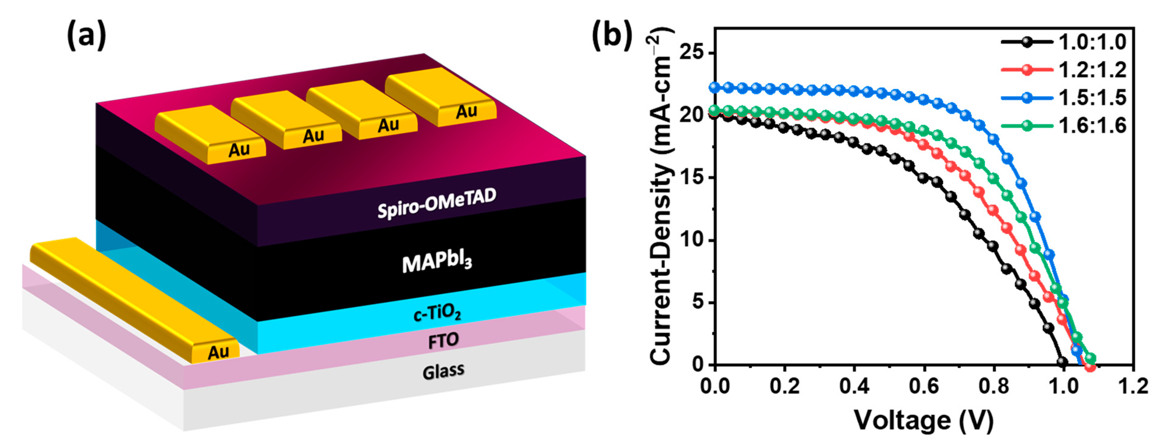
| MAPbI3 (MAI:PbI2) | PCE (%) | FF (%) | JSC (mA·cm−2) | VOC (V) | RSh (kΩ-cm2) | RS (Ω-cm2) |
|---|---|---|---|---|---|---|
| 1.0:1.0 | 9.32 | 46.38 | 20.06 | 1.00 | 0.22 | 15.58 |
| 1.2:1.2 | 10.98 | 50.75 | 20.34 | 1.06 | 1.36 | 19.33 |
| 1.5:1.5 | 14.56 | 62.58 | 22.21 | 1.05 | 3.49 | 8.82 |
| 1.6:1.6 | 12.25 | 55.50 | 20.39 | 1.08 | 1.29 | 16.29 |
Publisher’s Note: MDPI stays neutral with regard to jurisdictional claims in published maps and institutional affiliations. |
© 2021 by the authors. Licensee MDPI, Basel, Switzerland. This article is an open access article distributed under the terms and conditions of the Creative Commons Attribution (CC BY) license (https://creativecommons.org/licenses/by/4.0/).
Share and Cite
Parashar, M.; Kaul, A.B. Methylammonium Lead Tri-Iodide Perovskite Solar Cells with Varying Equimolar Concentrations of Perovskite Precursors. Appl. Sci. 2021, 11, 11689. https://doi.org/10.3390/app112411689
Parashar M, Kaul AB. Methylammonium Lead Tri-Iodide Perovskite Solar Cells with Varying Equimolar Concentrations of Perovskite Precursors. Applied Sciences. 2021; 11(24):11689. https://doi.org/10.3390/app112411689
Chicago/Turabian StyleParashar, Mritunjaya, and Anupama B. Kaul. 2021. "Methylammonium Lead Tri-Iodide Perovskite Solar Cells with Varying Equimolar Concentrations of Perovskite Precursors" Applied Sciences 11, no. 24: 11689. https://doi.org/10.3390/app112411689