1. Introduction
In recent years, lead halide perovskites (LHPs) have attracted much attention due to their success in various applications such as light emitting devices [
1], photovoltaic devices [
2], and photodetectors [
3]. The generic formula of a LHP is APbX
, where A can be an inorganic atom such as Cs, or an organic molecule such as methylammonium (MA) [CH
NH
], or formamidinuim (FA) [HC(NH
)
]. The species X is a halogen atom such as I, Cl, or Br. Perovskite materials have a three-dimensional network structure of Pb2
cations 6 coordinated with a halide species, and surrounded by 12 coordinated cations. Here we report the X-ray detection performance of organic LHP material containing the FA molecule. In FA-based LHPs the strength and the extension of the hydrogen bonds between the atoms (N-H-X) affects the microscopic dynamics of the organic cation [
4,
5,
6]. Pressure can alter the orientation of the organic cation and the length of the hydrogen bond between the atoms. At high temperatures, there is some evidence that formamidinium lead bromide (FAPbBr
) is more stable in humid and hot conditions when compared to methylammonium lead bromide (MAPbBr
) [
7,
8]. FAPbBr
may also possess some advantages in terms of device performance compared to MAPbBr
, due to its larger cation size where MA (R = 2.70 Å) and FA (R = 2.79 Å) [
9,
10], and the absence of room temperature phase transitions.
In this work we report the performance of polycrystalline FAPbBr
used as an energy integrating X-ray detector operating in a photoconductive mode. The polycrystalline perovskite detectors were fabricated using room temperature pressing of perovskite powders at high pressure. Due to the presence of high atomic number elements such as Pb, and a relatively high density of 4.1 g cm
, the X-ray detection efficiency of lead halide perovskites is high.
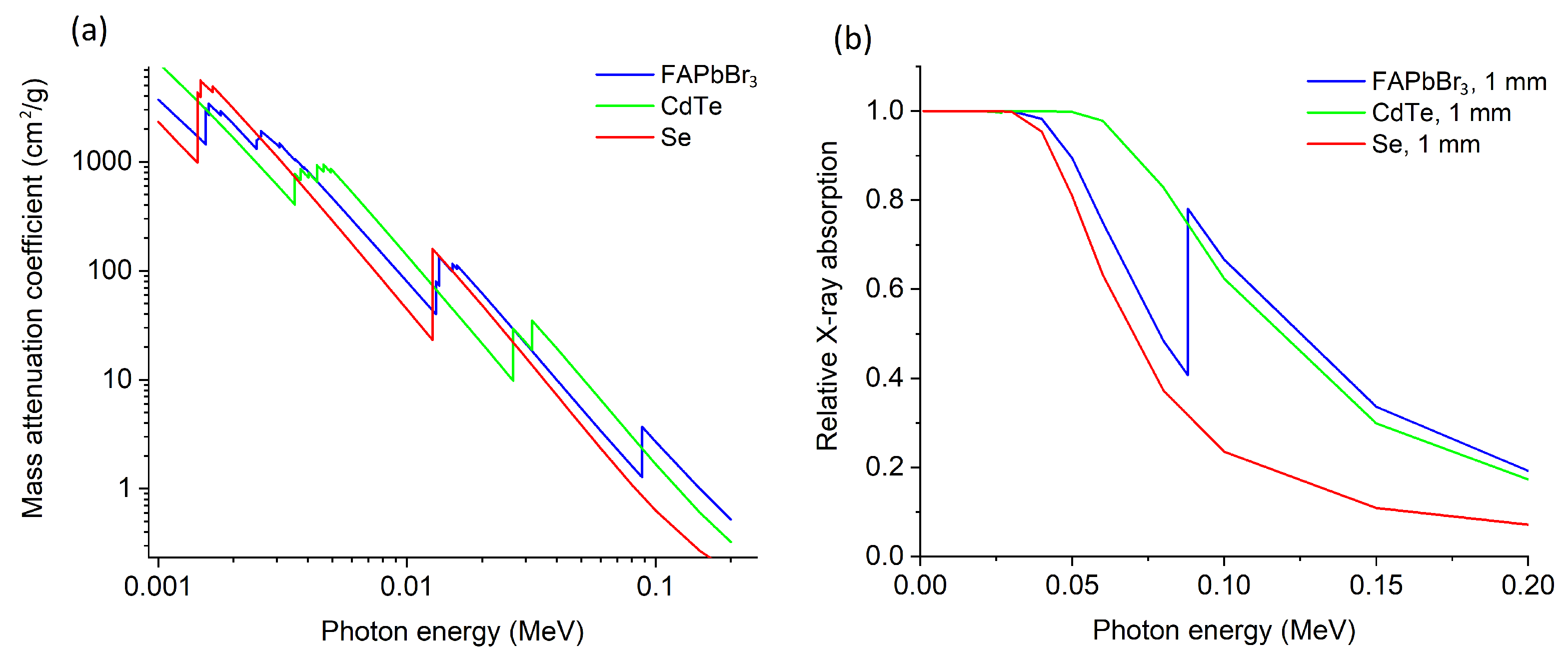
Figure 1a shows the calculated X-ray total mass attenuation coefficient as a function of X-ray energy for FAPbBr
, which is compared to that of two major detector materials cadmium telluride (CdTe) and selenium (Se), modelled using the NIST XCOM photon cross section database [
11]. The total mass attenuation coefficient of FAPbBr
has a broadly similar energy dependence to that of CdTe, although with some boost at higher energies above the lead K-shell absorption edge (e.g., at energies above 85 keV).
The relative X-ray absorption
for a detector of thickness
x is given by
where
is the mass attenuation coefficient of the detector material, and
is the material density (see
Supplementary Information and references [
12,
13,
14,
15]). Using Equation (
1),
Figure 1b compares the relative X-ray absorption for a 1mm thick detector of FAPbBr
with CdTe and Se, showing that FAPbBr
has a very similar detection efficiency to CdTe for energies above the Pb K-shell absorption edge. For X-ray energies below the K-shell edge, the relative X-ray absorption of FAPbBr
is slightly less than that of CdTe, i.e., approximately 20% less at 50 keV.
In photoconductive mode the X-ray sensitivity of the detector is determined by the magnitude of the photocurrent produced by the interaction of X-rays. The sensitivity is controlled by both the relative X-ray absorption and the charge transport performance of the detector material. In polycrystalline perovskite materials, the charge transport performance may be limited by the microstructure of the material, and also by the presence of grain boundaries (see
Supplementary Information). Previous reports by Shrestha et al describe large wafers of MAPbI
with a diameter of 1.27 cm and a thickness of 1 mm, produced by applying a pressure of 0.3 GPa to MAPbI
microcrystals. These devices showed a sensitivity of 2527 µC Gy
cm
under 70 kVp X-ray exposure [
16]. Yang et al. introduced a post-annealing process to passivate the ionic migration in pressed wafers of the ‘double perovskite’ Cs
AgBiBr
, which exhibited an X-ray sensitivity of 250 µC Gy
cm
[
17]. The same group have also reported the development of X-ray detectors using hot pressing of CsPbBr
to form a quasi-monocrystalline film at temperatures of up to 870
K [
18]. However, the fabrication of X-ray detectors using pressed polycrystalline FAPbBr
has not been reported so far.
We have grown micro-crystals of FAPbBr
by solution growth, using the inverse temperature crystallisation method (ITC) [
19]. The perovskite micro-crystals were used to fabricate a polycrystalline pellet for use as a X-ray detector. A hydraulic press provided pressures ranging from 12 to 124 MPa, and was used to synthesize the FAPbBr
micro-crystals into pellets of 10 mm in diameter, and with thicknesses between 1 mm and 2.5 mm. The pellets were annealed after pressing at 145
C for 15 min in air in order to optimise their conductivity and charge transport properties. Electrical contacts were deposited onto the top and bottom surfaces of each pellet using thermally-evaporated gold. A mechanical mask was used during the contact evaporation to produce circular gold contacts with a diameter of 4 mm. The optical properties of the pellets were studied using photoluminescence spectroscopy, and the morphology of the pellet structure was examined using scanning electron microscopy (SEM) and X-ray diffraction (XRD). The electrical properties and X-ray sensitivity of the devices were systematically studied using a 40 kV X-ray beam, and the effect of different pressures and annealing processes was examined.
2. Materials and Methods
Materials. FABr (98%) was purchased from Ossila Ltd, Sheffield, UK. PbBr (>99%), dimethylformamide (DMF, >99.8%) and gamma-butyrolactone (GBL, >99.9%) were purchased from Merck Life Science, Gillingham, UK.
FAPbBr polycrystals. FAPbBr polycrystals were grown using the inverse temperature crystallization method (ITC). Specifically, FABr (0.01 mol, 1.25 g) and PbBr (0.01 mol, 3.67 g) were added into 10 mL of DMF:GBL (1:1 v/v) within a glass flask. The temperature was increased gradually from room temperature 20 C to 80 C over the course of 24 h.
Pellet fabrication. FAPbBr polycrystals were ground by hand to achieve a uniform FAPbBr powder. A hydraulic press was then applied to make 0.3 g of the powder into a 1 cm diameter pellet with different pressures ranging from 12 MPa to 124 MPa.
SEM. The microstructure of the FAPbBr pellets was analyzed by imaging the fracture surface using scanning electron microscopy (SEM). A JEOL JSM-7100F Field Emisson SEM was operated at 15 kV, and a ThermoFisher Scientific Verios G4 Field Emission SEM was operated at 5 kV and 0.10 nA to collect secondary electron images.
AFM. AFM measurements were carried out using a Bruker Innova AFM.
Device fabrication. FAPbBr X-ray detectors were fabricated from a pressed pellet, with a [Au (90 nm)/FAPbBr pellet (2 mm)/Au (90 nm)] vertically-stacked structure. The Au electrodes were deposited using thermal evaporation.
Photoluminescence (PL) of FAPbBr pellets. PL was recorded using a continuous-wave green laser of 552 nm, with an optical power of 30 mW at room temperature. Optical spectra were acquired using a QE6500 spectrometer (Ocean Insight, Duiven, The Netherlands).
XRD. X-ray diffraction (XRD) patterns were collected using a Malvern Panalytical Empryean III X-ray diffractometer. The instrument was equipped with Cu K
radiation (
= 0.154 nm) and operated at 45 kV and 40 mA. The simulated diffraction pattern was obtained using the MDI Jade software package and atomic parameters from previously published results [
20].
X-ray and I–V measurements. Both dark current and X-ray photocurrent measurements were carried out using a Keithley 2400 source-meter (Tektronix UK Ltd, Bracknell, UK), with a programmable scan rate and settling time. For X-ray photocurrent and sensitivity measurements the device was irradiated with X-rays from an Amptek MiniX2 X-ray (Amptek, Bedford, USA [
21]) source with an Au anode and an acceleration voltage of 40 kVp (see
Supplementary Information). The sample was placed 45 mm away from the X-ray source. For the switched X-ray photocurrents, a mechanical tungsten X-ray chopper was used with a switching time of 5 ms.
3. Results and Discussion
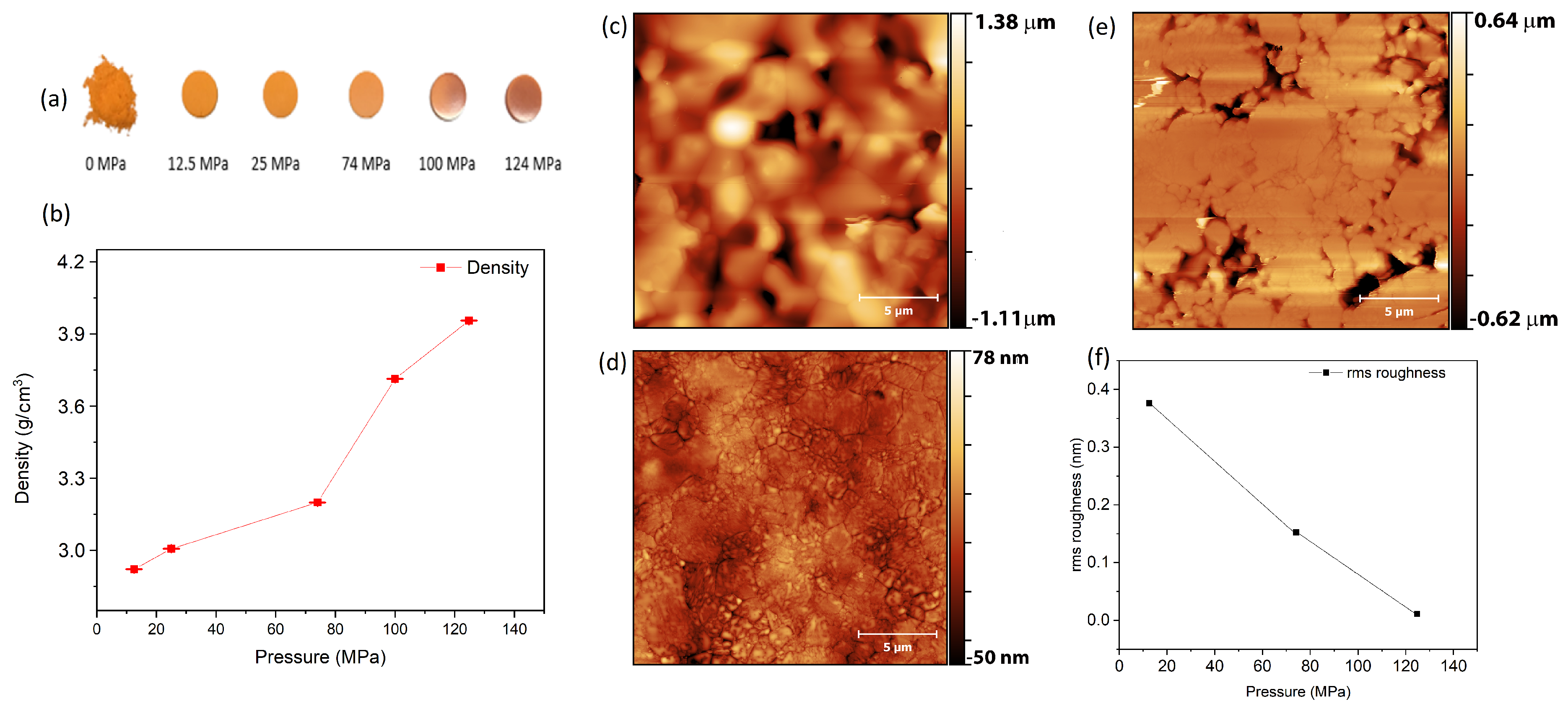
FAPbBr
pellets were fabricated with a diameter of 10 mm and with thicknesses in the range 1 mm–2.5 mm, using different applied pressures ranging from 12 to 124 MPa.
Figure 2a shows the slight variation in colour of the pellets from bright orange at lower pressures, becoming a darker orange with a mirror-like surface at pressures of 100 MPa and 124 MPa. The thickness of the pellets decreased slightly with increasing pressure and there was a commensurate increase in density of approximately 35% over the range of pressures (
Figure 2b). AFM topography imaging, shown in
Figure 2c–e, shows the impact of pressure on the surface topology and roughness of the FAPbBr
pellets. The root mean square (rms) roughness of the surface,
Figure 2f, reduces with increasing pressure to <20 nm at a pressure of 124 MPa, producing a smooth pellet surface.
3.1. Photoluminescence Studies
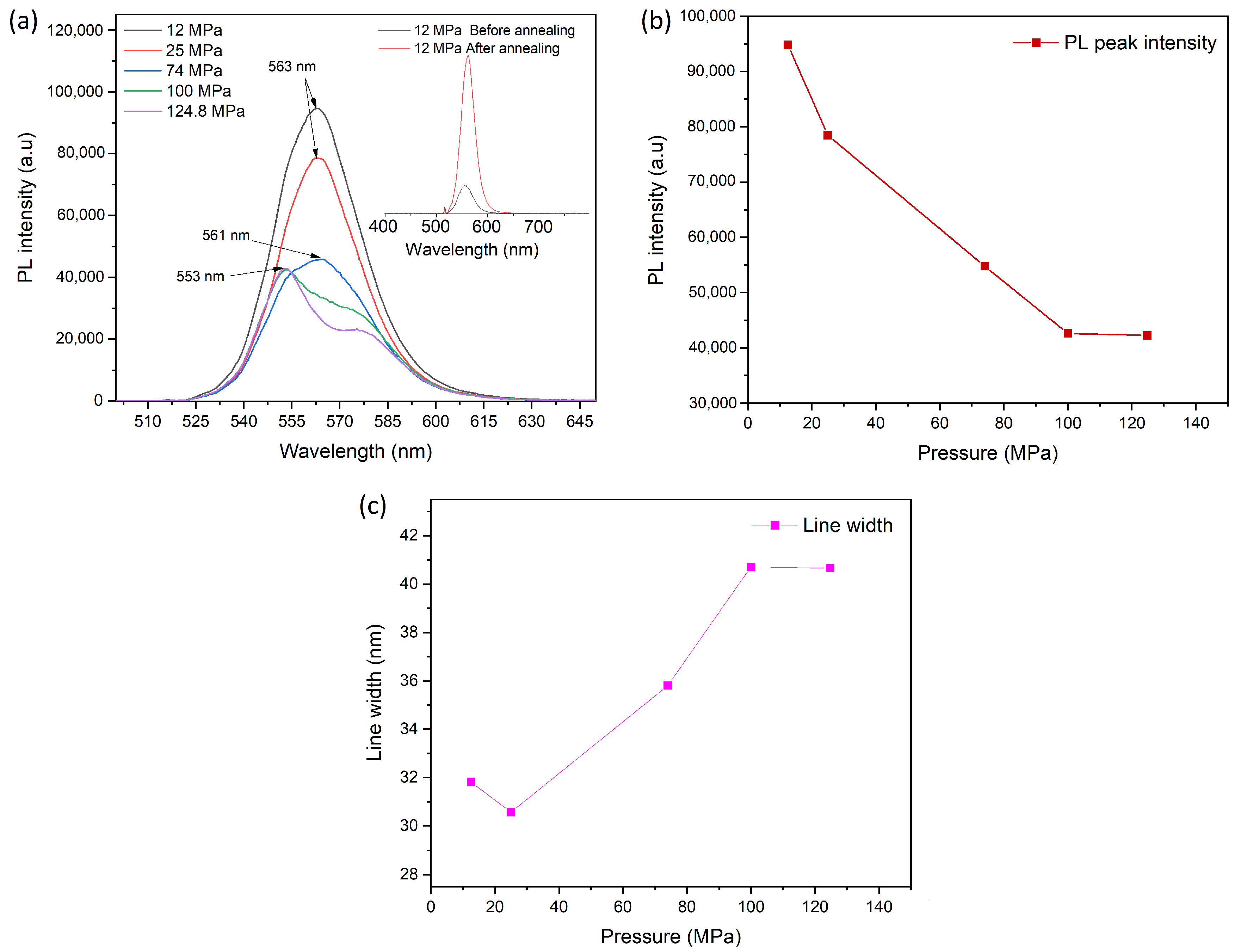
The PL behaviour of FAPbBr
pellets as a function of the pressure used during their fabrication were investigated by acquiring room temperature PL spectra of a set of five pellets. The PL measurement was carried out using a continuous-wave green laser with a wavelength of 520 nm. Each of the pellets was prepared under identical conditions, apart from the pressure used during pressing. The PL study shows three different aspects of the impact of pressure on FAPbBr
pellets in terms of changes of the peak intensity, peak line width, and bandgap evolution. As has been previously reported for organic lead halide perovskites, the near band-edge room temperature PL emission is extremely bright [
22], which was observed in our samples both for the as-grown crystals and for the pellet devices.
Figure 3a shows the broad emission with a peak emission wavelength at approximately 565 nm, consistent with the presence of the bromine halide anion.
Figure 3a,b show the decrease in PL intensity as a function of increasing pressure, indicating an increase in non-radiative processes in the near-surface region of the material since the penetration depth of the incident laser is <100 nm [
23]. For pellets formed at higher pressures the surfaces showed a mirror-like finish, consistent with a reduction in porosity and increased material density, which may also contribute to the reduced photoluminescence intensity.
The inset data in
Figure 3a shows the dramatic increase in PL intensity when the 12 MPa pellet was annealed at 145
C in the air for 15 min. All pellets showed a similar significant increase in PL intensity after annealing in air, which may be attributed to the presence of oxygen atoms during the annealing process acting as a passivator in perovskite materials. The role of oxygen passivation of surface defects in perovskites has been discussed by Lu et al. [
24] where O
atoms were found to passivate surface traps caused by lead dangling bonds which attenuated the non-radiative recombination rate and increased the PL intensity.
The corresponding linewidth of the PL spectrum was seen to widen by 25% with increasing pressure, as shown in
Figure 3c, due to the formation of a secondary PL peak at slightly shorter wavelength. Other studies of bandgap changes in lead halide perovskites have been reported, for example in CsPbBr
where the bandgap energy increased at very high pressures >1 GPa due to lattice amorphization [
25,
26]. Reports of high pressure studies of FAPbBr
nanoparticle showed phase transitions and changes in bandgap energies at pressures in the range 1–4 GPa [
27,
28,
29]. However these effects were observed at pressures significantly greater than those used in our study. We attribute the observed band gap increase in our samples to changes in microstructure as a function of increased pressure.
3.2. Microstructure and Surface Topology
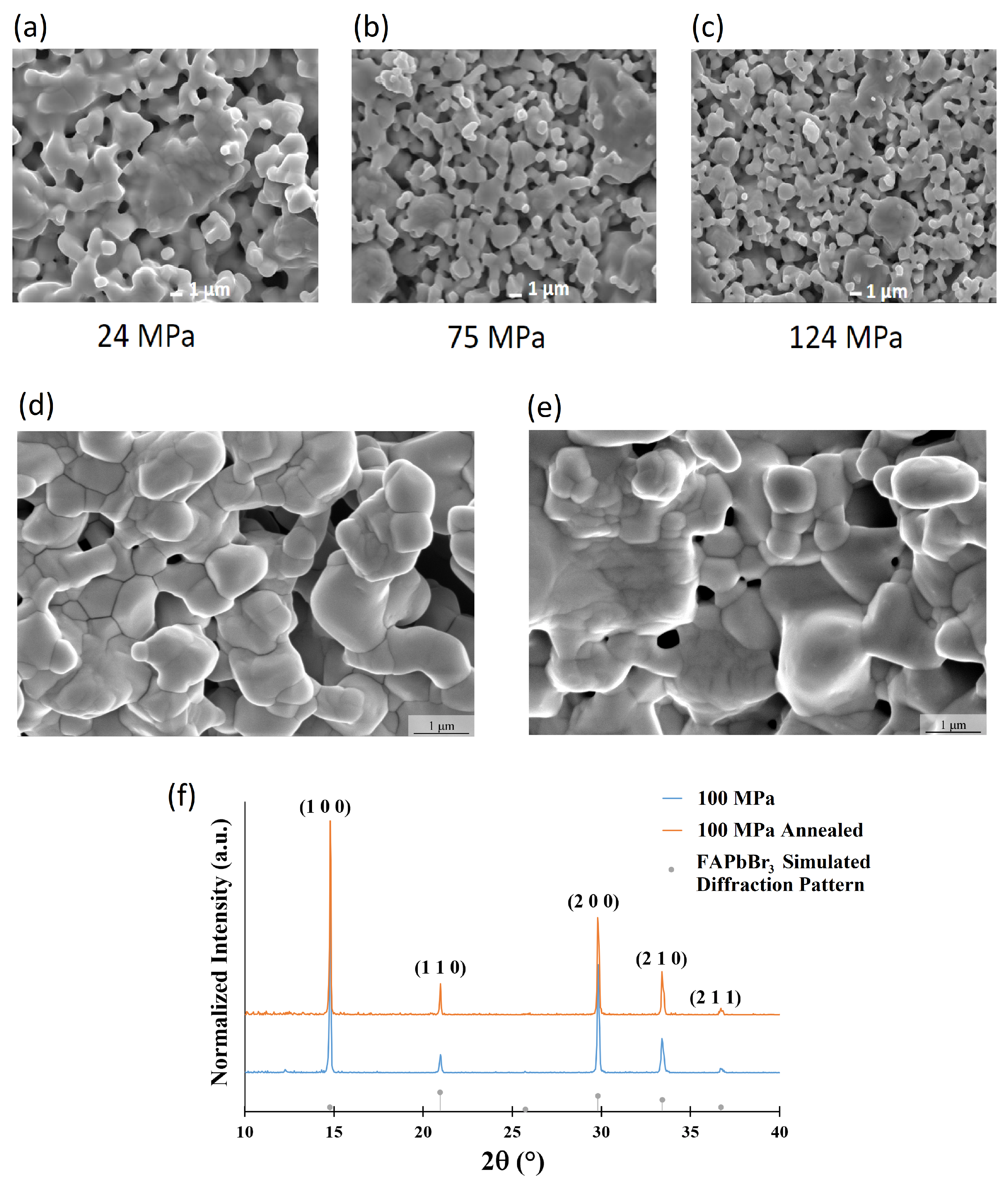
The top and cleaved surfaces of the pellets were imaged with SEM to examine the microstructural changes as a function of varying pressures and annealing conditions.
Figure 4a–c shows the evolution of the FAPbBr
pellet morphology as a function of different pressures. At the lowest pressure of 24 MPa the material shows a high degree of porosity, and also a large variation in grain sizes due to the manual process used to grind the as-grown crystals. As the pressure increases, the amount of porosity appears to decrease, which correlates with the measured increase in density. This reduction of porosity with increased pressure may be due to the annihilation of large particle agglomerates, additional compaction forcing grains closer together, and/or pressure induced sintering resulting in additional neck growth between individual particles.
Figure 4d,e are SEM micrographs of the pellet fracture surface comparing the microstructure of the pellet before and after annealing, with the pellets formed using a pressure of 100 MPa. The annealing process was carried out in ambient air, at a temperature of 145
C for 15 min. Annealing at these conditions successfully induced additional sintering and grain growth, with the grain size appearing to increase and the overall porosity decreasing.
XRD measurements, shown in
Figure 4f, were conducted on an annealed and a non-annealed pellet pressed at the same 100 MPa pressure and compared to a simulated XRD pattern. No significant differences in peak position or overall phase were observed comparing the two samples, suggesting that the phase and stress state of the pellet did not change due to annealing. Compared to the simulated diffraction pattern [
20], the pellets pressed at 100 MPa before and after annealing have preferred orientation along the (1 0 0) family of planes. This preferred orientation may be associated with the anisotropic pressing process used to consolidate the powder into pellets. Also, the orientation of the FA molecule within the cubic FAPbBr
crystal structure may not be uniform throughout the sintered pellet. As a result, the simulation may not demonstrate a representative distribution of FA molecule orientations, which may impact the overall structure factor of the crystal and subsequent observed diffraction intensities. The FWHM of the diffraction peaks narrowed after annealing, suggesting an increase in crystallite size. This is consistent with the observed changes in microstructure seen in the fracture surface SEM.
3.3. Electrical Resistivity
FAPbBr
X-ray detectors were fabricated by thermally-evaporating 90 nm thick gold contacts onto both sides of each pellet, and their charge carrier transport properties and X-ray sensitivity were investigated. The conductivity of the resulting ’sandwich’ device structure of [Au/FAPbBr
/Au] was measured in terms of dark current density as a function of applied bias voltage, and showed an ohmic response which was symmetric for either voltage polarity.
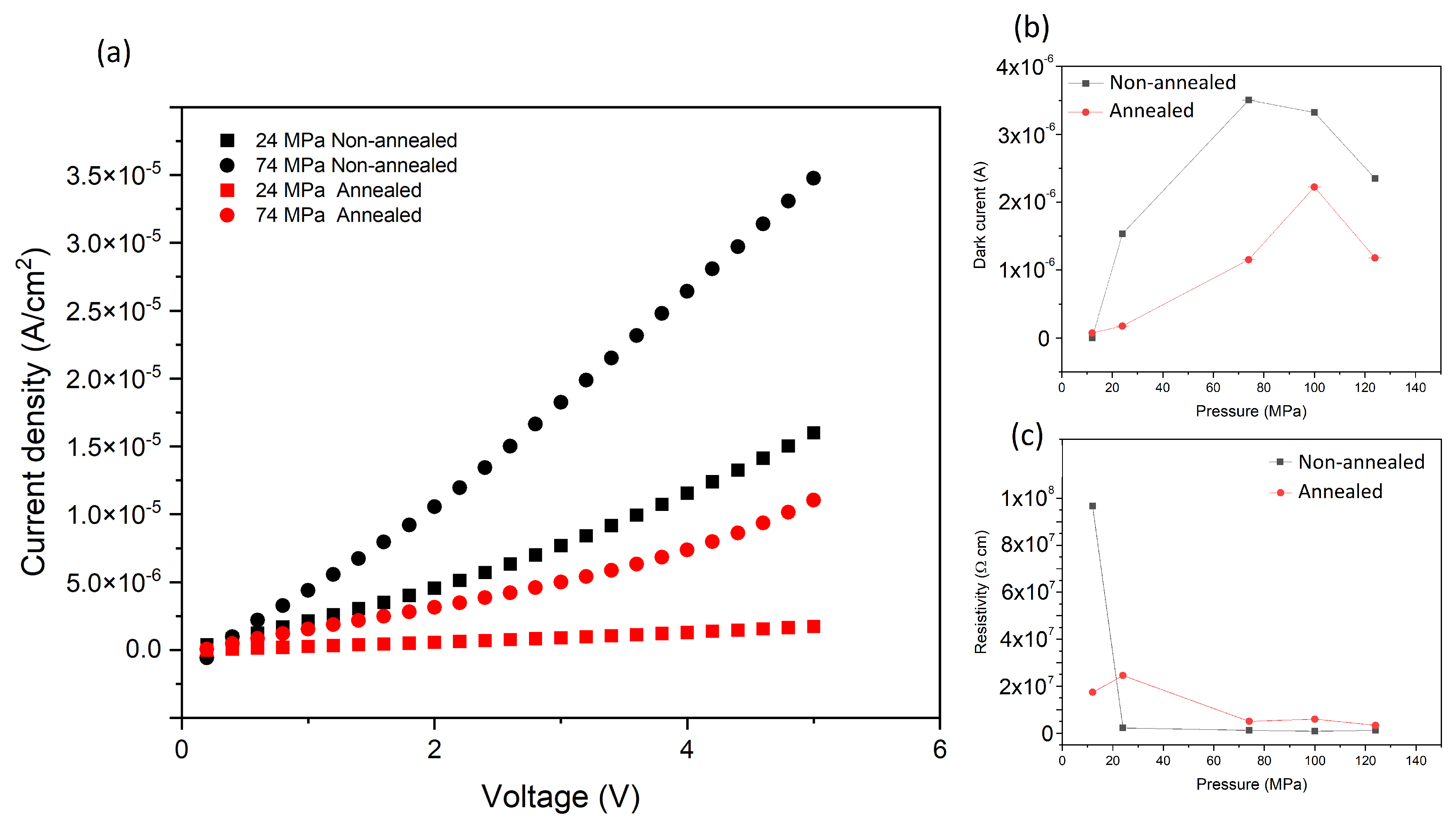
Figure 5a shows the dark current density for pellets which were formed at 24 and 74 MPa, both with and without the annealing process. In general the current density for the 74 MPa pellet was higher than that of the 24 MPa pellet, indicating improved conductivity when the material is pressed at the higher pressure.
Figure 5b shows the overall trend of dark current, measured at 5 V, across the full pressure range. Both figures also indicate the effect of pellet annealing, which generally shows a reduction of 2–3 times in dark current compared to the equivalent non-annealed pellet. This may indicate a reduction in active defects in the material after the annealing process.
The resistivity of the pellets was calculated by applying a linear fit to the dark current at low bias voltage. As shown in
Figure 5c the resistivity of the non-annealed devices was higher for the 12 MPa device, but dropped significantly for higher pressures, which is consistent with an increase in material density and improved conductivity. A similar trend was also observed for the annealed devices as the pressure was increased.
3.4. X-ray Sensitivity
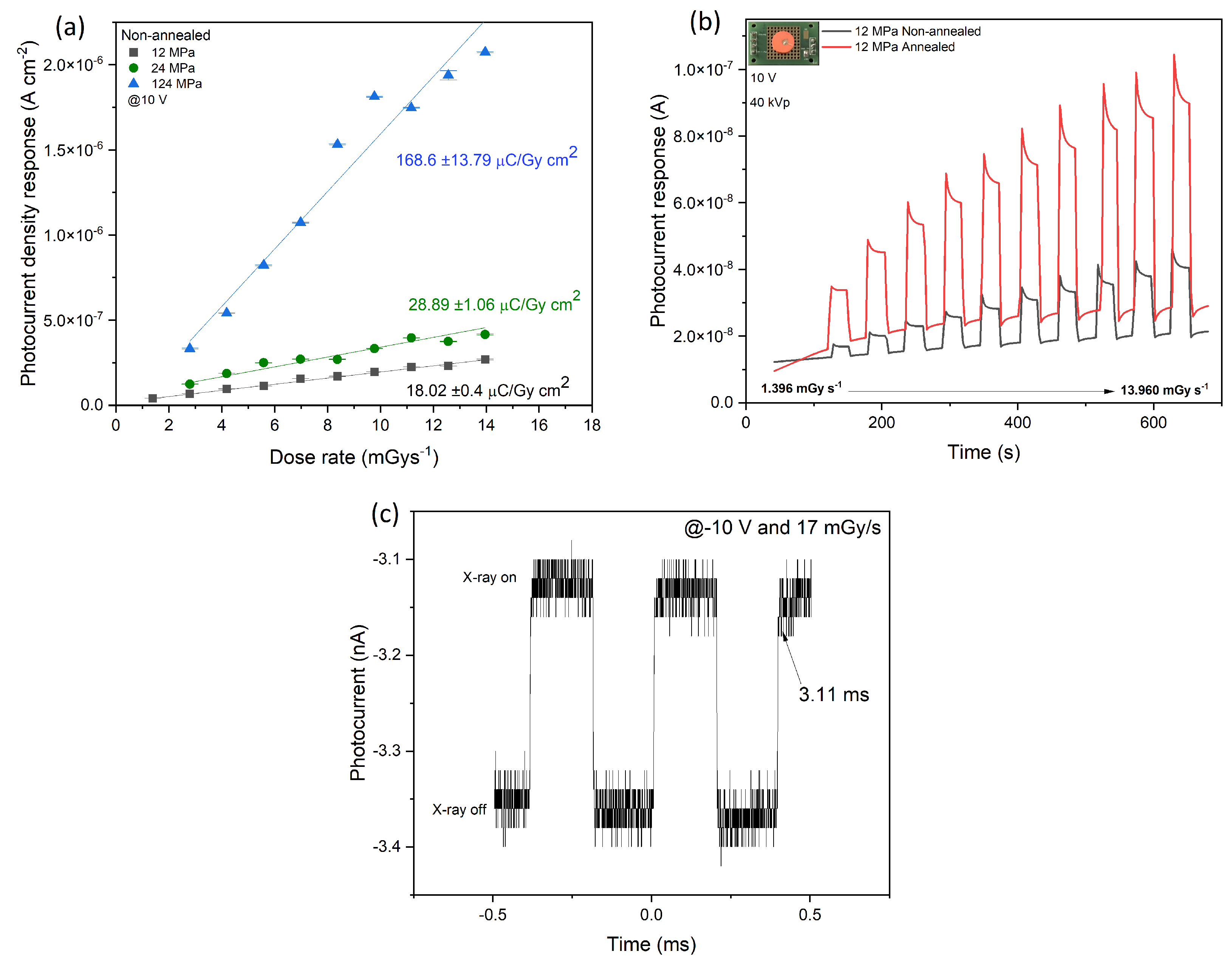
In order to assess the X-ray sensitivity and performance of the pellet devices, the samples were irradiated with a 40 kVp X-ray beam, where the beam current was controlled to vary the dose rate (air equivalent) from 1.4 to 14.0 mGy s. The radiation dose rate on the samples was calibrated using an ionisation chamber. The devices’ response was demonstrated by turning the incident X-ray on and off with various dose rates. The X-ray sensitivity of the device was calculated from the gradient of the photocurrent density as a function of dose rate.
Figure 6a shows the measured X-ray photocurrent as a function of increasing dose rate for a set of three FAPbBr
pellets produced with increasing pressure. The devices’ X-ray sensitivity shows a significant increase as the forming pressure is increased, with the sensitivity at 10 V bias increasing from 18.0 µC Gy
cm
for the 12 MPa pellet, to 168.6 µC Gy
cm
for the 124 MPa pellet. Although there is a small increase in pellet density as the pressure is increased, shown by
Figure 2b, any resulting increase in the X-ray absorption efficiency is not the dominant cause of the higher detector sensitivity. In fact, these results confirm that the increased X-ray sensitivity is predominantly due to the improved charge transport properties of the material formed at higher pressures caused by the observed changes in microstructure of increased grain size and decreased porosity.
The influence of post-processing annealing of the pellets on X-ray sensitivity was also studied, with the annealing carried out on pellets at 145
C in ambient air for 15 min.
Figure 6b shows the increase is X-ray photocurrent due to annealing for a pair of pellets that were formed with a pressure of 12 MPa. The annealed device showed a significant increase in X-ray sensitivity to 46.6 µC Gy
cm
, compared to the 12 MPa non-annealed pellet. All the pellets formed at different pressures showed increased sensitivity after annealing (see
Supplementary Information), although the relative improvement was much less significant for those pellets formed at higher pressure. The observed improvement in X-ray sensitivity after annealing is again consistent with improved charge transport due to the increase in grain sizes and improved microstructure within the material.
The X-ray response time was measured for the 75 MPa FAPbBr
annealed pellet using a 10 V bias voltage, with a mechanically-chopped X-ray beam with a dose rate of 17 mGy s
.
Figure 6c shows the resulting photocurrent signal which has an on/off response time of 3.1 ms, which is limited by the speed of the mechanical shutter. Therefore the response speed of the perovskite detector is faster than our instrument limit.
This work has demonstrated the X-ray detection performance of polycrystalline pressed FAPbBr
pellets as X-ray detectors, achieving a maximum sensitivity of 169 µC Gy
cm
at 40 keV for a device with a thickness of 2 mm. This measured X-ray sensitivity is 8 times greater than typical values for a 200
m thick amorphous selenium X-ray detector [
30], and comparable with the sensitivity of a 350
m thick polycrystalline CZT X-ray detector [
31].
Table 1 summarises the X-ray sensitivity of other recently reported perovskite X-ray detectors, for example polycrystalline pellets of the double perovskite Cs
AgBiBr
which achieved an X-ray sensitivity of 250 µC Gy
cm
[
17]. Higher sensitivities of up to 2500 µC Gy
cm
were reported by Shrestha et al. [
16] using the related organic lead halide perovskite MAPbI
, pressed at high pressures of up to 0.3 GPa.


 ,
, 


