Article

Method to Predict Performances of PCB Silicone Conformal Coating under Thermal Aging

1
Dow (Shanghai) Holding Co. Ltd., Shanghai 201203, China
2
Dow Silicones Belgium SRL., B7180 Seneffe, Belgium
*
Author to whom correspondence should be addressed.
Appl. Sci. 2022, 12(21), 11268; https://doi.org/10.3390/app122111268
Submission received: 6 September 2022 / Revised: 30 October 2022 / Accepted: 2 November 2022 / Published: 7 November 2022

Abstract

:

Featured Application

Silicone conformal coating for PCB protection in the electronic industry.

Abstract

The stability of print circuit board (PCB) conformal coating is critical to guarantee the long-term performance of electronic components on PCB boards. Coating exposure to thermal shock or temperature cycles may initiate cracks, a common failure mechanism of conformal coatings. Different simplified approaches are compared to help identify desired mechanical profiles for coatings to be used in a harsh environment, focusing on silicone characterized by low rigidity and high deformability compared to alternative chemistries. Evaluation of the bi-material strip bending test method appears not to be effective in the conformal coating selection. The large difference between the coating’s elastic modulus of silicones compared to substrate modulus allows the use of a simplified formula to calculate the stress associated with the coefficient of thermal expansion (CTE) mismatch, the silicone accommodating displacement imposed by thermal changes. Both lateral tensile stress and local shear stress near the edge are estimated, with local shear stress decreasing quickly and moving apart from the edge with the stress relaxation preventing coating delamination. Predictions of simplified models agree with both results of grid-independent finite element analysis (FEA) models and observations of test pieces submitted to temperature cycles. This demonstrates the ability to use simplified models to predict coating’s performances under thermal aging and help in product selection depending on the working environment.

1. Introduction

In recent years, electronics have played an increasing role thanks to digitization and artificial intelligence megatrends in both consumer and industrial applications. In applications like automotive and aerospace, electronics are exposed to harsh environmental conditions like high or low temperatures cycling, high or low pressures, radiations, corrosive surroundings like moisture, chemicals, and mechanical stresses like vibrations [1]. Therefore, there are increasing demands for reliable electronics operating in harsh environmental conditions along all device service life.
Conformal coating, a thin protective polymeric film that conforms to the contours of Printed Circuit Boards (PCB) and electronic components acts as a physical barrier against various environmental, mechanical, electrical, and chemical effects [2,3,4,5,6]. Five main families of conformal coatings exist on the market that differ by their chemistry (molecular structure, polymer backbone) and their physical properties [7]. They include silicone, acrylic, polyurethane, epoxy, and para-xylene. Amongst those, silicones, the most used technology, are synthetic polymers consisting of a silicon-oxygen backbone with organic groups attached to the silicon atoms. Silicone conformal coatings are very flexible, provide good adhesion, and are stable over a wide range of temperatures from −55 to +200 °C [8].
One of the characteristics of silicones is their large coefficient of thermal expansion (CTE), which is very different from the CTE of the PCB, electronic components, and solder joints. [2,3,9,10,11]. Most PCBs have a CTE lower than 20 ppm/°C [3,9,10,11], and most solder joints have a CTE lower than 25 ppm/°C [10,11], while silicone conformal coatings have CTE values above 200 ppm/°C [3]. This large CTE mismatch generates stress on the PCB, solder joints, and conformal coating layer, especially when the electronic device is subject to temperature variation during its service life, experiencing many electrical power on/off cycles. The accumulation of thermal and mechanical stresses can initiate surface fractures that may expand to deep section cracks [9,12,13]. The risk of device failure can result from crack initiation and propagation because creating an entry door for contaminants and moisture to go through the protective layer degrades the components and electrical connections. Pippola et al. [3,9] have studied conformal coatings of electronics under thermal shock test conditions. They used polyurethane or silicone as a casting material and silicone as a conformal coating material to apply on PCB to observe cycles to failure under thermal shock. It was found that conformal coating materials have a critical impact on the reliability of the electronic device. A study by Abbas et al. [2] found there is a strong relation between conformal coating thickness and electronic module failures under thermal cycling aging.
Stress in polymer coating has created enormous interest for many years [14,15]. One common method to simulate coating stress is to measure the curvature or deflection of a coated substrate through a bi-material strip bending (BMSB) experiment [16,17]. The BMSB method presents the advantage of not requiring a precise determination of the mechanical properties of polymeric coating, parameters that are complex to accurately measure on very rigid material. Finite element analysis (FEA) has been widely used to study the spatial distribution of local stress in polymer coatings resulting from external constraints [10,18,19]. For example, Lownders et al. [10] take an FEA study to predict that thermal stress may cause cracks in acrylic conformal coating at the edge of components attached to the PCB. Cracks appear when local stress calculated by FEA exceeds the threshold of material failure [14,20,21].
Though stress build-up in polymeric coatings has been extensively studied, there is no systematic study of crack appearance in silicone conformal coatings used for PCB protection that combines simplified model approach evaluation with FEA and experimental validation. In this work, two approaches are studied, and their capability to predict the suitability of a silicone coating to be used in conformal coating application is assessed. Approach 1 is the BMSB method for material assessment. Approach 2 is simplified equations of stress build-up in a bi-layer plate resulting from CTE mismatch obtained assuming plane stress approximation. Stress values calculated this way are validated by comparing FEA solutions of continuous mechanics equations and experimental observations. A rigid and a soft silicone conformal coating were used to test the above methods, aiming to determine the best performing product for each conformal coating application that differ regarding their service conditions and the range of temperature exposure.

2. Materials and Methods

2.1. Conformal Coating Material Selection

Two commercial silicone conformal coatings from Dow (named coating A and B) were selected to study the appearance of crack defects when PCB boards protected by those coatings are submitted to external stresses. Coatings were selected to be very different by intention regarding CTE values and mechanical properties (Table 1). Conformal coating A is harder, with higher scratch resistance benefits when handling PCB. Conformal coating B is softer with lower modulus and better deformability.

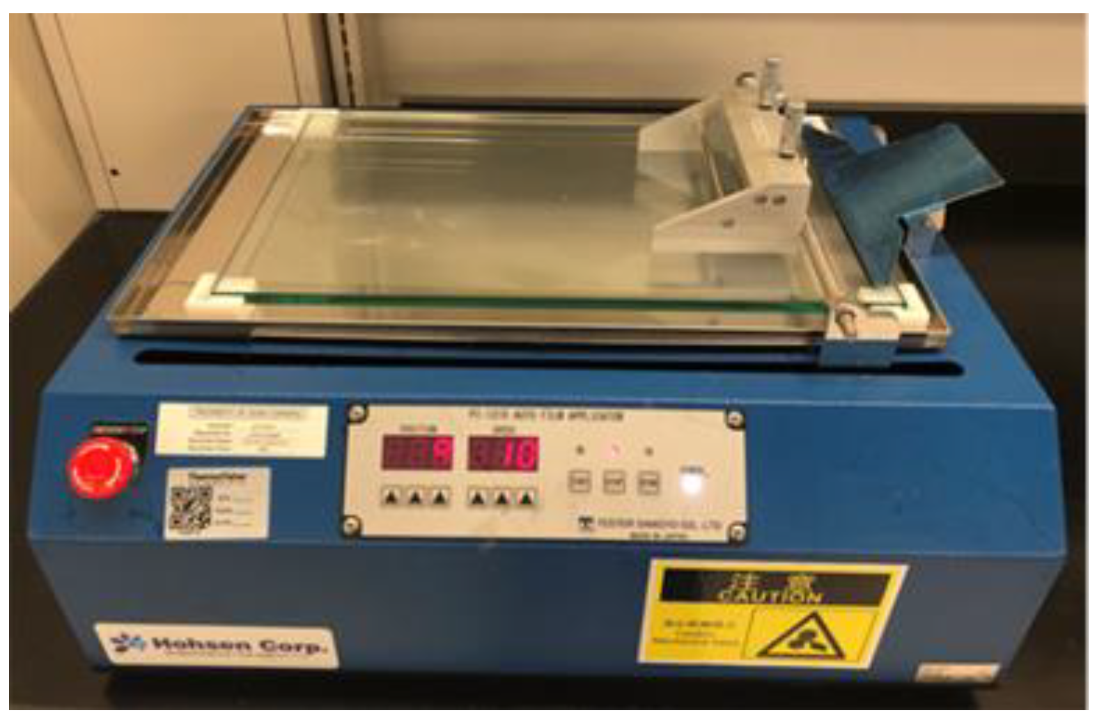
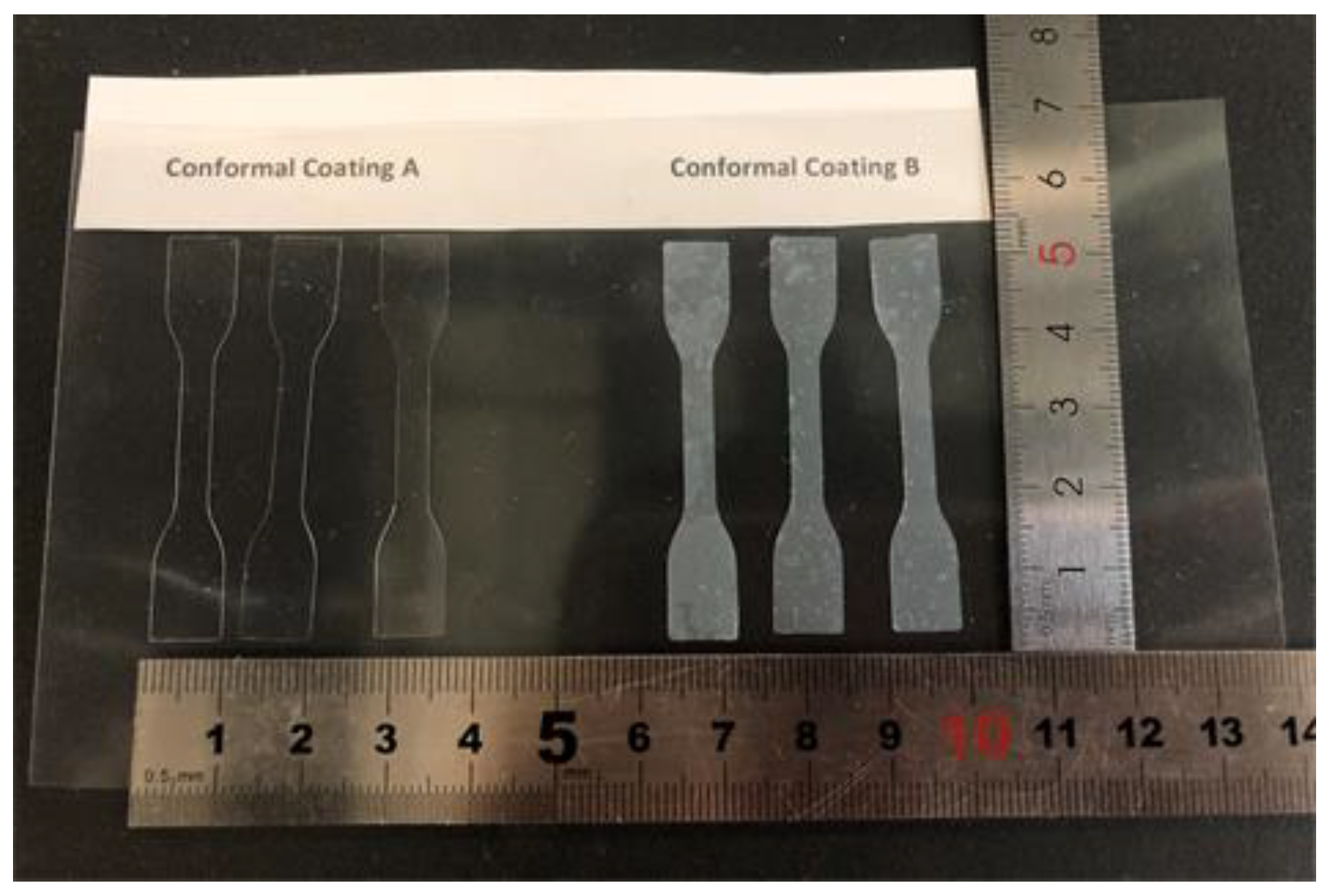
2.2. Conformal Coating Sample Preparation

Silicone conformal coating films A and B are coated using a Hohsen PI-1210 auto film applicator of 10 μm accuracy on a PET release liner (Figure 1). Meanwhile, both conformal coatings are spray-coated on a PCB using a PVA 350 benchtop coating system. Conformal coating thickness after drying is controlled to range from 100–120 μm. PCB used in this paper is from Hytera with XY-direction CTE equal to 18 ppm/°C.

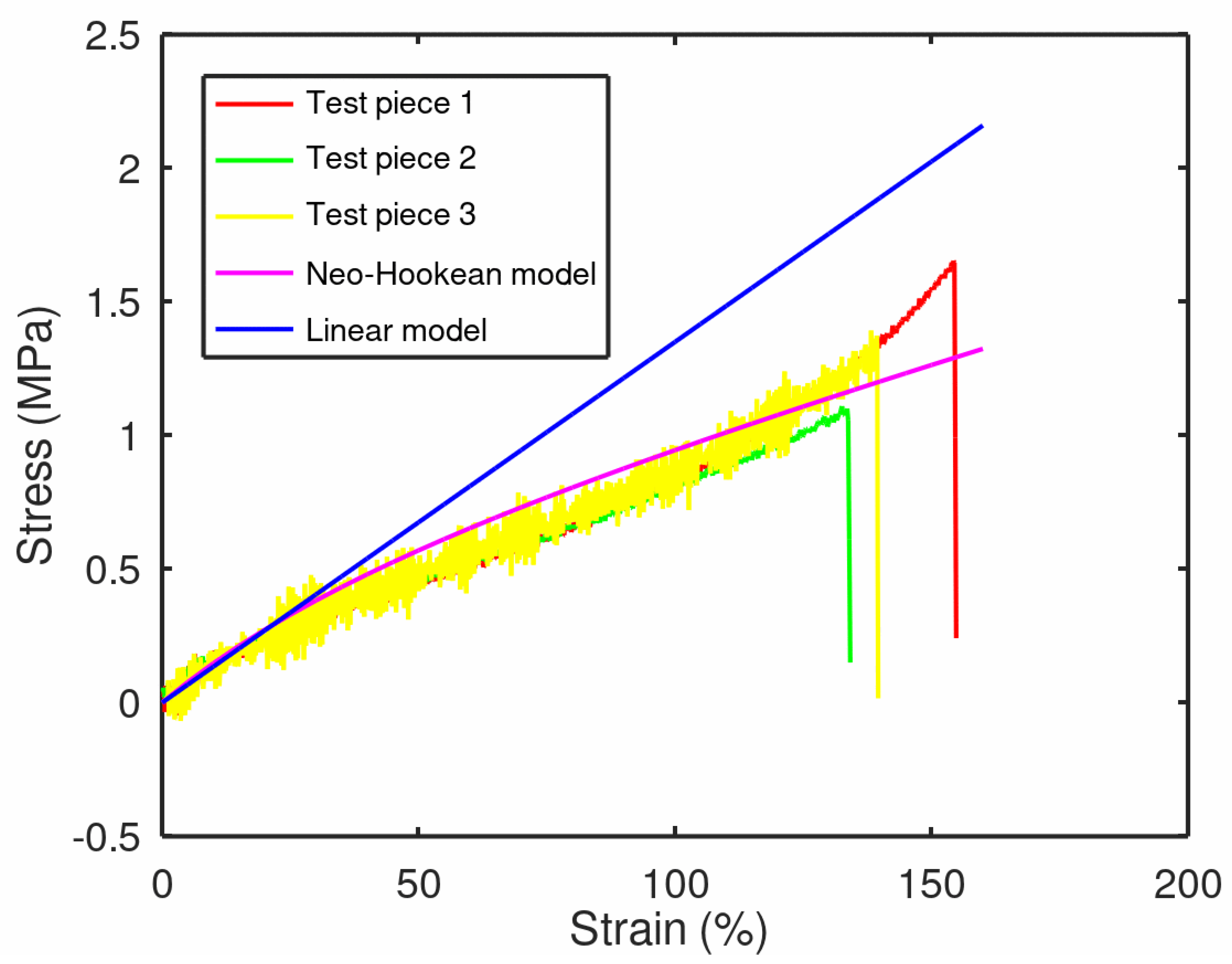
2.3. Tensile and Elongation Test

Conformal coating tensile and elongation properties are measured using a TA Texture Analyzer with a tensile fixture. Dog bone tensile sample geometry follows ISO 37 type 3 standard dumbbell test pieces with an overall length of 50 mm (Figure 2).

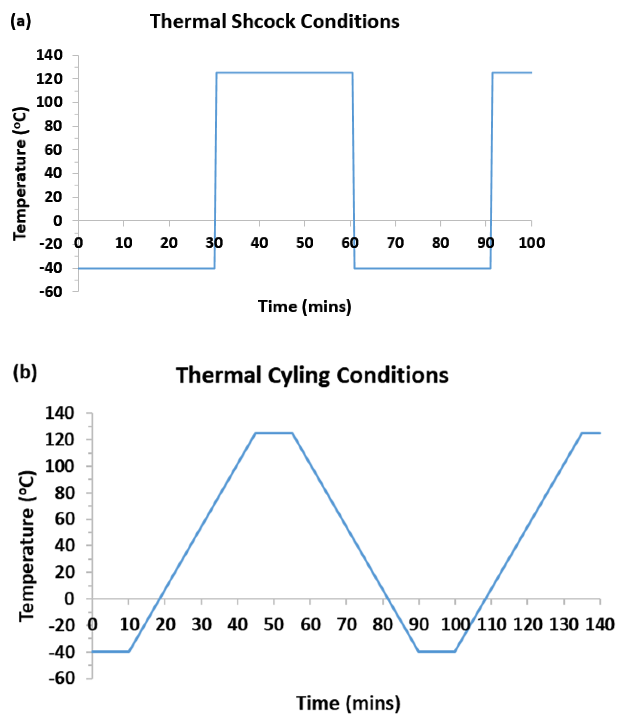
2.4. Thermal Shock and Thermal Cycling
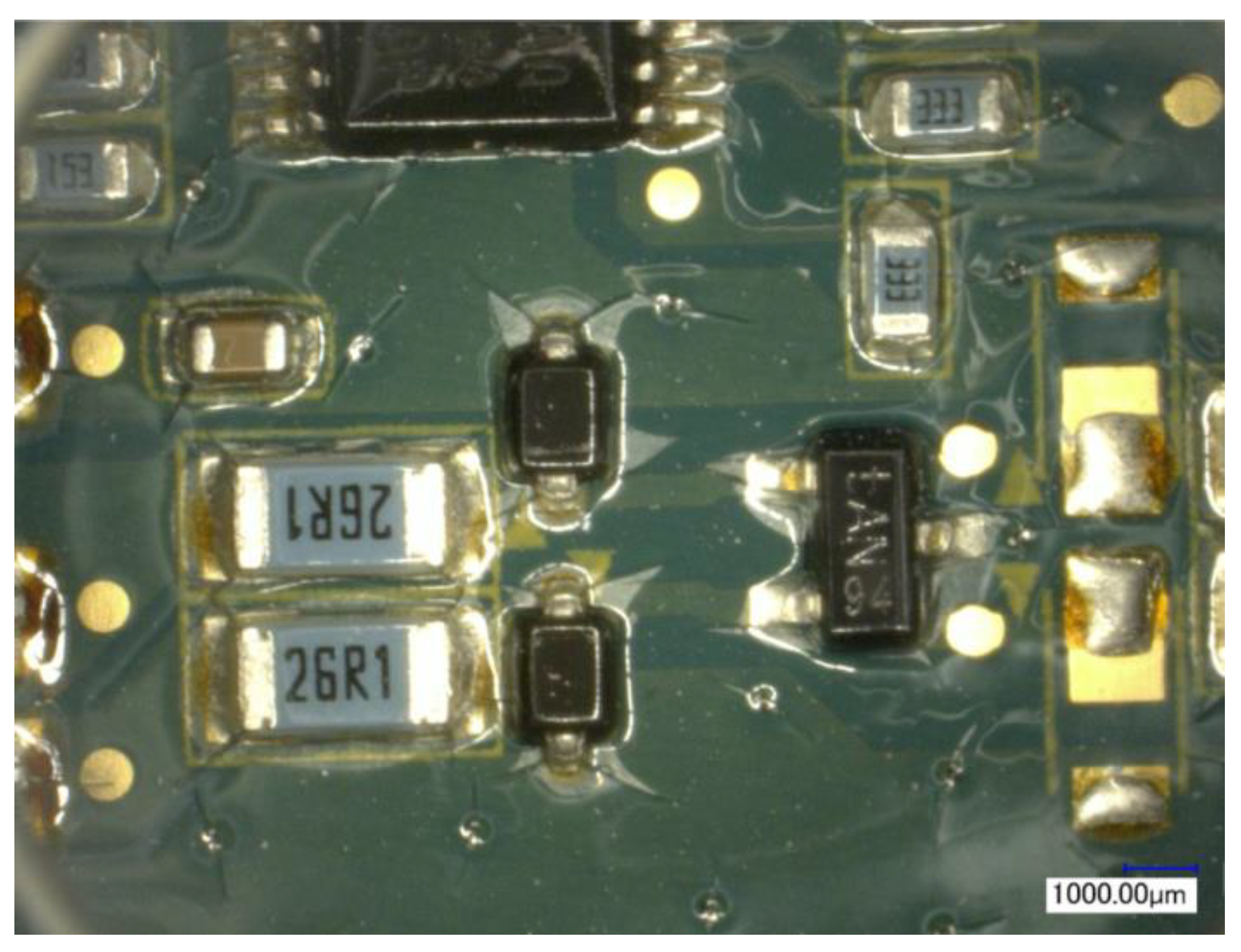
Silicone-coated PCBs are laid in an ESPEC TSE-11A environmental chamber for thermal shock aging and in an ESPEC EGNX 12-6 CWL environmental chamber for thermal cycling aging. Thermal shock aging conditions are −40 to +125 °C temperature exposure with a 30 min plateau at both −40 °C and +125 °C (Figure 3a). Temperature change from 40 °C to +125 °C is completed within 1 min. Thermal cycling aging conditions correspond to temperature cycles between −40 to +125 °C, with a 90 min cycle duration (Figure 3b). Dwell time at both −40 °C and +125 °C is 10 min.

2.5. Microscope

Camera and Keyence VHX-S50 digital microscope were used for PCB conformal coating cracks observation.

3. Results

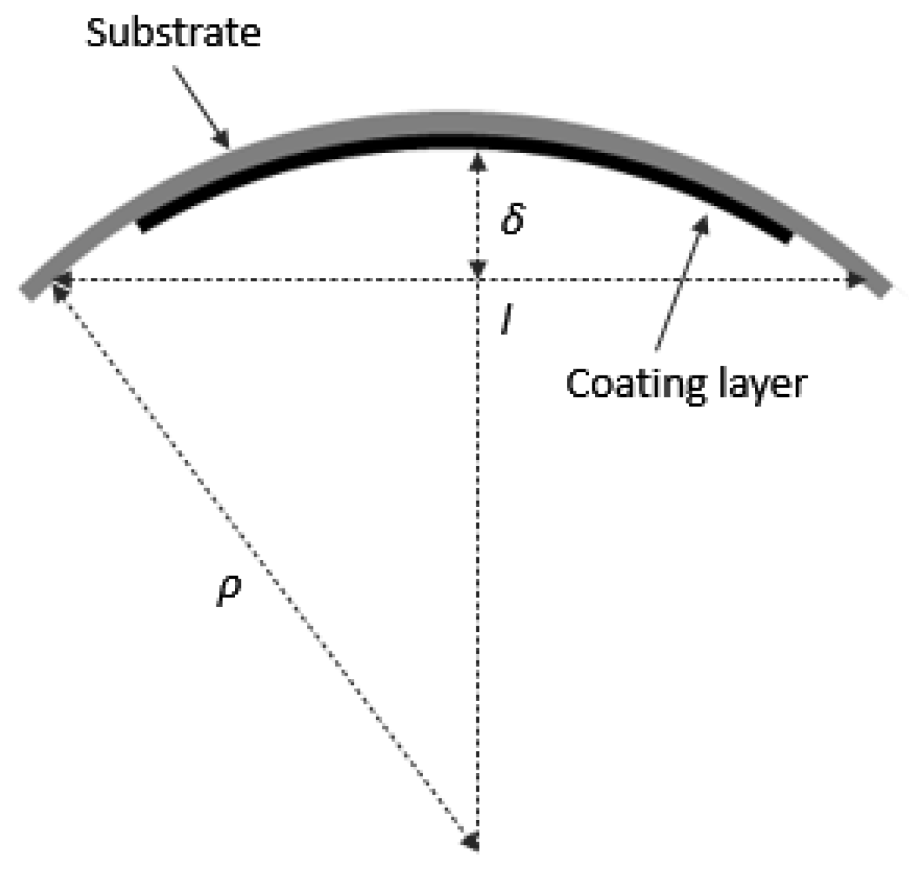
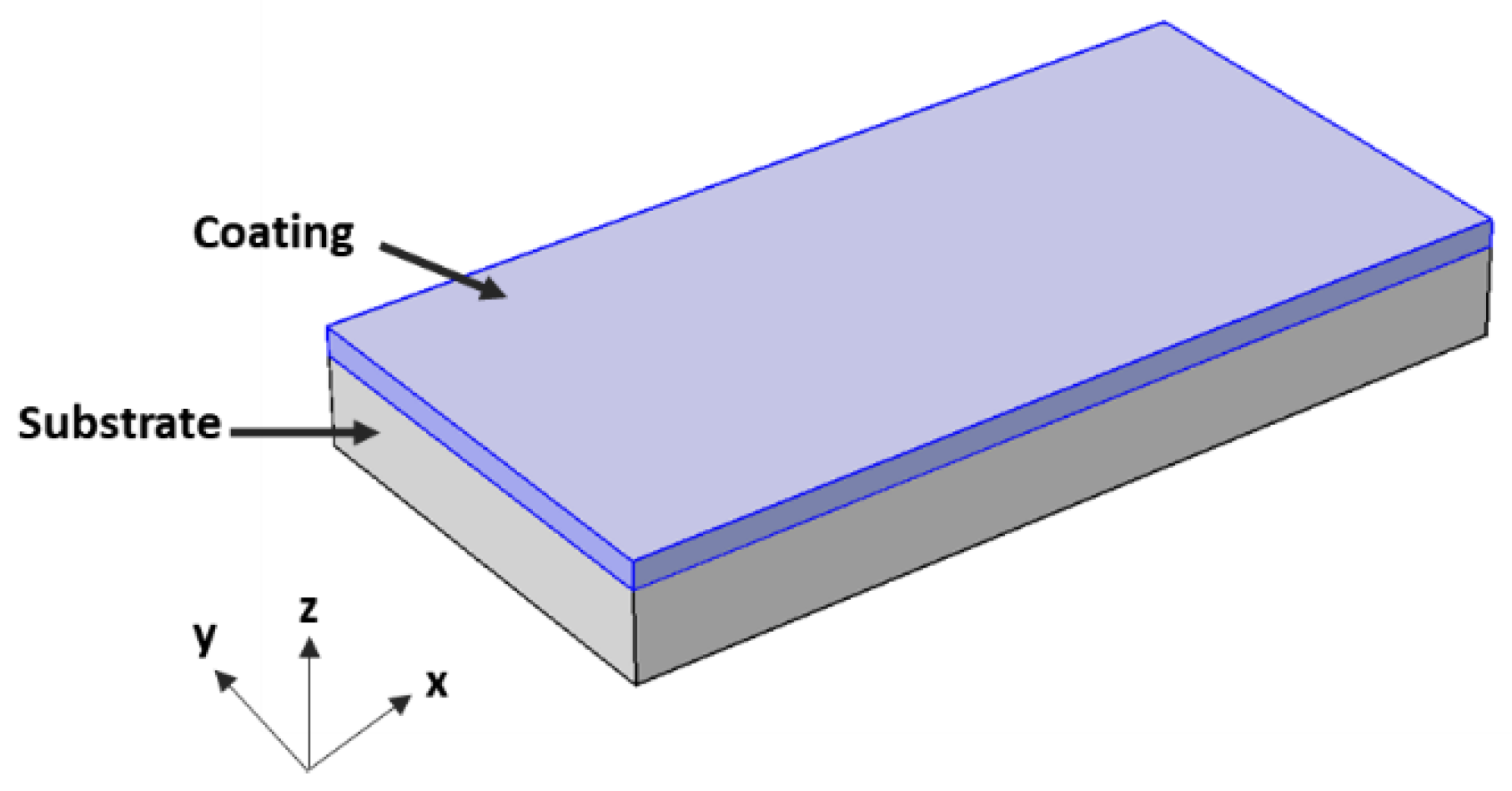
3.1. Bi-Material Strip Bending (BMSB) Characterization and Modeling

One well-known method to test the mechanical behavior of a substrate-coating assembly is to impose a deflection to a bi-layer strip set on two free rotation supporting points and to apply a force at an equal distance from each support to force bending of the strip. The well-known beam bending theory applied to a bi-layer material is used to calculate the residual stress in the coating [16,17]. Figure 4 shows the typical BMBS test.
When both coating thickness and the elastic modulus of the coating are small compared to corresponding values associated with the substrate, the relationship between the residual stress and beam deflection highly simplifies. In applications of the conformal coating protection of PCBs, those conditions are always satisfied because the coating thickness is much less than PCB thickness. In addition, compared to alternative conformal coating technologies, silicone materials are soft, with Young’s modulus of the coating being much less than Young’s modulus substrate. The assumption of the ratio of Young’s modulus of coating to the substrate’s modulus to be small is satisfied in most cases. With these assumptions, the equation between the residual stress and the deformation takes the following form:
σ a = 4 3   E s h s 2 h a l 2   δ
Equation (1) predicts that both high substrate Young’s modulus E s and high substrate thickness h s contribute to higher stress in the coating for any imposed displacement δ . On the contrary, higher coating layer thickness h a and span length l both lead to lower coating stress. It must be recalled that Equation (1) calculates the stress associated with a forced plate bending, i.e., the stress created in the coating layer results from an imposed curvature. In the present application, the bending comes from the difference in thermal expansion between the two components of the bi-layer material. However, because of the large difference in Young’s modulus between the substrate and the coating, as well as their different thicknesses, the CTE mismatch will not lead to any significant bending of the bi-material panel; the bi-layer panel stays undeformed, while the major fraction of differential displacement is absorbed by the deformation of the softer material, in our case, the silicone coating. In this case, the local stress built-up inside the coating must be dependent on Young’s modulus of the coating, a variable not appearing in Equation (1). For this reason, this method is not appropriate for silicone conformal coating evaluation.

3.2. Modelling Stress Build-up Associated with CTE Mismatch during Thermal Cycle Aging

The large CTE mismatch between silicone coatings and electronics components requires the accurate calculation of stress at equilibrium at both low and high temperatures, the change in temperature concerning the temperature of coating application creating either a negative or positive lateral differential displacement. The state-of-the-art method consists in solving solid mechanics equations using an FEA tool. However, this method is not necessarily the most appropriate for a first material selection because:
  • FEA modeling requires an accurate identification of the material elastic model: most silicone materials show a stress-strain nonlinear dependence, requiring multiple test piece geometries (uniaxial testing, pure shear, bi-axial testing) to accurately describe mechanical behavior, particularly when having stress-strain dependence showing saddle point that requires high order nonlinear models. Those measurements are particularly complex with very rigid material, having low deformation capabilities;
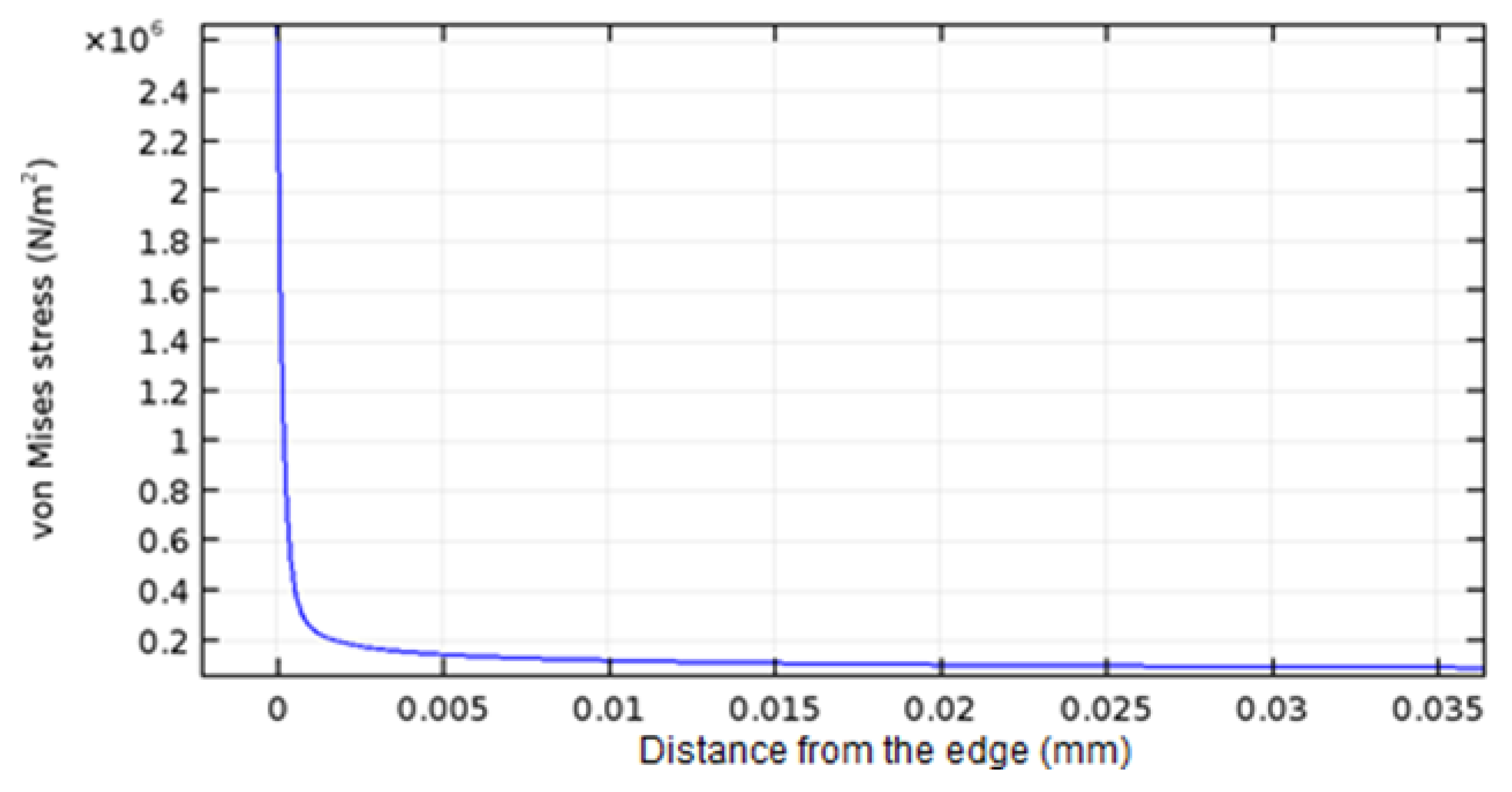
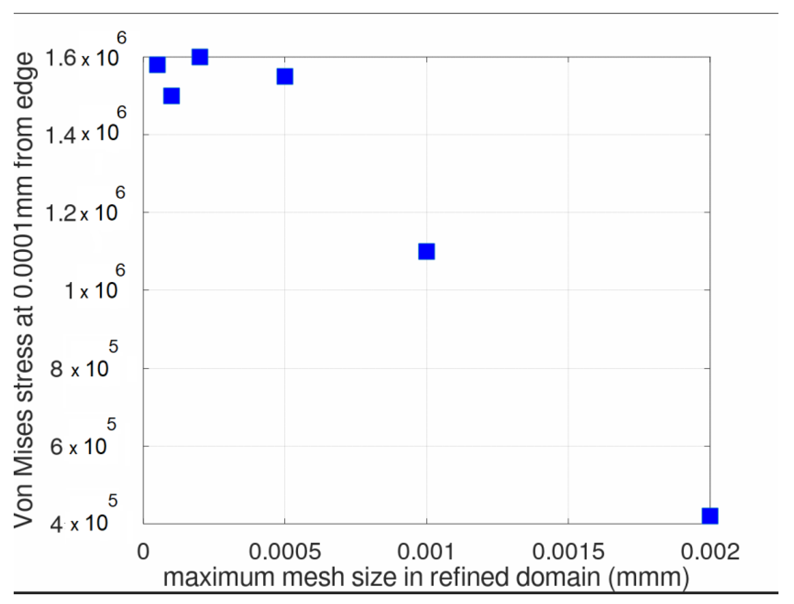
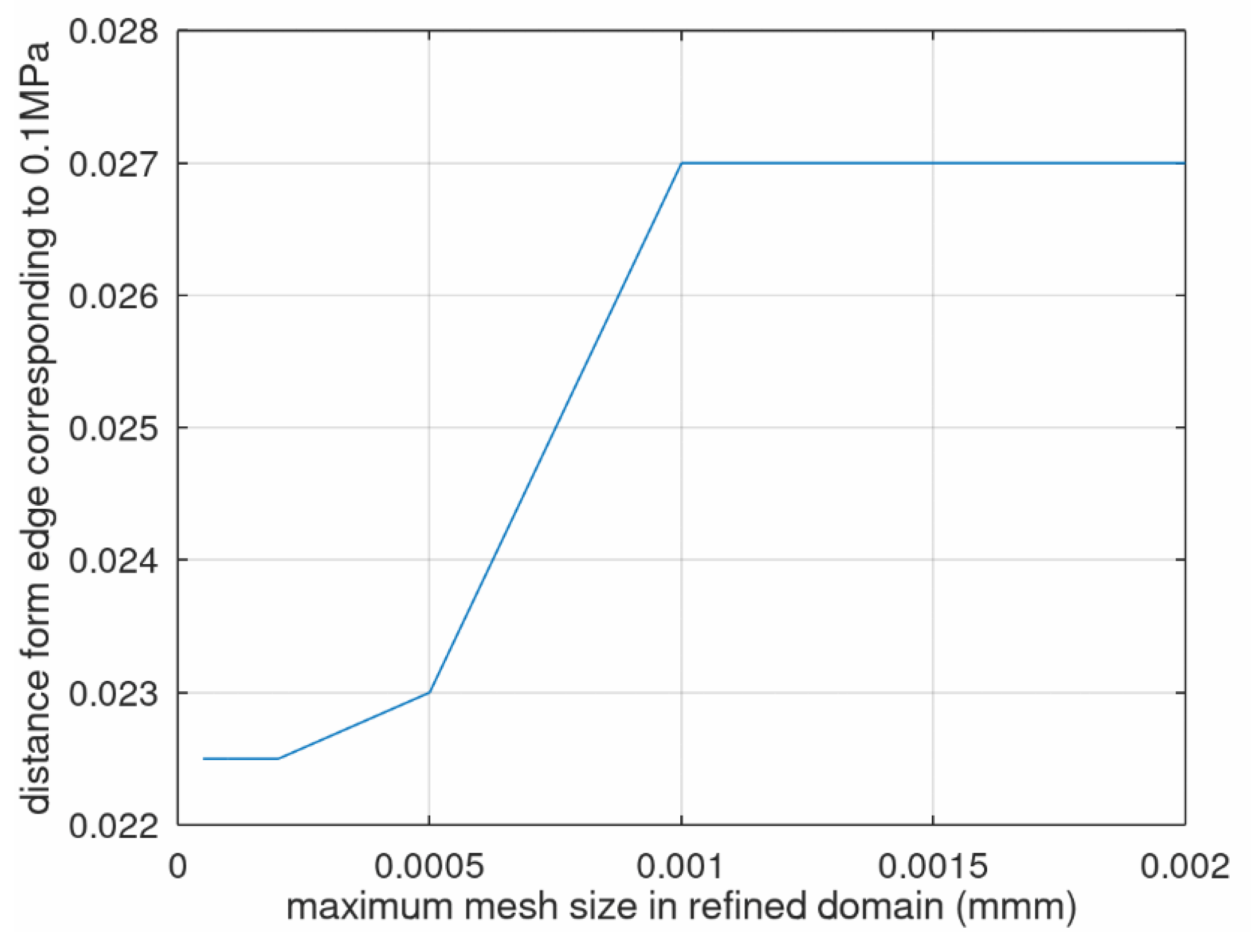
  • Silicone compounds are nearly incompressible; therefore, high local stress builds up near the interface between the substrate and the coating and particularly close to composite edges, demanding a high grid density to obtain a mesh-independent solution. This point is discussed later in the paper.
PCB architectures vary significantly from case to case; therefore, it makes sense to compare performances of conformal coating, starting with simpler geometry, i.e., an assembly substrate/coating. To identify which coating properties to focus on in the development of a soft silicone conformal coating, it is convenient to have analytical solutions obtained, making simplification assumptions valid for those coatings. Analysis of the function solution of solid mechanics equations provides intuition on the most important parameter impacting coating durability and how those parameters vary in improving coating performances.
The calculation of the tensile stress developing in a bi-layer thin sheet has been studied since the 1970s, and simplified formulas have been proposed using plane stress assumption [22].
Considering the generalized Hooke’s law modified to include a strain contribution associated with thermal dilatation and assuming that all stress components along sheet thickness are null (referred to as z direction in Figure 5), i.e., Δ σ z =   Δ   τ y z =   Δ   τ x z = 0 (the plane stress assumption), the relation linking the tensile stress and the tensile strain in a thin sheet is given by:
Δ   ε x = Δ σ x E   ( 1 υ ) + α   Δ   T   and   Δ   ε x = Δ   ε y
With Δ   ε x ,   Δ   ε y the elongation along the x and y direction associated with thermal dilation, Δ σ x , the thermal stress associated with elongation Δ   ε x , υ the Poisson ratio, and α the thermal dilation coefficient.
The next step consists of coupling Equation (2) built for both the substrate and the coating to create a bi-layer material. A condition to guarantee model consistency is to impose that the deformation in both the substrate and the coating are equal at the junction between the two layers, i.e., [ Δ   ε x ] a   = [ Δ   ε x ] s   where subscripts a and s correspond to coating and substrate, respectively. To eliminate the stress in the substrate from Equation (2) and have the stress in the coating be the sole unknown, we know that at equilibrium, the sum of forces is null:
h a   [ Δ σ x ] a + h s   [ Δ σ x ] s = 0
with h a and h s , the thicknesses of the coating and the substrate.
Using (3), the tensile stress induced in the coating by the CTE mismatch between both layers (the substrate and the coating) is calculated:
[ Δ σ x ] a = E a   ( α s α a ) Δ   T ( 1 υ a ) + h a h s   E a E s ( 1 υ s )
We observe that Equation (4) includes thermal and mechanical components via the thermal dilatation coefficient α and Young’s modulus and Poisson’s ratio of the coating and the substrate.
Silicone coatings have a Young’s modulus lower by multiple orders of magnitude than the PCB Young’s modulus, and coating thickness is significantly less than substrate thickness. Therefore, it can be written in good approximation:
[ Δ σ x ] a = E a   ( α s α a ) Δ   T ( 1 υ a )
With those simplification assumptions, we observe that tensile stress is a linear function of both Young’s modulus of the coating and the CTE mismatch. In addition, we notice that lateral tensile stress no longer depends on the thickness of the coating and is not a function of the lateral position with respect to plate edges. Those well-known Formulas (4) and (5) [17,23] are valid for minor deflection of the bi-layer sheet, an assumption valid in present conformal coating application because of the large difference in substrate and coating thickness and the low elastic modulus of silicone materials.
Equation (5) provides a reasonable estimate of the lateral tension stress build-up associated with the difference in CTE between the two bi-layer materials. Lateral tension stress has no spatial dependence, assuming the stress is constant along the interface plane. Therefore, it cannot predict coating delamination often observed at the edge of the plate. Restricting material evaluation to Equation (5) does not consider the large shear stress that can develop close to the edges of the bi-material sheet. When moving away from the bi-layer plate edge, shear stress decreases to become negligible, and tension stress becomes dominant. Including localized spatial shear stress in the coating evaluation is important because high shear stress near the edge can initiate delamination. Freund and Hu have studied [24] the shear stress distribution considering thin film assumptions, the film being thin enough to be modeled as a membrane. Authors propose an integrodifferential equation predicting shear stress spatial distribution along the lateral plate’s dimension (along x or y in Figure 5) in the function of an imposed strain (that can be associated with a CTE mismatch). They derived two approximated analytical solutions of the stress distribution equation, one solution valid close to the edge of the bi-layer plate and one valid far from the edge. Defining ξ = E s   ( 1 ν a 2 ) E a ( 1 ν s 2 )   x h a , a dimensionless variable of the lateral position x (position x is multiplied by a factor function of both coating and substrate mechanical properties and coating thickness), the approximated shear stress distribution near the edge (valid for small ξ values, comprised between 0 and 2) takes the form:
τ x   E s   ( 1 ν a 2 ) Δ T   ( α s α a ) ( 1 ν a ) ( 1 ν s 2 )   [ ( 2 π   ξ ) 1 2 0.21938   ξ 1 2 + 0.12698   ξ 1 2   l n   ( ξ ) ]
When moving apart from the edge, the shear stress component decreases rapidly, and for ξ values > 5, an approximated value of shear stress spatial evolution is given by:
τ x   E s   ( 1 ν a 2 ) Δ T   ( α s α a ) ( 1 ν a ) ( 1 ν s 2 )   [ 2 π ξ 2 4   4 π 2 ξ 3   ( 1.2319 2 ln ( ξ ) ) ]
Analysis of the dimensionless variable ξ , ξ takes large values very near the edge x h a when a large difference exists between Young’s modulus of the substrate and Young’s modulus of the coating, which is the case for the application studied in this paper. The evolution of ξ in the function of x h a , the normalized distance from the edge is shown in Figure 6, using the mechanical properties of both the PCB substrate and conformal coating A measured at 125 °C (Table 2). It is observed that we are outside the domain of validity of Equation (6) for x h a > 2.0 × 10⁻⁴ (a distance of 2.0 × 10⁻⁵ for a coating of 0.1 mm thickness), meaning that the high shear predicted by Equation (6) is very localized and decreases very rapidly when moving apart from the edge of the bi-layer sheet.
Figure 7 shows the evolution of the shear stress in the function of distance from the edge, calculated for ξ values > 5 that corresponds to the domain of validity of the far edge approximated solution (7). A sharp stress decrease is observed, stress dropping to a value of 0.03 MPa at a distance equal to the hundredth of film thickness.
The large stress predicted by simplified Formula (7) results from the nearly full incompressible nature of the conformal coating. The plane of adhesion between the PCB and the coating restricts the free deformation of the coating required to conserve the volume, creating a local high shear stress. For comparison, solid mechanics equations are solved for a 2D geometry using a COMSOL FEA model (Figure 8). A multiphysics model (solid mechanics and thermal transfer) is built to have the stress induced in the coating coming from the CTE mismatch between the conformal coating and the PCB. The stress is assumed null at 20 °C, and the steady state stress that builds up when increasing temperature up to 125 °C is calculated. All the boundaries of the coating and the PCB in contact with the external environment are set at 125 °C, which corresponds to the equilibrium temperature in an oven at this temperature. Because simplified formulae are derived assuming a linear elastic material, a linear material model approximation was used for the FEA model, with the material properties given in Table 2.
The conformal coating thickness is taken equal to 0.1 mm; therefore, a distance equal to 0.0001 mm from the edge corresponds to an x/ha value of 0.001 in Figure 7. A free triangular mesh discretization is used with a cubic Lagrange shape function to obtain a more accurate description of the deformation near the edge for a fixed number of cells. An example of stress evolution when moving away from the edge is shown in Figure 9. A sharp stress decrease is observed when moving away from the edge to converge to a constant spatial stress value. This observation confirms the prediction of the simplified model.
The stability of the FEA solution was studied by looking at two parameters: (1) the evolution of the Von Mises stress value at 0.001 mm from the edge when decreasing the maximum size of cells in the zone close to the edge (Figure 10); (2) the value of the distance from the edge corresponding to a stress value equal to 0.1 MPa (Figure 11). For both criteria, Figure 10 and Figure 11 shows that a stable solution exists for a mesh scheme characterized by a cell’s maximum dimension lower or equal to 0.0005 mm in the region near the edge. The stress value calculated by FEA is 1.6 MPa compared to 6 MPa obtained from Figure 9.
A Von Mises stress equal to 1.6 MPa calculated 0.0001 mm apart from the edge is not the maximum stress experienced by the coating. Figure 9 shows that Von Mises stress further increases when moving closer to the composite edge. The stress calculated at a shorter distance of 5 × 10⁻⁵ mm from the edge with a 1 × 10⁻⁵ mm mesh cell size gives a stress value of 16 MPa.
The steep stress nonlinear increase close to the edge makes the discretization process complex, requiring a very accurate meshing scheme. Full incompressibility, i.e., a Poisson ratio of 0.5, leads to a singularity close to the interface between the coating and the PCB substrate. The Poisson ratio has been measured in a very accurate way on silicone compounds [25], and decreasing the Poisson value to stabilize the solution is not an acceptable method. For this reason, when carrying out FEA models, having analytical reference formulas are a big help in validating the order of magnitude of the FEA solution and also in guiding the mesh range to explore obtaining a stable solution.

3.3. Testing Stress Predictions of Simplified Model Compared to the Stress Distribution Calculated Using FEA Code for the Case of a Bi-Layer Thin Plate

Lateral tension stress in the films calculated using equation 5 is compared to stress values calculated far from bi-layer strip edges using a 2D FEA COMSOL model of a bi-layer sheet. This stress corresponds to the constant stress value along composite length observed far from the edges where the shear stress contribution becomes negligible (Figure 9). The constant stress value at the center of the strip corresponds to the lateral tension stress calculated using Equation (5), lateral tension stress being the dominant contribution to the Von Mises stress far from the edges. The parameters used to build the material’s model are the ones used in paragraph 3.3 and given in Table 2. Not studying the sharp stress profile close to the edges allows the use of a looser mesh in the FEA model build-up without impacting the calculated stress value.
An example of the FEA result is shown in Figure 12 for coating A exposed to −40 °C. Similar stress spatial profiles are observed for coatings A and B at low and high temperatures that will not be shown here. Von Mises stress values in the center of the strip (equal to lateral tension stress) are compared to the stress calculated using equation 5 for all explored conditions (coating type and temperature exposure). Results summarized in Table 3 show agreement between the FEA and the simplified approach.

3.4. Comparing Stresses Calculated Either by Simplified Model or FEA to the Local Stress Threshold Leading to Silicone Failure

Lateral tensile stress and local shear stress near strip edges induced by temperature changes have been calculated using simplified and 2D FEA models of the bi-layer strip. The next step is to evaluate if those stresses are large enough to initiate a local failure in the coating. Therefore, the local stress threshold that creates coating failure under uniaxial tension is measured for both coating A and B using dog bone test pieces, with the engineering stress value at the break being recorded. The choice of a dog bone (or uniaxial test piece) is made because test piece geometry is designed to allow free reduction of the cross-section when pulling (to conserve the volume of silicone, a nearly incompressible material). Therefore, the local stress value is constant over all test piece volume and directed towards the pulling direction. In PCB conformal coating application, coating thickness is generally ~0.1 mm. It is very difficult to prepare thick samples with those materials; therefore, dog bones 0.1 mm thick were prepared for material characterization. Three specimens are used for the traction test experiment to determine the parameters of both linear and Neo-Hookean models. Figure 13 shows the strain-strain curve measured on coating B at 125 °C.
In Figure 13, the line of magenta color is the Neo-Hookean model used to fit the nonlinear behavior of the material measured at large elongation. This Noe-Hookean hyperelastic behavior is plotted using the Lame parameter identified from bog bones made of coating B and tested at 125 °C. The blue straight-line curve corresponds to the linear model, the two models (the linear and Neo-Hookean) superposing for small elongations. Three dog bones were used to understand reproducibility. The replication of the stress-strain testing shows curves superposing, allowing an accurate estimate of both linear and nonlinear models. Larger variations are observed for both the stress and the strain value at the break, those two quantities being more sensitive to defects created during sample preparation. Table 4 below shows the average tensile strength and elongation at break for different conformal coatings and their related standard deviations.
Note that conformal coating A has a much higher (4.0 times) tensile strength and slightly lower (36.0%) elongation at break than conformal coating B. In a uniaxial traction experiment, the engineering tensile stress provided by the testing equipment is calculated dividing the force by the x-section of the test piece before the traction force is applied. However, when pulling progresses, the x-section reduces to conserve volume. For this reason, to convert the tensile stress (engineering stress) into real stress, the x-section change when elongating the material is calculated:
S S = ( 1 + ε )   2 υ
With S, the cross-section at rest, and S′, the cross-section at the elongation ε ; υ is the Poisson ratio. The real stress associated with failure is calculated from measured engineering stress at break:
σ l o c a l = σ t e n s i o m e t e r S S
The stress at rupture measured on dog bones is compared to the lateral tension stress away from the edges calculated using FEA code and Equation (5). Shear stress values very close to the edge calculated using either equation 7 or FEA models in paragraph 3.2 are much larger stress (16 MPa) than the stress corresponding to coating failure. Therefore, delamination should be observed when increasing temperature from the temperature at which the conformal coating was applied (25 °C) to the temperature of 125 °C at which shear stress values are calculated. However, the area of shear stress value being very localized near the edge and followed by a sharp decrease, we may assume that localized delamination resulting from large shear stress allows stress relaxation, preventing crack propagation over long distances from the edge. We did not observe any delamination near the edges of the conformal coatings A or B exposed to the temperature cycle. Therefore, we concluded that shear stress near the strip edge is not an appropriate criterion for silicone conformal coating evaluation and selection. Therefore, we focus below on the sole lateral tensile stress component calculated using either Equation (5) or FEA to select the conformal coating best suitable for both applications. Conformal coating tensile performance compared with calculated and FEA modeling of lateral tensile stress is summarized in Table 5. For conformal coating A, the lateral tensile stress calculated at −40 °C is nearly equal to 51% of the stress measured at rupture, showing a rather low safety margin compared to coating failure. On the contrary, the safety margin concerning rupture is large at 125 °C (calculated stress is less than 1% of the stress leading to failure). This result is explained by Young’s very large modulus value measured at low temperatures. For conformal coating B, the conclusion is different because Young’s modulus value is more stable with temperature. Therefore, stress values show less difference between cold and hot temperatures, having larger stress observed at 125 °C. We also observe a lower tensile strength value of coating B recorded on dog bones, having the stress calculated at 125 °C corresponding to ~5% of the stress at break. For a bi-layer sheet, we identified two conditions potentially critical for the two coatings being tested, the low-temperature part of the temperature cycle (−40 °C) for conformal coating A and the high-temperature part of the cycle for conformal coating B (corresponding to 125 °C).

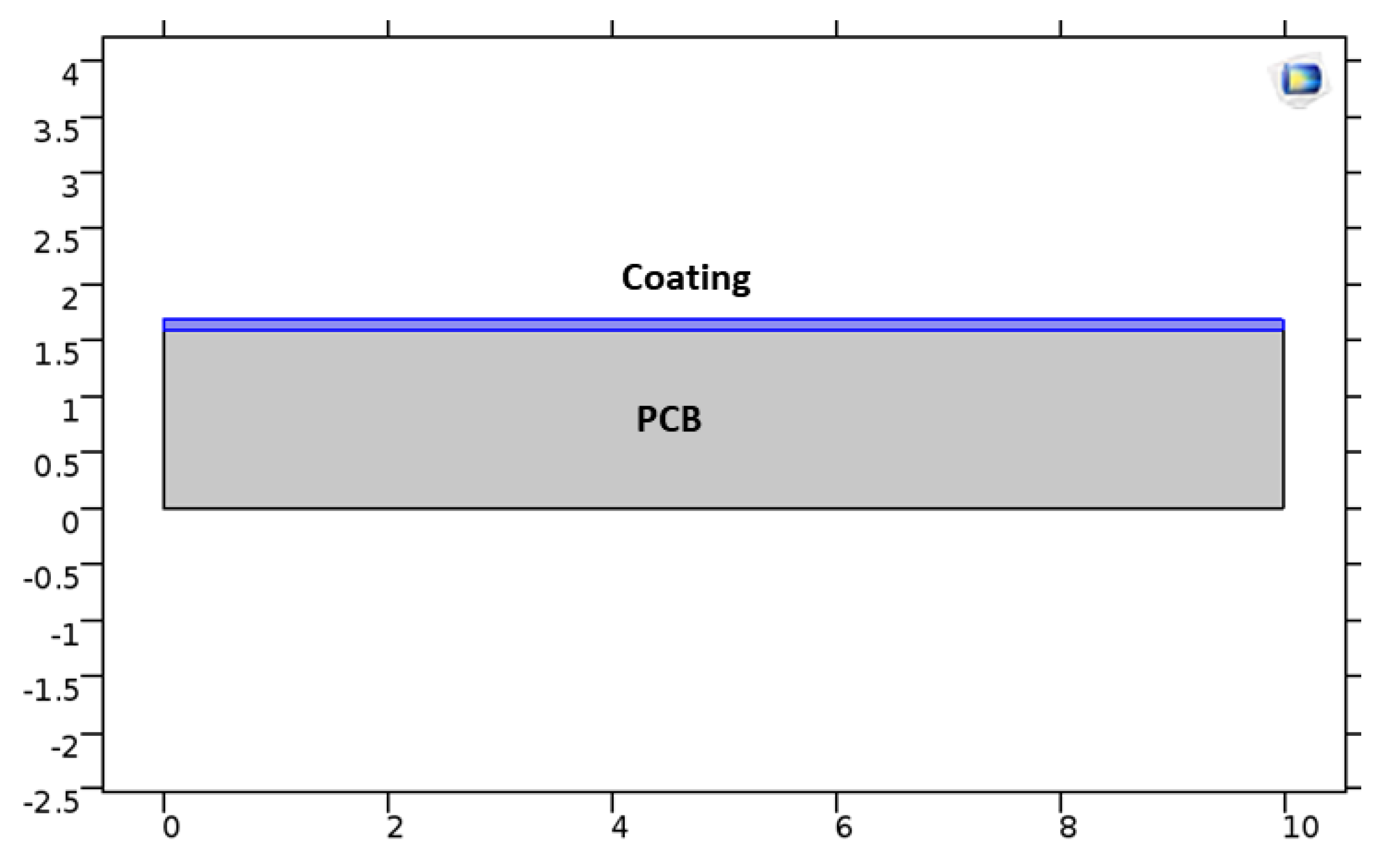
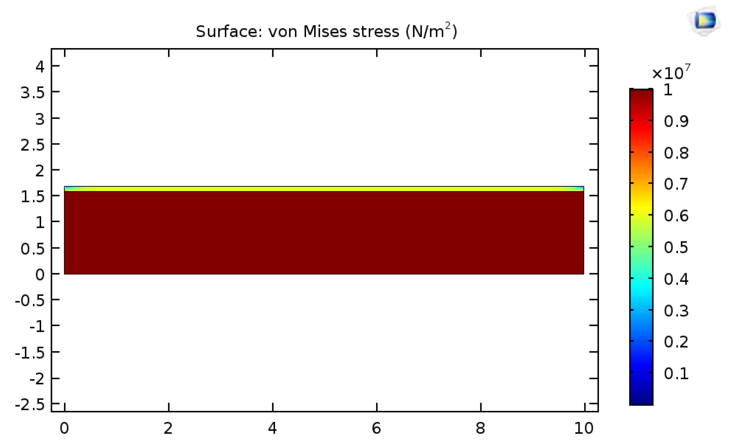
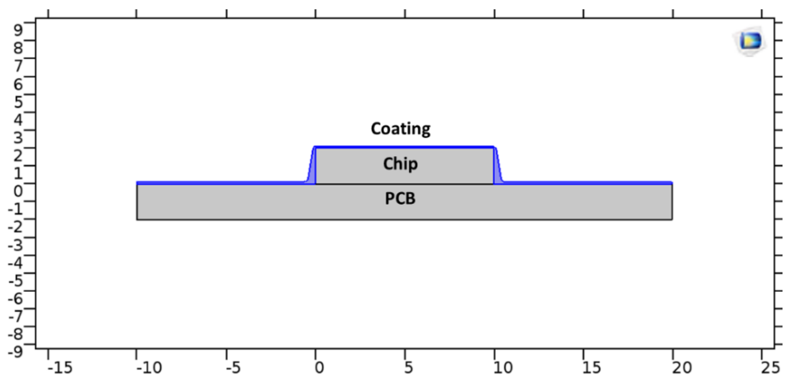
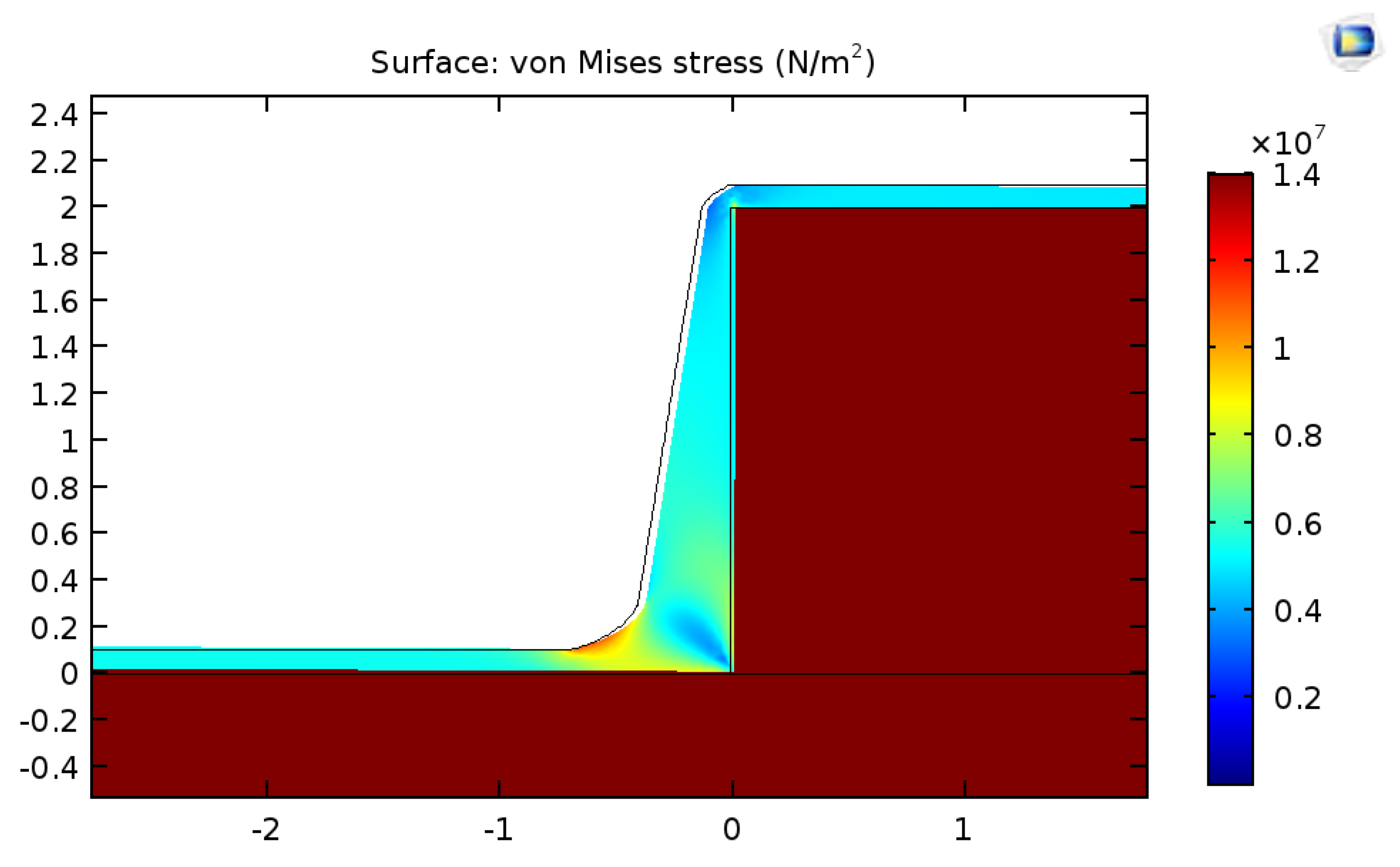
3.5. D FEA Modeling of the Stress Distribution for the Case with Chip Attached to the PCB

When restricting the study to lateral tension stress component criteria, the simple bi-layer geometry studied before is less severe than that observed in conformal coating applications. Chips attached to the PCB and covered by the coating likely create local high-stress values. For this reason, a more complex geometry (Figure 14) is studied using a 2D FEA model.
Because of the presence of the chip, new zones of high stress are expected at the junction between the PCB and the chip or the upper left and right corners of the chip. Therefore, a new mesh study is required to test the stability of the solution in the vicinity of the chip. Rounded corners are used for the coating covering the corners of the chips to consider either coating accumulation at the lower edges, close to the PCB, and thinner coating at the upper left and right corners of the chip. The control physics default mesh of COMSOL was used for meshing, which is based on a triangular element with a quadratic Lagrange shape function. The spatial stress distribution building in coating A when exposed to a temperature of 125 °C was calculated by varying the mesh density. We looked at the stress close to the lower edge of the chip because it is where larger stress builds up because of the presence of two orthogonal adhesion interfaces. The evolution of stress in the function of the number of triangular elements is summarized in Table 6, showing the rather stable mesh insensitive solution is obtained for 1748 elements.
To provide a more accurate local stress estimate, the linear elastic assumption is removed, selecting a Neo-Hookean nonlinear model that provides a better fit of the experimental stress-strain curve for larger strain values. The Neo-Hookean model shows that its nonlinear behavior is fully defined by Young’s modulus calculated in the linear part of the measured stress-strain curve, corresponding to low strain values. The Lame parameters inputs to COMSOL are calculated using Young’s modulus and Poisson’s ratio. Material parameters are summarized in Table 7. Table 8 shows chip and PCB material properties used in FEA simulation. The chips are usually packaged by an epoxy molding compound; therefore, epoxy resin properties were selected for FEA simulation. While a Neo Hookean hyperelastic model was identified from experimental results, a linear material was used for both PCB and epoxy components.
FEA simulation of stress distribution in conformal coating A on PCB substrates at the temperature of −40 °C and +125 °C are shown in Figure 15 and Figure 16. The local stress is expressed using the Von Mises stress, which is related to the energy of deformation of the material. As an alternative, another option would be to plot the first principal stress. Still, it is anticipated that due to complex geometry, there are spatial regions where the second and third principal stresses are not negligible compared to the first component. In the case of only considering the first principal component, we would neglect non-negligible stress components.
High local stress is observed near the junction between the chip and the PCB board, leading to a stress value twice greater than the constant tensile tress spatial distribution away from the chip. Similar stress distributions are observed for coating B, not shown here. The maximum stress calculated for both coatings and different conditions is summarized in Table 9.
For coating A, stress of 10.65 MPa is calculated at −40 °C and a value of 0.16 MPa at 125 °C. The max. local stress calculated at −40 °C reaches ~94% of the local stress measured at rupture, while the safety margin concerning rupture is large at 125 °C (1.4%). In terms of coating suitability for conformal coating application, we have similar conclusions to those obtained using simpler bi-layer geometry: high temperature leads to a low local stress value compared to the value at rupture, while potential failure is possible at low temperature. The presence of the chip makes the local stress value almost equal to the threshold of stress rupture, with a high potential risk of crack initiation with time. For conformal coating B, the max. local stress value near the chip is 0.16 MPa at −40 °C and 0.44 MPa at 125 °C, respectively. As predicted by the simplified approach, the issue now is at high temperatures, for which we have higher stress. Because the max. local stress value remains below 13% of the stress leading to rupture, the risk of potential crack stays low.

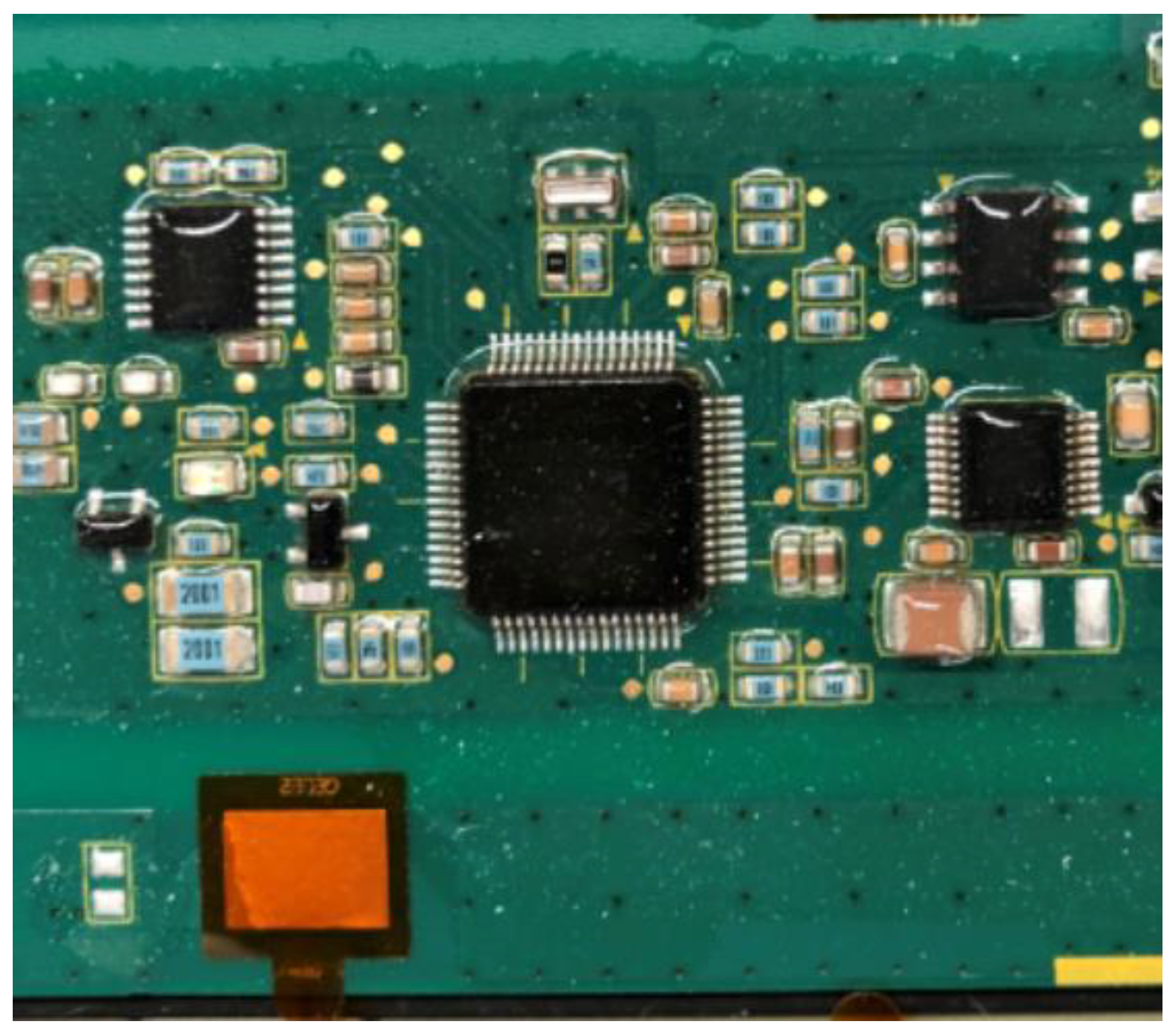
3.6. Experimental Observation: Reliability Test

PCBs coated with conformal coating A and B were prepared for a reliability performance study. Aging conditions, including thermal shock (TS) and thermal cycling (TC), are described in the 2.4 paragraph. Reliability results are summarized in Table 10. We observed that conformal coating A passed 517 thermal shocks without cracks, while cracks appeared after 350 cycles of thermal cycling (Figure 17). Conformal coating B pass 3 rounds of 517 thermal shocks followed by 517 cycles of thermal cycling (Figure 18). These results agree with the conclusions of the proposed evaluation method that conformal coating A shows lower performance in cases of extreme external stress exposure compared to conformal coating B. Coating B is, therefore, more appropriate and is recommended for applications requiring stability under extended thermal shock and thermal cycling PCB operating conditions. This result also aligns with the previous discussion about the importance of both CTE and mechanical properties’ impact on material failure and criteria for coating selection. From the above study, it is concluded that conformal coating A is more suitable for applications requiring higher anti-scratch performance and less thermal shock/ cycling needs. Conformal coating B is more suitable for harsh thermal shock/ cycling resistance requirement applications, highlighting the benefit of using a highly deformable material under extreme operating conditions.

4. Conclusions

Silicone conformal coatings have low elastic modulus (elastic modulus multiple orders of magnitude lower than substrate modulus) compared to alternative chemistries used in conformal coating applications for the electronic industry. Soft coatings make established test methods (for example, the bi-material strip bending) no more appropriate for coating evaluation but, in counterpart, offer opportunities to establish new test methods building on this specificity. To achieve this goal, a study was initiated combining simplified solutions of solid mechanics equations, 2D FEA models, and experimental observations.
The bi-material strip bending, a well-known and easy-to-carry-out technique for evaluating the ability of bi-layer composites to sustain imposed deformations, is not appropriate for selecting soft conformal coatings used for PCB protection. The method imposes a bending of the composite that does not take place during exposure to large temperature variations, the soft coating following the deformation imposed by the differential thermal dilation between components. For this reason, different routes were explored and tested to identify a consistent method to evaluate the performances of soft coating submitted to thermal stress. Soft coatings of Young’s modulus at least 3 orders of magnitudes lower than other components of the PCB substrate:
  • Allows simplified analytical solution of solid mechanics equations to calculate both the high shear stress dominant close to the edges and the lateral tension stress dominant far from the edges where shear stress becomes ~0;
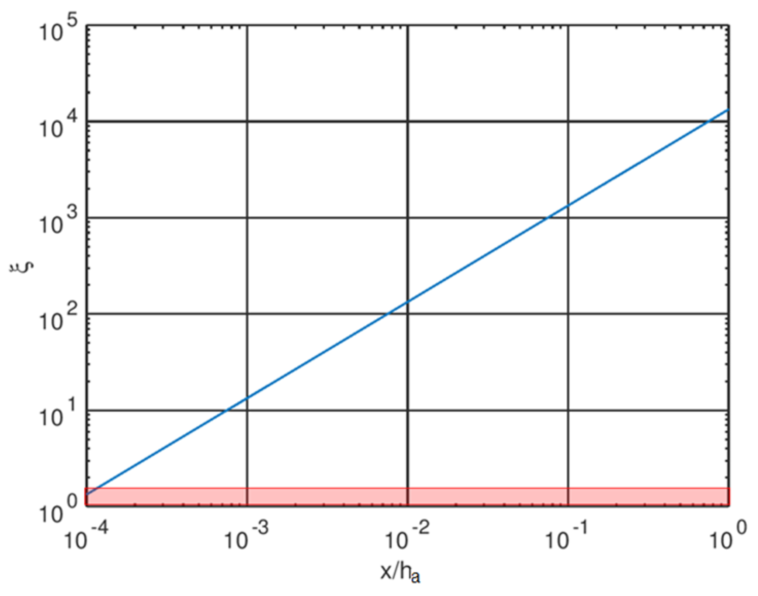
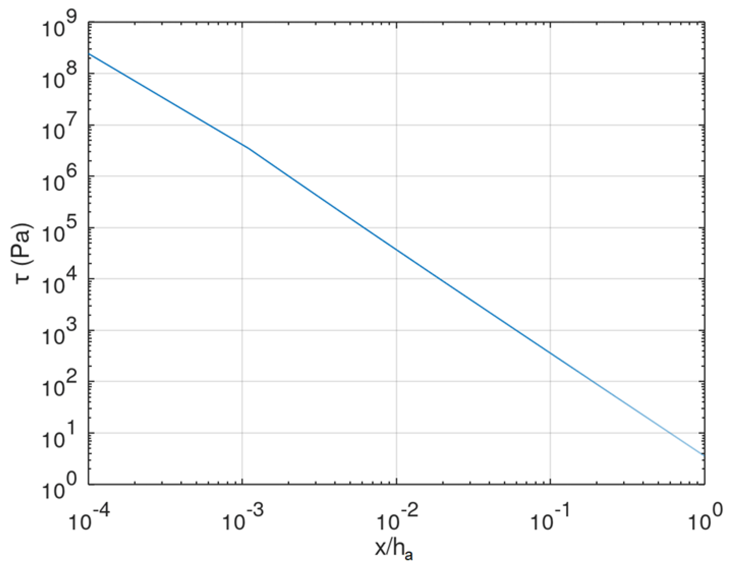
  • Creates a very localized high shear stress close to the edges, confirmed by the analysis of the analytical shear stress solution that demonstrates that high shear stress decreases very abruptly over a very short distance when the elastic modulus of the coating is much smaller than the elastic modulus of the substrate;
  • Makes FEA models of shear stress near the edge complex, requiring mesh spatial density and cell dimensions differing by order of magnitude, the extent of the nonlinear shear stress decrease being ~10−3 mm. Therefore, a simplified solution offers benefits for checking the outcome of FEA models and guiding the build-up of the meshing scheme;
  • The modeling and stress calculation are combined with an experimental part;
  • Measurement of the stress threshold that leads to rupture carried out using dog bone test pieces;
  • PCB specimens with electronic components are submitted to temperature cycles with extreme low and high temperatures equal to the temperatures used in both simplified and FEA models. Optical microscope observation of potential cracks appearance is carried out, and their correspondence with the regions of modeled high stress is studied.
The high shear stress that builds up close to the edges predicts the failure of both coatings A and B when exposed to low and high-temperature cycles. However, no defects or delamination are observed at composite edges after thermal cycling. The reason is likely the very narrow extent of the high shear region and the steep drop from 16 MPa to 0.3 MPa over a 10−3 mm distance, which leads to stress relaxation. On the contrary, lateral tension stress calculated either by the simplified model or FEA succeeds in explaining the cracks observed on a commercial PCB board exposed to thermal cycles. This positions the lateral tension stress as the most appropriate criterion for rapid soft coating evaluation, the accuracy of analytical solutions allowing the evaluation of how each parameter impacts stress-associated temperature variations.

Author Contributions

Conceptualization, L.Z. and P.D.; lab test, L.Z.; FEA simulation, L.Z. and P.D.; writing-original draft preparation, L.Z.; writing-review and editing, P.D. All authors have read and agreed to the published version of the manuscript.

Funding

This research received no external funding.

Institutional Review Board Statement

Not applicable.

Informed Consent Statement

Not applicable.

Data Availability Statement

Not applicable.

Acknowledgments

The authors would like to acknowledge François De Buyl, Nick Shephard, and Junying Liu from Dow Chemical Company for reviewing the paper and for their relevant suggestions.

Conflicts of Interest

The authors declare no conflict of interest.

References

  1. Weide-Zaage, K. Simulation of packaging under harsh environment conditions (temperature, pressure, corrosion and radiation). Microelectron. Reliab. 2017, 76–77, 6–12. [Google Scholar] [CrossRef]
  2. Abbas, A.-A.F.; Pandiarajan, G.; Iyer, S.; Greene, C.; Santos, D.; Srihari, K. Impact of conformal coating material on the long-term reliability of ball grid array solder joints. IEEE Trans. Compon. Packag. Manuf. Technol. 2020, 10, 1861–1867. [Google Scholar] [CrossRef]
  3. Pippola, J.; Marttila, T.; Frisk, L. Protective coatings of electronics under harsh thermal shock. Microelectron. Reliab. 2014, 54, 2048–2052. [Google Scholar] [CrossRef]
  4. Sivakumar, P.; Du, S.M.; Selter, M.; Daye, J.; Cho, J. Improved adhesion of polyurethane-based nanocomposite coatings to tin surface through silane coupling agents. Int. J. Adhes. Adhes. 2021, 110, 102948. [Google Scholar] [CrossRef]
  5. Han, S.; Osterman, M.; Meschter, S.; Pecht, M. Evaluation of Effectiveness of Conformal Coatings as Tin Whisker Mitigation. J. Electron. Mater. 2012, 41, 2508–2518. [Google Scholar] [CrossRef]
  6. Sivakumar, P.; Du, S.M.; Selter, M.; Ballard, I.; Daye, J.; Cho, J. Long-term thermal aging of parylene conformal coating under high humidity and its effects on tin whisker mitigation. Polym. Degrad. Stab. 2021, 191, 109667. [Google Scholar] [CrossRef]
  7. Suppa, M. Conformal Coatings for Electronics Applications; Lackwerke Peters: Kempen, Germany, 2012. [Google Scholar]
  8. Keeping, J. Conformal Coatings. In Lead-Free Soldering Process Development and Reliability; Bath, J., Ed.; John Wiley & Sons: Hoboken, NJ, USA, 2020. [Google Scholar]
  9. Pippola, J.; Marttila, T.; Frisk, L. Effect of Protective Casting Materials on Product Level Reliability under Accelerated Test Conditions. In Proceedings of the 2013 European Microelectronics Packaging Conference (EMPC), Grenoble, France, 9–12 September 2013; pp. 1–6. [Google Scholar]
  10. Lowndes, R.; Cotton, I.; Emersic, C.; Rowland, S.; Freer, R. Thermal Stresses of Conformal Coatings on Printed Circuit Boards. In Proceedings of the 2015 IEEE Electrical Insulation Conference (EIC), Seattle, WA, USA, 7–10 June 2015; pp. 106–109. [Google Scholar]
  11. Serebreni, M.; Wilcoxon, R.; Hillman, D.; Blattau, N.; Hillman, C. The Effect of Improper Conformal Coating on SnPb and Pb-Free BGA Solder Joints During Thermal Cycling: Experiments and Modeling. In Proceedings of the 2017 33rd Thermal Measurement, Modeling & Management Symposium (SEMI-THERM), San Jose, CA, USA, 13–17 March 2017; pp. 40–47. [Google Scholar]
  12. Emersic, C.; Lowndes, R.; Cotton, I.; Rowland, S.; Freer, R. The Effects of Pressure and Temperature on Partial Discharge Degradation of Silicone Conformal Coatings. IEEE Trans. Dielectr. Electr. Insul. 2017, 24, 2986–2994. [Google Scholar] [CrossRef] [Green Version]
  13. Reedy, E.D. Tensile cracking of a brittle conformal coating on a rough substrate. Int. J. Fract. 2016, 199, 245–250. [Google Scholar] [CrossRef]
  14. Francis, L.F.; Mccormick, A.V.; Vaessen, D.M.; Payne, J.A. Development and measurement of stress in polymer coatings. J. Mater. Sci. 2001, 37, 4717–4731. [Google Scholar] [CrossRef]
  15. Wang, X.S.; Tang, H.P.; Li, X.D.; Hua, X. Investigations on the Mechanical Properties of Conducting Polymer Coating-Substrate Structures and Their Influencing Factors. Int. J. Mol. Sci. 2009, 10, 5257–5284. [Google Scholar] [CrossRef] [PubMed]
  16. Biernath, R.W.; Soane, D.S. Characterization of Stresses in Polymer Films for Microelectronics Applications. In Polymeric Materials for Electronics Packaging and Interconnection; Lupinski, J.H., Moore, R.S., Eds.; American Chemistry Society: Washington, DC, USA, 1989. [Google Scholar]
  17. Sham, M.-L.; Kim, J.-K. Evolution of residual stresses in modified epoxy resins for electronic packaging applications. Compos. Part A 2004, 35, 537–546. [Google Scholar] [CrossRef]
  18. Lee, S.; Lee, C.W.; Kim, C.S. FEA Study on the Stress Distributions in the Polymer Coatings of Cardiovascular Drug-Eluting Stent Medical Devices. Ann. Biomed. Eng. 2014, 42, 1952–1965. [Google Scholar] [CrossRef] [PubMed]
  19. Liu, Y.; Chen, Y.-C.; Hutchens, S.; Lawrence, J.; Emrick, T.; Crosby, A.J. Directly Measuring the Complete Stress–Strain Response of Ultrathin Polymer Films. Macromolecules 2015, 48, 6534–6540. [Google Scholar] [CrossRef]
  20. Nazir, M.H.; Khan, Z.A. A review of theoretical analysis techniques for cracking and corrosive degradation of film-substrate systems. Eng. Fail. Anal. 2017, 72, 80–113. [Google Scholar] [CrossRef]
  21. Naebe, M.; Abolhasani, M.M.; Khayyam, H.; Fox, A.B. Crack Damage in Polymers and Composites: A Review. Polym. Rev. 2016, 56, 31–69. [Google Scholar] [CrossRef]
  22. Timoshenko, S.P.; Goodier, J.N. Theory of Elasticity; McGraw-Hill: New York, NY, USA, 1970. [Google Scholar]
  23. Astapov, A.N.; Nushtaev, D.V.; Rabinskiy, L.N. Calculation of Thermal Stresses in a Substrate−Coating System. Compos. Mech. Comput. Appl. Int. J. 2017, 8, 267–286. [Google Scholar] [CrossRef]
  24. Freund, L.B.; Hu, Y. Shear Stress at a Film-Substrate Interface Due to Mismatch Strains; Brown University Report; Brown University: Providence, RI, USA, 1988. [Google Scholar]
  25. Wolf, A.; Descamps, P. Determination of Poisson’s Ratio of Silicone Sealants from Ultrasonic and Tensile Measurements. In Performance of Exterior Building Walls; Johnson, P., Ed.; ASTM International: West Conshohocken, PA, USA, 2003; pp. 132–142. [Google Scholar]
Figure 1. Prepare silicone conformal coating A and B films with an auto film applicator.
Applsci 12 11268 g001
Figure 2. Silicone conformal coating A and B dog bone for tensile test.
Applsci 12 11268 g002
Figure 3. (a) Thermal shock and (b) thermal cycling aging conditions.
Applsci 12 11268 g003
Figure 4. Schematic view of BMSB modeling.
Applsci 12 11268 g004
Figure 5. Conformal coating on PCB substrate schematic view picture.
Applsci 12 11268 g005
Figure 6. Evolution of ξ in the function of the distance from the plate edge being normalized by film thickness. The red rectangle represents the domain of validity of the close-edge approximated solution.
Applsci 12 11268 g006
Figure 7. Shear stress calculated using equation 7 of the far edge approximated solution in function of the distance from the plate edge being normalized by film thickness.
Applsci 12 11268 g007
Figure 8. Geometry of 2D FEA modeling of a bi-layer sheet; x, y units are in mm.
Applsci 12 11268 g008
Figure 9. Evolution of the Von Mises Stress when moving away from the edge of the strip.
Applsci 12 11268 g009
Figure 10. Von Mises stress evolution with the change of the maximum cell size in the domain close to the edge.
Applsci 12 11268 g010
Figure 11. Evolution of the distance from the edge that corresponds to a Von Mises stress equal to 0.1 MPa when changing the maximum cell size in the domain close to the edge.
Applsci 12 11268 g011
Figure 12. FEA modeling of conformal coating A stress distribution at −40 °C; x, y units are in mm.
Applsci 12 11268 g012
Figure 13. Conformal coating B tensile profile.
Applsci 12 11268 g013
Figure 14. Geometry of 2D FEA modeling of chip attached to PCB; x, y units are in mm.
Applsci 12 11268 g014
Figure 15. FEA modeling of conformal coating A stress distribution at −40 °C; x, y units are in mm.
Applsci 12 11268 g015
Figure 16. FEA modeling of conformal coating A stress distribution at 125 °C; x, y units are in mm.
Applsci 12 11268 g016
Figure 17. PCB coated with Conformal Coating A, showing cracks after 517 cycles of thermal shocks and 350 cycles of thermal exposure, as described in the text.
Applsci 12 11268 g017
Figure 18. PCB coated with Conformal Coating B, passing 3 rounds of 517 thermal shocks followed by 517 cycles of thermal cycling without cracking, as described in the text.
Applsci 12 11268 g018
Table 1. Conformal coating material properties.
MaterialUnitConformal Coating AConformal Coating B
ViscositymPa·s1050350
Tack-free time (25 °C)Mins68
Densityg/cm31.120.98
HardnessShore A8534
Elastic modulus (25 °C)MPa77.11.50
CTEppm/K300490
Dielectric strengthkV/mm1317
Volume resistivityOhm·cm1.9 × 10145.5 × 1015
Table 2. Material properties input used for both the simplified model and the 2D FEA model.
PerformanceUnitCoating A
(−40 °C)
Coating A
(125 °C)
Coating B
(−40 °C)
Coating B
(125 °C)
PCB
DensityKg/m3112011209809801900
Thermal ConductivityW/(m·K)0.20.20.20.20.3
Heat CapacityJ (Kg·K)15001500150015001369
CTE1/K3.0 × 10−43.0 × 10−44.9 × 10−44.9 × 10−41.8 × 10−5
Young’s Modulus EMPa160.11.281.331.9222000
Poisson’s ratio γNA0.490.490.490.490.15
Table 3. Conformal coating tensile lateral stress calculation.
PropertyUnitCoating ACoating B
Tensile stress in x direction (−40 °C, 2D Equation (5))MPa5.770.08
Tensile stress in x direction (−40 °C, 2D FEA model) MPa5.980.08
Tensile stress in x direction (125 °C, 2D Equation (5))MPa0.070.18
Tensile stress in x direction (125 °C, 2D FEA model) MPa0.070.16
Table 4. Tensile data of conformal coatings.
PropertyUnitCoating A Coating B
Tensile strengthMPa5.541.40
Tensile strength standard deviationMPa0.080.26
Elongation%104.4142.0
Elongation standard deviation%1.38.2
Table 5. Conformal coating tensile performance compared with calculated and FEA modeling of lateral tensile stress.
PropertyUnitCoating ACoating B
Corresponding local stress in the dog bone during tensile testMPa11.333.39
Tensile stress in x direction (−40 °C, 2D Equation (5))MPa5.770.08
Tensile stress in x direction (−40 °C, 2D FEA model) MPa5.980.08
Tensile stress in x direction (125 °C, 2D Equation (5))MPa0.070.18
Tensile stress in x direction (125 °C, 2D FEA model) MPa0.070.16
Table 6. Evolution of the maximum value of Von Mises stress near the chip edge in contact with the PCB.
Number of Triangular ElementsNumber of Cell’s VerticesMaximum Von Mises Stress (MPa)
9145230.15
11966700.19
17489600.21
302416270.21
Table 7. Material Lamé parameters input in 2D FEA modeling.
PerformanceUnitCoating A
(−40 °C)
Coating A
(125 °C)
Coating B
(−40 °C)
Coating B
(125 °C)
Lamé parameters λMPa2642.3821.3821.8731.57
Lamé parameters μMPa53.930.440.450.64
Table 8. Chip and PCB material properties input in 2D FEA modeling.
PerformanceUnitChip PCB
Density Kg/m312001900
Thermal ConductivityW/(m·K)0.20.3
Heat CapacityJ (Kg·K)11001369
CTE1/K5.0 × 10−51.8 × 10⁻⁵
Young’s Modulus EMPa10,00022,000
Poisson’s ratio γNA0.300.15
Table 9. Conformal coating max. local stress by 2D FEA modeling of chip attached to PCB.
PropertyUnitCoating A Coating B
Max. local stress (−40 °C, 2D FEA model) MPa10.650.15
Max. local stress (125 °C, 2D FEA model)MPa0.160.44
Table 10. Conformal coating reliability test.
Conformal CoatingCoating Crack Observation
ANo Crack after TS 517 shocks. Crack after TS 517 shocks + TC 350 cycles
BNo crack even after 3 rounds of (TS 517 shocks + TC 517 cycles)
Publisher’s Note: MDPI stays neutral with regard to jurisdictional claims in published maps and institutional affiliations.

