Author Contributions
Conceptualization, H.P., J.-C.C. and Y.L.; methodology, H.P.; software, H.P.; validation, H.P., J.-C.C. and Y.L.; formal analysis, H.P. and Y.L.; investigation, H.P.; resources, Y.L. and J.-C.C.; data curation, H.P.; writing—original draft preparation, H.P. and J.-C.C.; writing—review and editing, H.P., J.-C.C. and Y.L.; visualization, H.P., J.-C.C.; supervision, Y.L. and J.-C.C.; project administration, Y.L. and J.-C.C.; funding acquisition, Y.L. and J.-C.C. All authors have read and agreed to the published version of the manuscript.
Figure 1.
Classical Buck-derived converter topologies. (Left) a buck chopper and (right) a voltage source inverter.
Figure 1.
Classical Buck-derived converter topologies. (Left) a buck chopper and (right) a voltage source inverter.
Figure 2.
Picture of the 3 inductor series considered in this work [
15,
16,
17].
Figure 2.
Picture of the 3 inductor series considered in this work [
15,
16,
17].
Figure 3.
Saturation current (at 90% nominal inductor value) versus inductor value for three Coilcraft moulded inductor series. All data are extracted from [
15,
16,
17].
Figure 3.
Saturation current (at 90% nominal inductor value) versus inductor value for three Coilcraft moulded inductor series. All data are extracted from [
15,
16,
17].
Figure 4.
Evolution of the
series resistance of the inductors with respect to inductor value for the three studied inductor series [
15,
16,
17]. Also linearized
curves for each inductor series with respect to inductor value.
Figure 4.
Evolution of the
series resistance of the inductors with respect to inductor value for the three studied inductor series [
15,
16,
17]. Also linearized
curves for each inductor series with respect to inductor value.
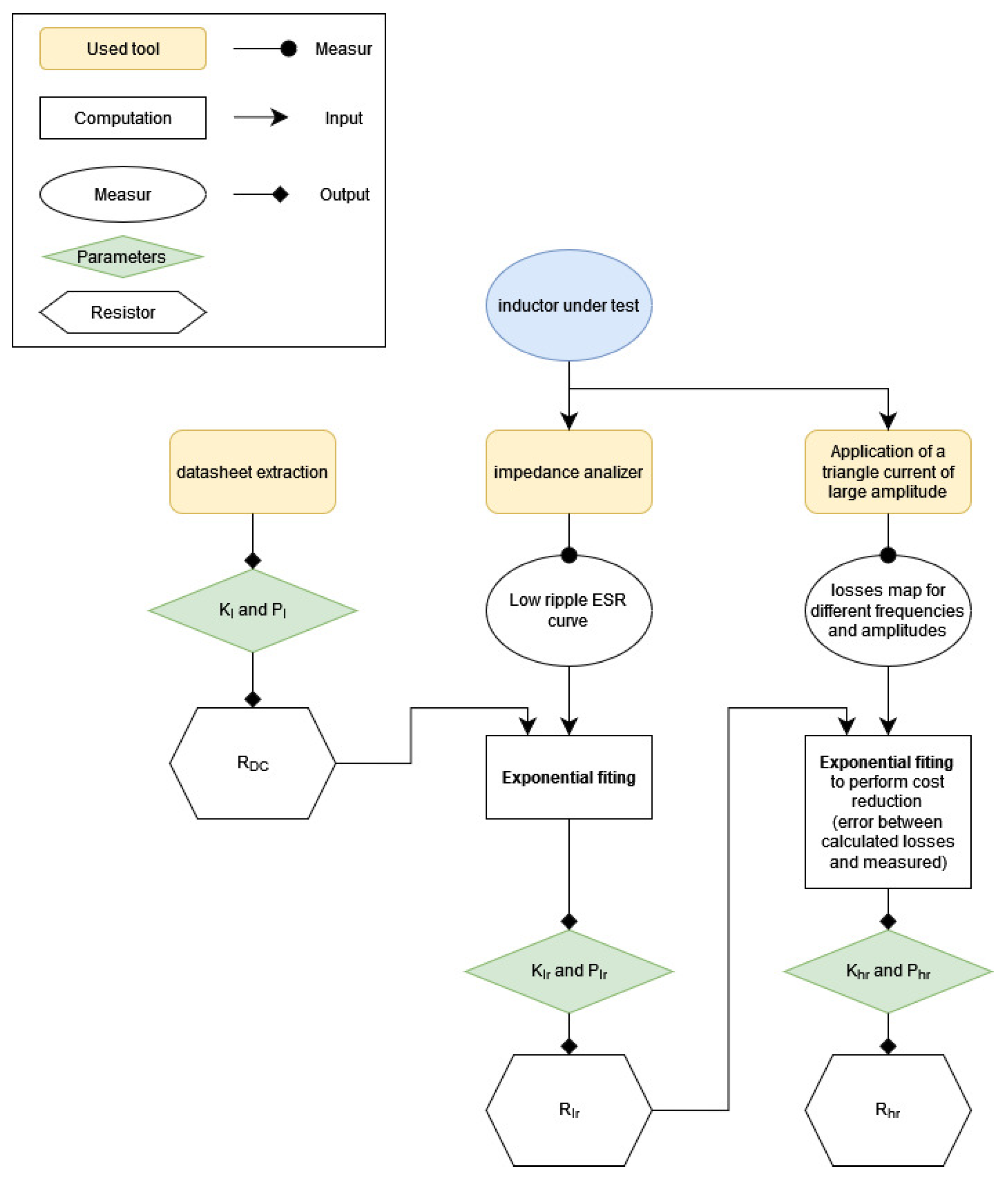
Figure 5.
Characterization and modelling approach to derive the generic mathematical inductor losses model and corresponding parameters with respect to inductor value.
Figure 5.
Characterization and modelling approach to derive the generic mathematical inductor losses model and corresponding parameters with respect to inductor value.
Figure 6.
Evolution of the series resistance of the MSS1210-473 47 µH inductor with respect to frequency. Practical characterization in blue and equivalent model in dashed red.
Figure 6.
Evolution of the series resistance of the MSS1210-473 47 µH inductor with respect to frequency. Practical characterization in blue and equivalent model in dashed red.
Figure 7.
Bench topology for the inductor AC losses measurement under high ripple current and variable frequency. (Left) the schematic, (Right) the low voltage “high” current full-bridge inverter (30 V up to 5 A).
Figure 7.
Bench topology for the inductor AC losses measurement under high ripple current and variable frequency. (Left) the schematic, (Right) the low voltage “high” current full-bridge inverter (30 V up to 5 A).
Figure 8.
(a) Evolution of the power losses in the inductor under test for a frequency range from 50 kHz to 150 kHz. Left, comparison of the losses between the AC losses measure and the model described with Equation (5). Right comparison of the losses between the measure and the model described in Equation (7). (b) Equivalent impedance model of the inductor under test.
Figure 9.
Evolution of losses into an MSS1210-473 47 µH inductor at 100 kHz over a ripple current magnitude from 0.2 up to 2 A. The upper curve represents the losses into the inductor measured and calculated with models of Equation (4) in blue and (6) in red. The bottom curves present the absolute relative errors between the impedance analyser model and the AC loss model.
Figure 10.
Evolution of the losses produced by three inductors under test. Validation of the + + model.
Figure 10.
Evolution of the losses produced by three inductors under test. Validation of the + + model.
Figure 11.
of the transistor SIS862DN-T1-GE3 versus Drain-source Voltage from Equation (12) in red and from component datasheet [
25] in bleu.
Figure 11.
of the transistor SIS862DN-T1-GE3 versus Drain-source Voltage from Equation (12) in red and from component datasheet [
25] in bleu.
Figure 12.
Schematic of a VSI + its differential mode input filter for conducted EMI compliance + the LISN resistors (LISN simplified representation in high frequency range).
Figure 12.
Schematic of a VSI + its differential mode input filter for conducted EMI compliance + the LISN resistors (LISN simplified representation in high frequency range).
Figure 13.
Frequency domain representation of 1A magnitude at 83% duty cycle filtered by a capacitor of 40 µF or by a filter ( = 20 µF, = 3 µH, = 20 µF) to meet the 60 dBµV limits using Equation (15) to calculate the value of .
Figure 13.
Frequency domain representation of 1A magnitude at 83% duty cycle filtered by a capacitor of 40 µF or by a filter ( = 20 µF, = 3 µH, = 20 µF) to meet the 60 dBµV limits using Equation (15) to calculate the value of .
Figure 14.
Ceramic capacitor equivalent series resistance with respect to frequency. (Left), manufacturer data, (right), equivalent model representation for the series resistance with respect to frequency.
Figure 14.
Ceramic capacitor equivalent series resistance with respect to frequency. (Left), manufacturer data, (right), equivalent model representation for the series resistance with respect to frequency.
Figure 15.
Inductor losses calculated for the two MSS1210 inductors of bidirectional full bridge converter working under 30 V input with 20 V output at 2.5 A.
Figure 15.
Inductor losses calculated for the two MSS1210 inductors of bidirectional full bridge converter working under 30 V input with 20 V output at 2.5 A.
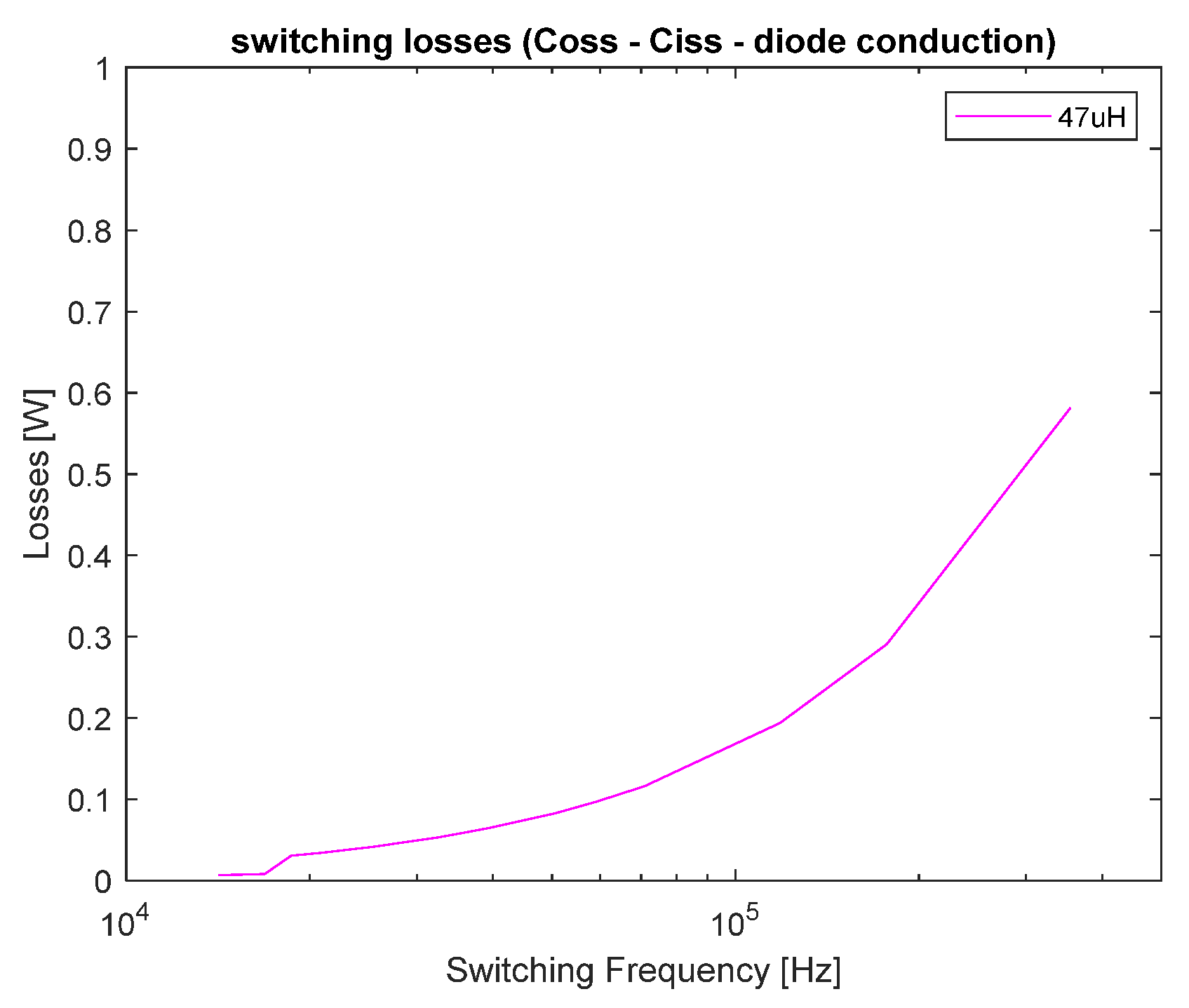
Figure 16.
Switching losses made by the four transistors depending on the switching frequency in a converter using two 47 uH main inductors.
Figure 16.
Switching losses made by the four transistors depending on the switching frequency in a converter using two 47 uH main inductors.
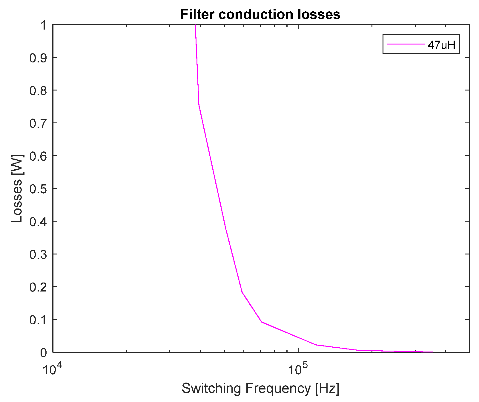
Figure 17.
Losses caused by the two filtering inductors depending on the switching frequency in a converter which 2 × 47 µH main inductors.
Figure 17.
Losses caused by the two filtering inductors depending on the switching frequency in a converter which 2 × 47 µH main inductors.
Figure 18.
Calculated total losses into the full-bridge converter considering all losses modelled in
Section 3. These losses are considered for a 30 V to 20 V, 50 W converter equipped with 2 × 47 µH main inductors.
Figure 18.
Calculated total losses into the full-bridge converter considering all losses modelled in
Section 3. These losses are considered for a 30 V to 20 V, 50 W converter equipped with 2 × 47 µH main inductors.
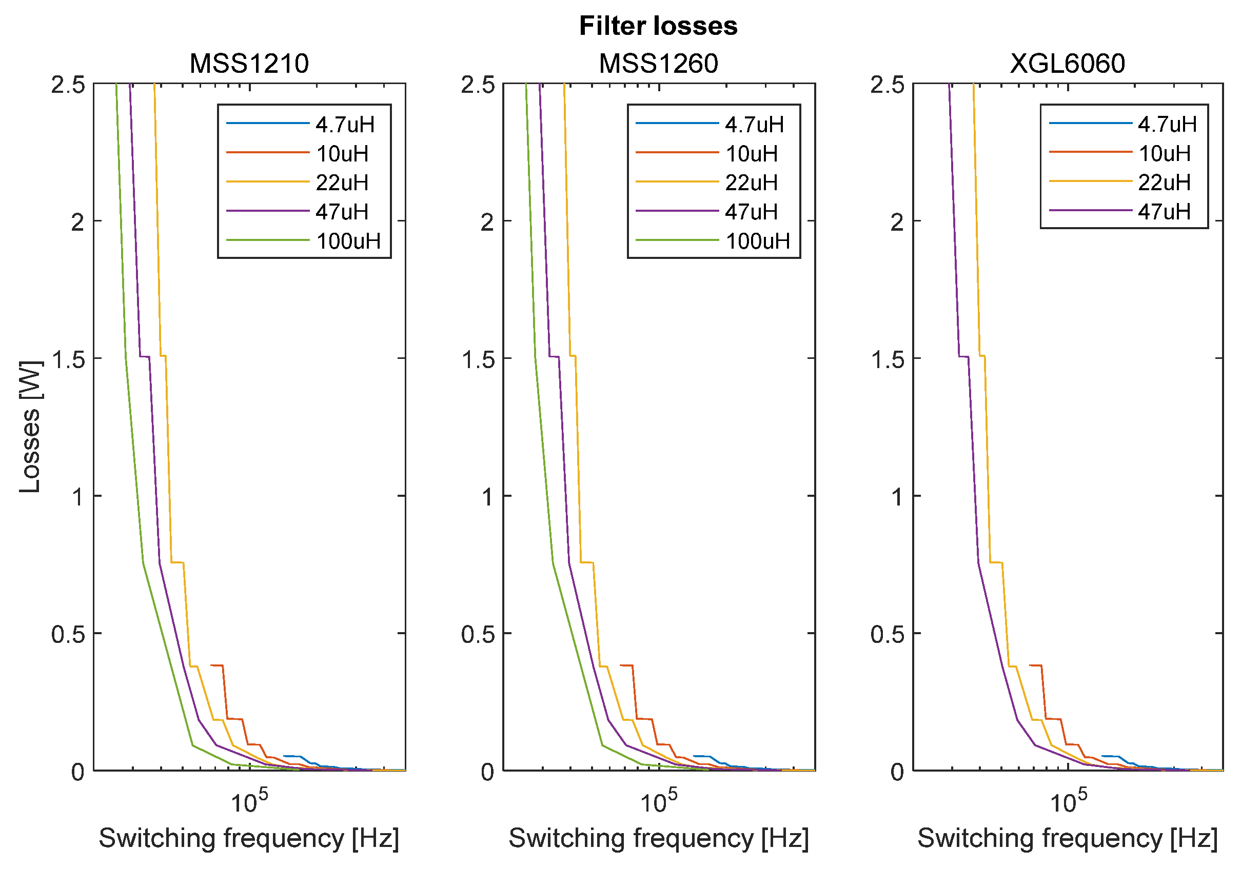
Figure 19.
Losses into the main inductors, for multiple inductor values in the three series.
Figure 19.
Losses into the main inductors, for multiple inductor values in the three series.
Figure 20.
Active device switching losses for a 50 W–30 V to 20 V converter with respect to the main inductor value and the switching frequency.
Figure 20.
Active device switching losses for a 50 W–30 V to 20 V converter with respect to the main inductor value and the switching frequency.
Figure 21.
Losses in the output filter depending on the main inductor values (coloured curves) with respect to the switching frequency. The filtering inductor values are the minimum discrete standard values complying with the 60 dBµV limits at LSIN resistors as proposed in
Section 4.1.
Figure 21.
Losses in the output filter depending on the main inductor values (coloured curves) with respect to the switching frequency. The filtering inductor values are the minimum discrete standard values complying with the 60 dBµV limits at LSIN resistors as proposed in
Section 4.1.
Figure 22.
Total mosses modelling results for the three inductor families. Total losses are represented as a function of the switching frequency and the inductor values.
Figure 22.
Total mosses modelling results for the three inductor families. Total losses are represented as a function of the switching frequency and the inductor values.
Figure 23.
Model results for the three inductor families. Total losses are represented as a function of the Current Ripple and the inductor values.
Figure 23.
Model results for the three inductor families. Total losses are represented as a function of the Current Ripple and the inductor values.
Figure 24.
Maximum losses allowed in the inductor for various inductor values and for two temperature rises. Data extracted from datasheets [
15,
16,
17].
Figure 24.
Maximum losses allowed in the inductor for various inductor values and for two temperature rises. Data extracted from datasheets [
15,
16,
17].
Figure 25.
Schematic of the opposition method to characterize converter losses.
Figure 25.
Schematic of the opposition method to characterize converter losses.
Figure 26.
Picture of the test bench with the two TI controllers, one for each converter and in between the two converters, one feeding the other.
Figure 26.
Picture of the test bench with the two TI controllers, one for each converter and in between the two converters, one feeding the other.
Figure 27.
Optimization results compared with experimental measurements (curves with circles). For one converter processing, 50 W from 30 V to 20 V. Measure are carried out with back-to-back method. The results are plotted with respect to current ripples into the main inductors.
Figure 27.
Optimization results compared with experimental measurements (curves with circles). For one converter processing, 50 W from 30 V to 20 V. Measure are carried out with back-to-back method. The results are plotted with respect to current ripples into the main inductors.
Figure 28.
Optimization results compared with experimental measurements (curves with circles). For one converter processing, 20 W from 30 V to 20 V. Measures are carried out with the back-to-back method. The results are plotted with respect to the current ripple magnitude into the main inductors.
Figure 28.
Optimization results compared with experimental measurements (curves with circles). For one converter processing, 20 W from 30 V to 20 V. Measures are carried out with the back-to-back method. The results are plotted with respect to the current ripple magnitude into the main inductors.
Table 1.
The main characteristics of the three inductor series considered in this work [
15,
16,
17].
Table 1.
The main characteristics of the three inductor series considered in this work [
15,
16,
17].
| Manufacturer Reference | Volume (mm3) | Weight (g) | Inductor Value Range (µH) | DC Resistor Range (mΩ) | Frequency Range (MHz) |
|---|
| MSS1210 | 1353 | 5.1–6.2 | 10–10,000 | 14–7390 | 4–0.2 |
| MSS1260 | 777 | 2.8–3.3 | 1–1000 | 5.8–1295 | >10–0.6 |
| XGL6060 | 274 | 1.41–1.56 | 0.22–47 | 1.1–97 | 50–2 |
Table 2.
Series resistance model parameters for the three manufacturer inductor series.
Table 2.
Series resistance model parameters for the three manufacturer inductor series.
| Inductor Series | Factor | MSS1210 | MSS1260 | XGL6060 |
|---|
| 1 | 1353 | 777 | 274 |
| | 1 | 430 | 700 | 710 |
| 1 | 0.915 | 0.915 | 0.915 |
| | 1 × 10⁻³ | 210 | 88 | 0.3 |
| 1 | 1.5 | 1.55 | 1.9 |
| | 1 | 67 | 45 | 134 |
| 1 | 1.049 | 1.089 | 1.028 |
Table 3.
Energies lost at each commutation due to , and body diode conduction.
Table 3.
Energies lost at each commutation due to , and body diode conduction.
| Parasitic Capacitor | | Ciss | Transistor Body Diode |
|---|
| Voltage | 30 V | 6.5 V | 0.7 V |
| Stored energy | 287 nJ | 81 nJ | nJ |
Table 4.
Calculated losses at global optimums for each series and individual main inductor losses at these optimums.
Table 4.
Calculated losses at global optimums for each series and individual main inductor losses at these optimums.
| Serie | MSS1210 | MSS1260 | XGL6060 |
|---|
Optimal
total losses | 1.38 W | 1.44 W | 1.28 W |
Main
inductor losses | 2 × 0.37 W | 2 × 0.40 W | 2 × 0.32 W |
Table 5.
Median thermal resistance of copper to the core in MSS1210, MSS1260 and XGL6060 series.
Table 5.
Median thermal resistance of copper to the core in MSS1210, MSS1260 and XGL6060 series.
| Series | MSS1210 | MSS1260 | MSS6060 |
|---|
| (°C/W) at +20° | 75 | 79 | 26 |
| (°C/W) at +40° | 80 | 83 | 29 |
Table 6.
Thermal rising of a 22 µH selected during optimization process of the 50 W converter.
Table 6.
Thermal rising of a 22 µH selected during optimization process of the 50 W converter.
| Series | MSS1210 | MSS1260 | MSS6060 |
|---|
| Inductor losses (W) | 0.37 | 0.40 | 0.32 |
| Thermal rising (°C) | 27.8 to 29.6 | 31.6 to 33.2 | 8.3 to 9.3 |


