Article

Two-Terminal Electronic Circuits with Controllable Linear NDR Region and Their Applications

1
Department of Electronics, Robotics, Monitoring and IoT Technologies, National Aviation University, 03058 Kyiv, Ukraine
2
Projects and Maintenance Section, The Private Department of the President of the United Arab Emirates, Abu Dhabi P.O. Box 372, United Arab Emirates
3
Enavate, 01601 Kyiv, Ukraine
*
Author to whom correspondence should be addressed.
Appl. Sci. 2021, 11(21), 9815; https://doi.org/10.3390/app11219815
Submission received: 16 August 2021 / Revised: 9 October 2021 / Accepted: 16 October 2021 / Published: 20 October 2021

Abstract

:
Negative differential resistance (NDR) is inherent in many electronic devices, in which, over a specific voltage range, the current decreases with increasing voltage. Semiconductor structures with NDR have several unique properties that stimulate the search for technological and circuitry solutions in developing new semiconductor devices and circuits experiencing NDR features. This study considers two-terminal NDR electronic circuits based on multiple-output current mirrors, such as cascode, Wilson, and improved Wilson, combined with a field-effect transistor. The undoubted advantages of the proposed electronic circuits are the linearity of the current-voltage characteristics in the NDR region and the ability to regulate the value of negative resistance by changing the number of mirrored current sources. We derive equations for each proposed circuit to calculate the NDR region’s total current and differential resistance. We consider applications of NDR circuits for designing microwave single frequency oscillators and voltage-controlled oscillators. The problem of choosing the optimal oscillator topology is examined. We show that the designed oscillators based on NDR circuits with Wilson and improved Wilson multiple-output current mirrors have high efficiency and extremely low phase noise. For a single frequency oscillator consuming 33.9 mW, the phase noise is −154.6 dBc/Hz at a 100 kHz offset from a 1.310 GHz carrier. The resulting figure of merit is −221.6 dBc/Hz. The implemented oscillator prototype confirms the theoretical achievements.

1. Introduction

Negative differential resistance is a property of nonlinear semiconductor devices or special electronic circuits. An increase in the voltage drop across them results in a decrease in the flowing current.
Electronic devices with NDR are widely used in electronic and radio engineering systems of the broadest use, not only as of the main elements of amplifying [1], oscillating [2,3], multiplexing [4], static-random-access-memory (SRAM) [5], and switching circuits [6]. Recently, very promising is the use of NDR devices in radar [7], communication [8] and info-communication [9] circuits, analog-to-digital converters [10], and neural network circuits [11] due to the significant simplification of many circuitry solutions. Other possible applications of NDR devices can be found in the comprehensive overview by Reference [12].
Generally, we can divide NDR devices into N and Λ current-voltage characteristics devices and S characteristics devices. Since the article’s main content is N-type NDR devices, we will analyze previously published studies for electronic structures with N- and Λ-type characteristics.
One of the main characteristics of any NDR circuit is the peak-to-valley current ratio (PVCR), which is the ratio of the peak to the valley current. In many practical tasks, it is necessary to be able to control the PVCR. For example, in oscillators, the PVCR determines the slope of the current-voltage characteristic in the NDR region, hence the value of the differential resistance at the operating point. In turn, the self-excitation of the oscillator depends on the value of the differential resistance.
The literature review (see Section 2) shows that it is impossible to control PVCR in the NDR circuits of most published studies. In studies where it is possible, the maximum current level lies in the nA or µA range.
This study proposes new two-terminal NDR circuits that combine a field-effect transistor (FET) with a multiple-output cascode, Wilson, or improved Wilson current mirror (CM). Possible types of FETs include a junction field-effect transistor (JFET), metal-semiconductor field-effect transistor (MESFET), high-electron-mobility transistor (HEMT), or pseudomorphic high-electron-mobility transistor (PHEMT). In the analyzed circuits, we control PVCR by changing the number of mirrored currents. Here, we show that one could set the PVCR to any desired value. There are several advantages of the proposed method of controlling PVCR. Firstly, the power supply voltage keeps constant. Secondly, the peak point and valley point voltages are not changed with increasing the number of mirrored currents. Thirdly, the types of transistors are also not changed. Fourthly, the current-voltage characteristics in the NDR region are almost linear. Fifthly, the output resistance of the CM is exceptionally high, which is a valuable property for oscillator applications. The mathematical modeling of the total current in the NDR region has been conducted for all NDR circuits using JFET and PHEMT as a FET for Shockley and Curtice drain current equations. We consider the applications of the proposed NDR circuits for microwave oscillators and voltage-controlled oscillators (VCOs).
The simulation results show that the circuit with multiple-output improved Wilson CM (MIWCM) has the highest slope of the current-voltage curve in the NDR region. The oscillators built on the proposed NDR circuits have extremely low phase noise and are superior in efficiency to most oscillators. The microwave oscillator with multiple-output Wilson CM (MWCM) has the lowest phase noise and the best figure of merit (FOM) when the load is 50 Ω. The VCO with MIWCM has the best FOM.

2. Review

N- and Λ-type characteristics can be obtained both through special semiconductor devices and electronic circuits. Let us consider the most prominent studies related to both groups of NDR structures. Esaki [13,14] and Gunn [15] were the pioneers of N-type NDR devices developing the tunnel and Gunn diodes, respectively, in 1957 and 1962. Stanley and Ager [16] proposed a two-terminal N-type NDR circuit based on one JFET and one bipolar junction transistor (BJT). Sharma and Dutta Roy [17] considered a versatile N-type NDR circuit comprising two BJTs and four resistors. One resistor can control the slope of the current-voltage characteristics in the NDR region. Chung Wu and Ching Wu [18] developed a theory of FET-like NDR devices. The proposed NDR devices include two or three FETs. Some circuits also comprise one BJT. Chua et al. [19] considered several NDR circuits based on the special connection of BJT, JFET, and metal-oxide-semiconductor FET (MOSFET). The authors developed an algorithm to generate a device with N-type current-voltage characteristics. Chen et al. [5] considered the NDR structure of the source-coupled n-channel metal-oxide-semiconductor (nMOS) and p-channel metal-oxide-semiconductor (pMOS) transistors exhibiting ultrahigh PVCR. Such a device can be a building element of SRAM. Trajković and Willson [20] considered two-terminal circuits with N-type current-voltage characteristics using a special connection of two BJTs and three resistors. Jung et al. [21] reported fabricating an N-type double-NDR device using a 3D hybrid structure that includes two 2D vdW/organic heterojunctions and one organic resistor. Kobashi et al. [22] proposed a new NDR transistor based on a p-n heterojunction of organic semiconductors with well-balanced carrier transport through the junction. Lv et al. [23] reported tunneling FET (TFET) based on a BP/InSe heterostructure in contact with graphene electrodes and covered with an hBN layer. In TFET, the tunneling current and the NDR region strongly depend on electrostatic gating. Qiu et al. [24] considered a graphene-based NDR device based on intrinsic armchair-edged nanoribbons with uniform widths. The device provides a sharp current peak of 1.2 μA at bias 0.8 V and a PVCR of 2.7. Kheirabadi et al. [25] considered armchair graphene nanoribbons for creating the NDR effect, which could have applications in nanoelectronics and nanosensors. Yang and Hwu [26] analyzed the tunable NDR characteristics of metal-insulator-semiconductor-insulator-metal tunnel diodes structure where the PVCR can be over 100. The NDR voltage interval exceeds 1 V. Xiong et al. [27] reported a four-terminal NDR device made from a 2D BP/Al2O3/BP sandwich structure with the PVCR exceeding 100 at room temperature. Kim et al. [28] considered an m-NDR device based on a BP/(ReS2 + HfS2) type-III double-heterostructure and its application to a ternary latch circuit capable of storing three logic states. Liang et al. [29] proposed a Λ-type NDR circuit based on a particular connection of three nMOS transistors with the same length and different widths of the channel. Gan et al. [30] considered a MOS-heterojunction bipolar transistor (HBT) N-type NDR circuit based on three n-channel MOS and one SiGe HBT device with two power supplies. At specific supply voltages, the NDR circuit provides the PVCR of about 8. Chung et al. [31] reported a three-terminal Si-based NDR device by epitaxially growing a resonant interband tunnel diode atop the emitter of a Si/SiGe HBT on a silicon substrate. The device provides an adjustable PVCR. Semenov [32] proposed a Λ-type NDR BJT-metal–oxide–semiconductor FET (MOSFET) circuit applied to periodic and chaotic mode oscillators. Gan et al. [33] considered a novel NDR circuit comprising nMOS transistors and HBT with application to inverter design based on 0.35 µm SiGe technology. Ulansky et al. [34] presented five electronic circuits of NDR VCOs based on a GaAs transistor and single-output BJT CM. Ulansky et al. [35] considered an NDR circuit comprising a FET and a simple BJT CM with multiple outputs that control the slope of the current-voltage curve by changing the number of CM outputs. Yang [36] investigated a resonant tunneling electronic circuit with reactance elements having high and multiple peak-to-valley current density ratios displayed in the NDR curve. Kadioglu [37] considered a monolayer structure based on vanadium phosphide with a current-voltage characteristic having the NDR region. Rathi et al. [38] observed an NDR region in the current-voltage curve in graphene oxide two-terminal device with precise control of carbon-oxygen ratio. The fabricated novel electronic device can find application in switches and oscillators. Sharma et al. [39] synthesized graphene oxide quantum dots based on graphene oxide, cysteine, and H2O2 having N-type current-voltage characteristics with PVCR of 4.7. Shim et al. [40] demonstrated an NDR device on the base of a phosphorene/rhenium disulfide (BP/ReS2) heterojunction. It has a high PVCR of 4.2 at room temperature. The peak and valley currents are 3 and 0.7 nA, respectively.
We can draw the following conclusions from the review of published studies:
  • Considerable attention is paid to developing new NDR devices [21,22,23,24,25,26,27,28,30,31,33,36,37,38,39], indicating the research topic’s relevance.
  • Most NDR devices and circuits use one, two, or even three power supplies. Such devices have two [14,15,16,17,18,19,20,34,35,38,39], three [18,29,31,32,33], or four [27] terminals.
  • In most of the published studies, there is no possibility of controlling the PVCR. The PVCR control is available in the NDR devices considered in the studies [26,27,31,39], but the maximum current levels are in the nA and µA ranges. In the NDR circuit [17], the control of PVCR is possible in the mA range by changing the value of one of the resistors.

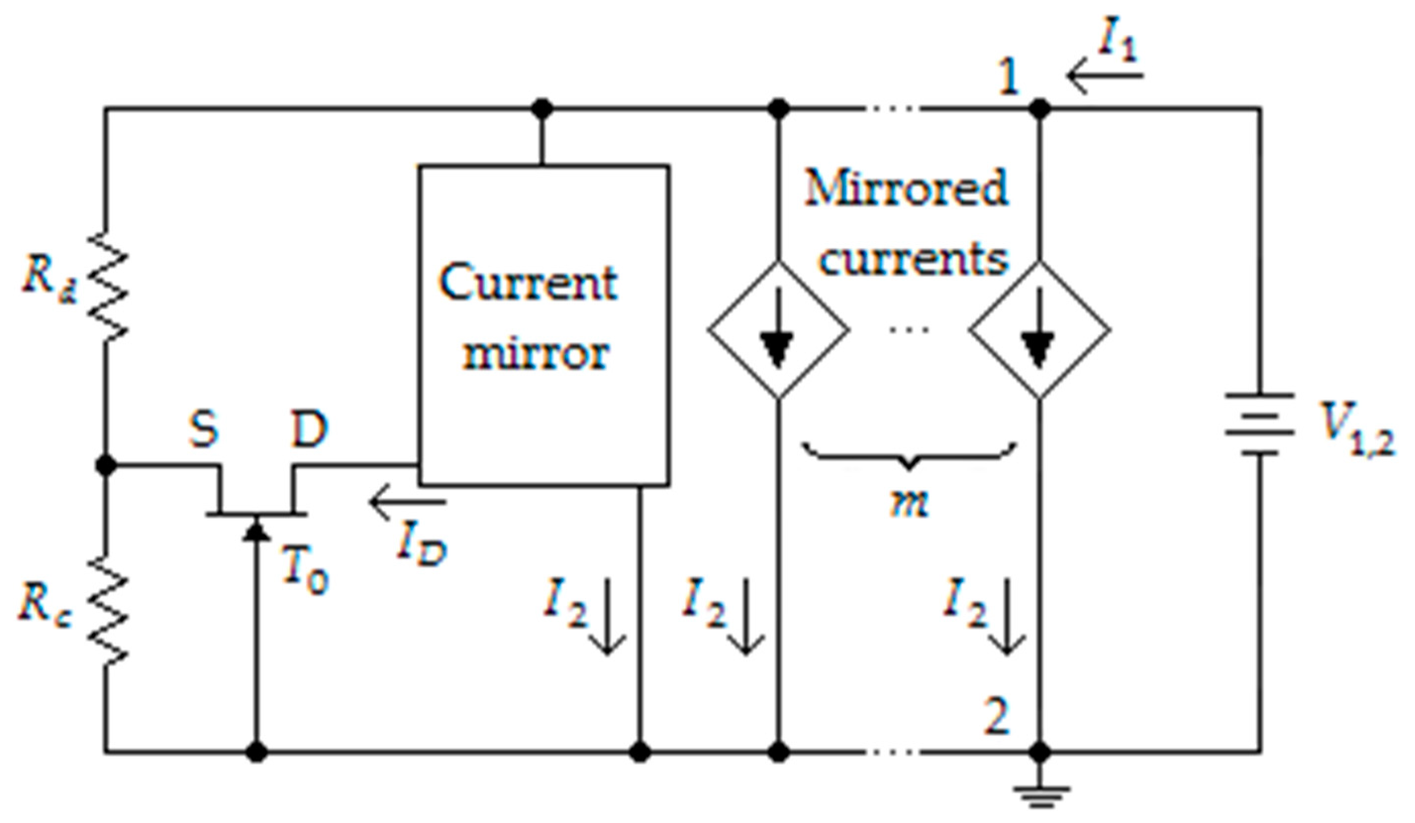
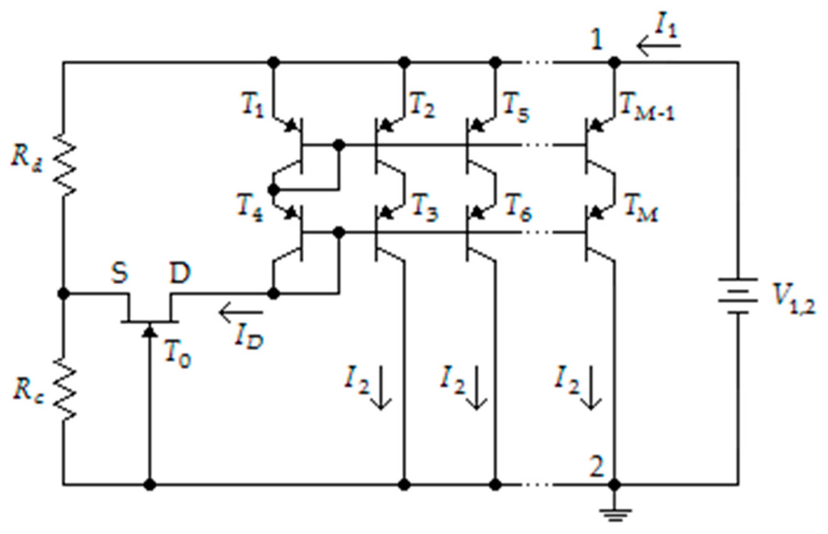
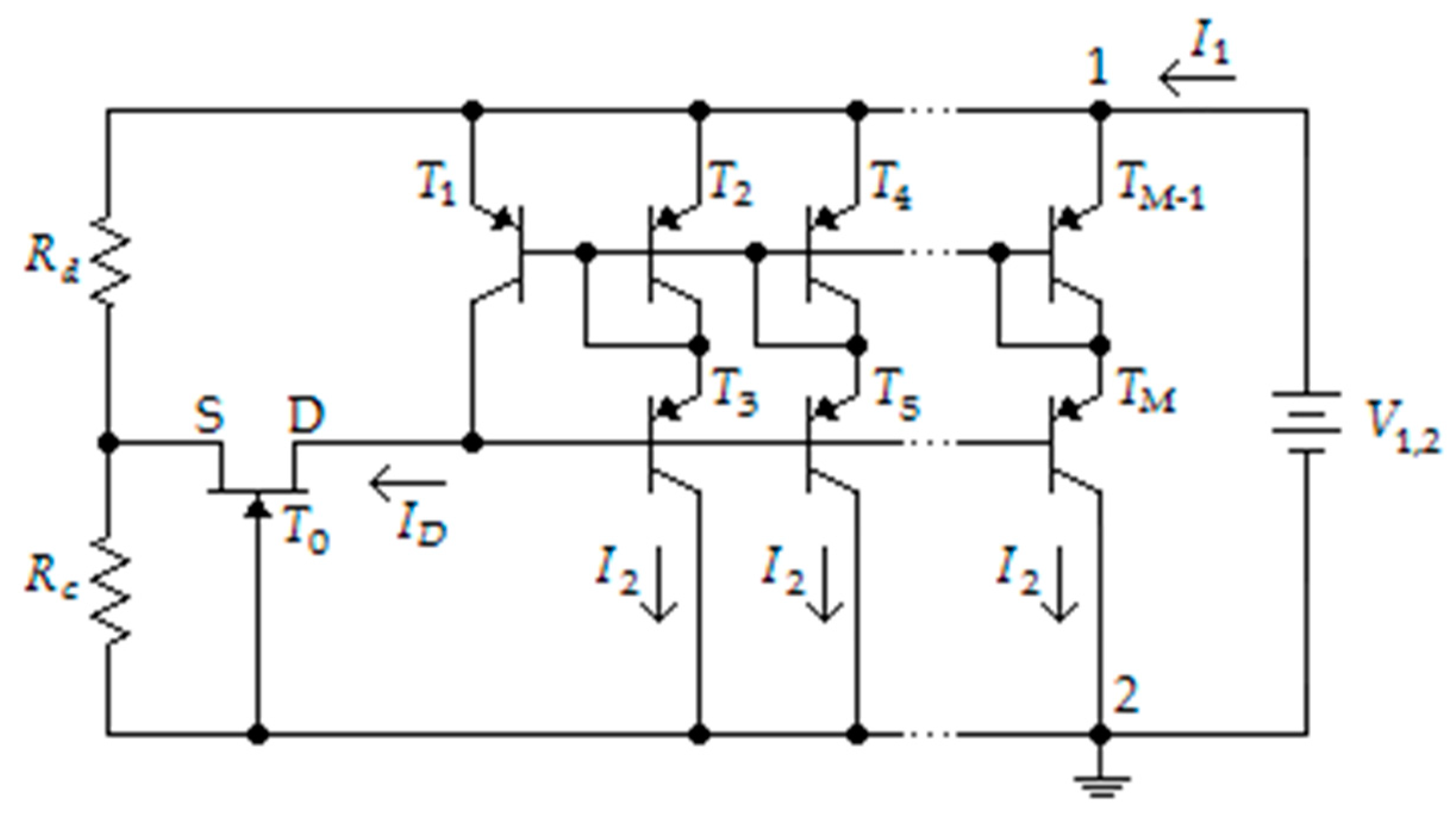
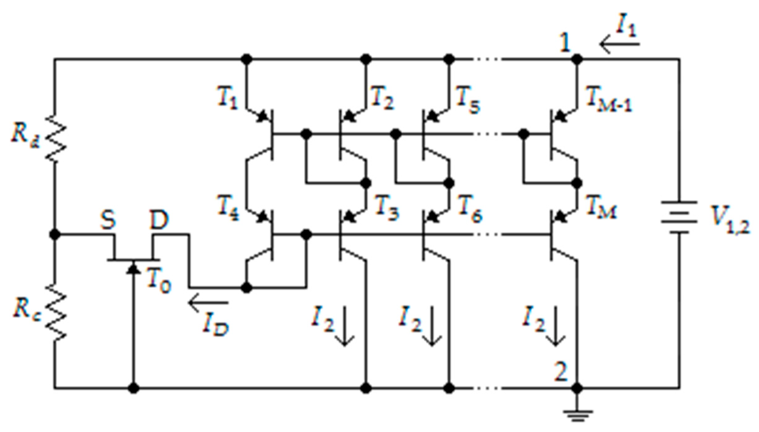
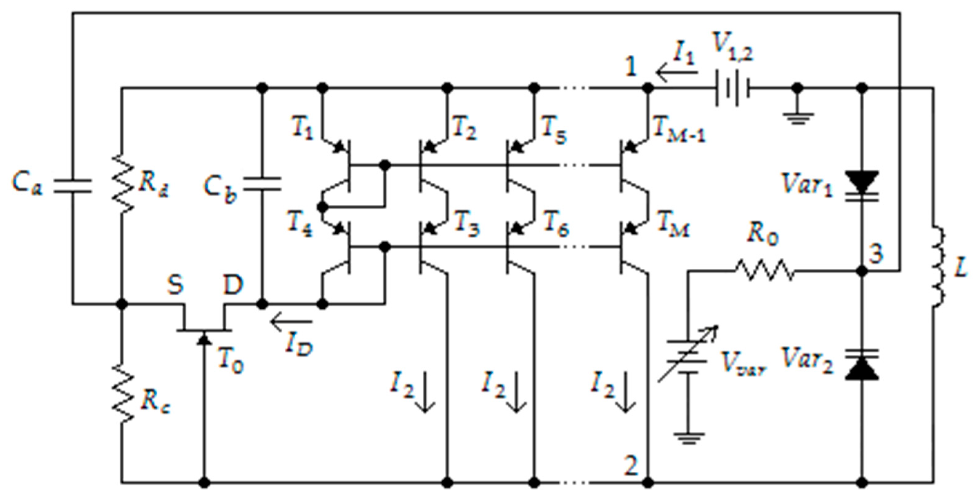
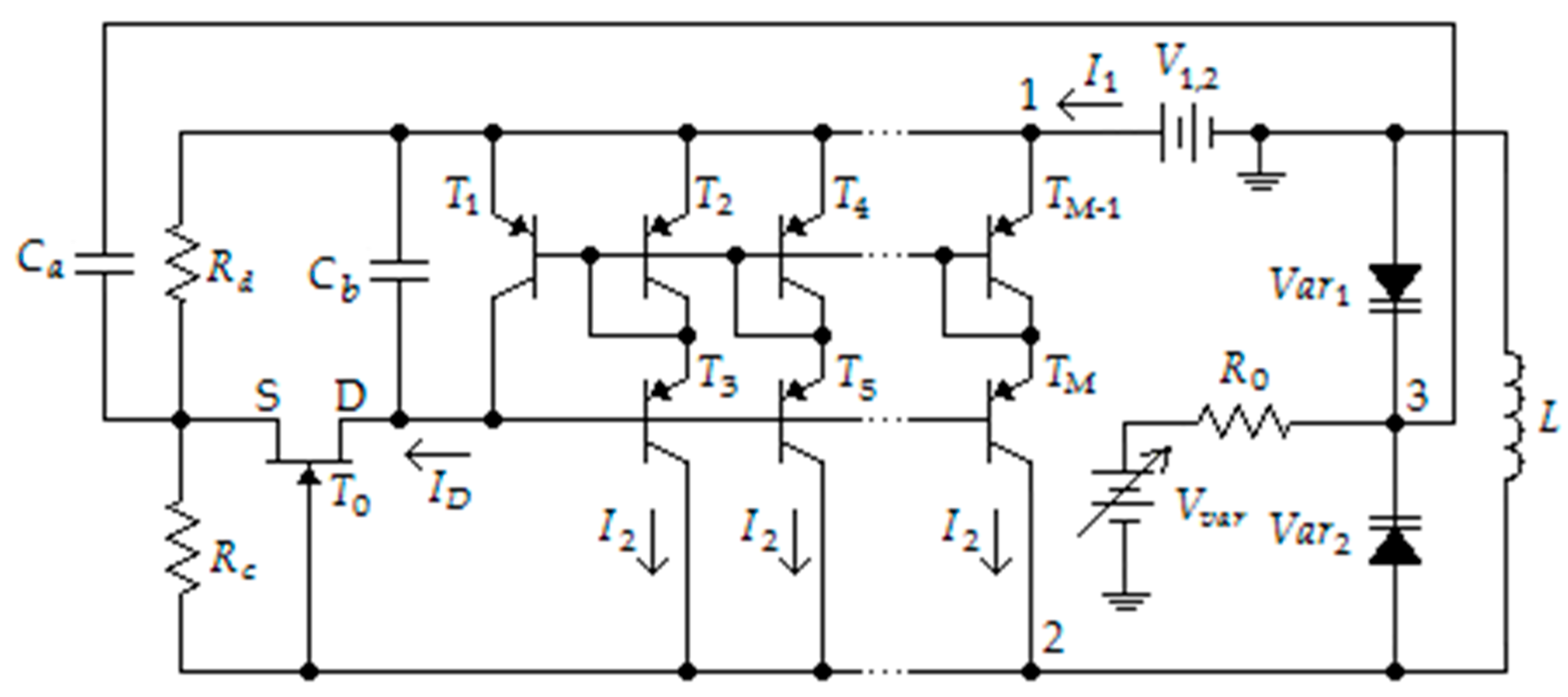
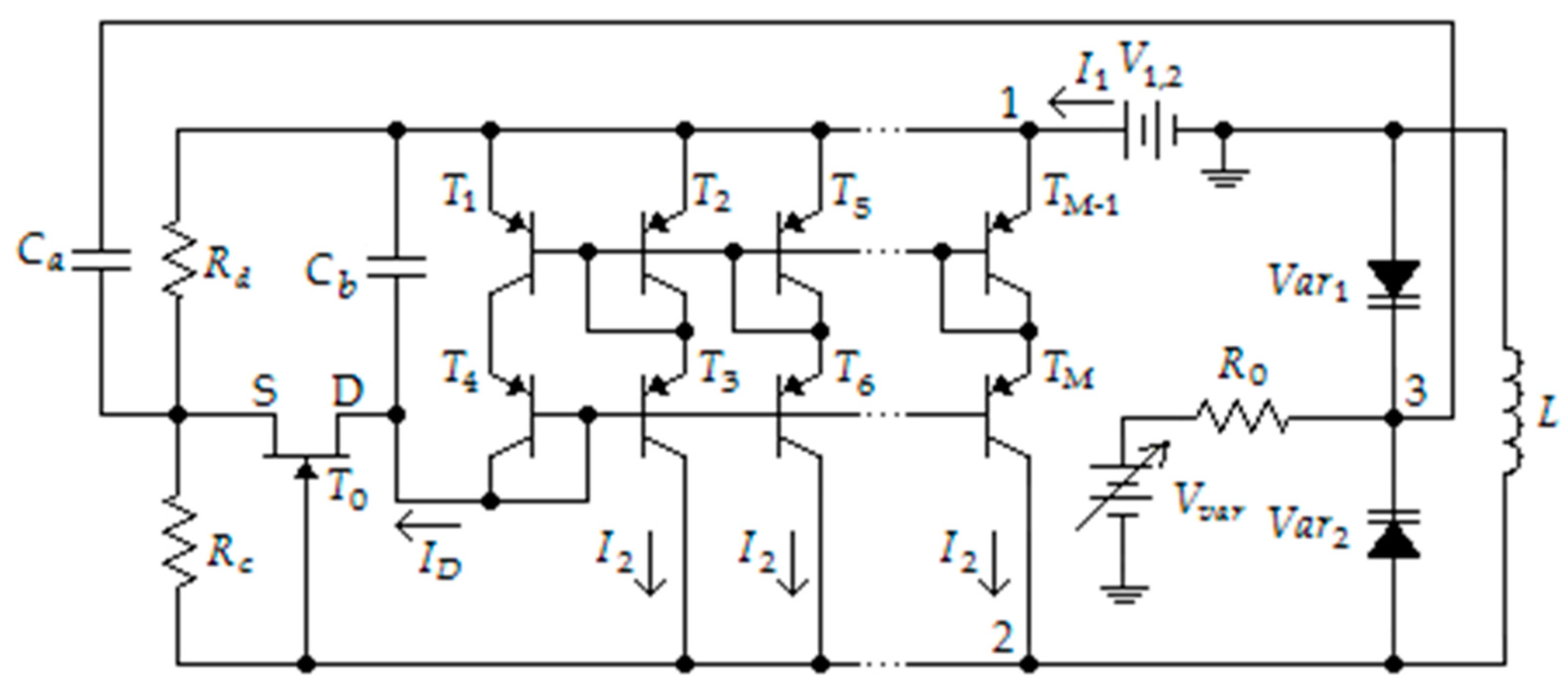
3. Two-Terminal NDR Circuits

Figure 1 shows a two-terminal electronic circuit with a controllable NDR region. The circuit comprises a voltage divider Rc, Rd, an n-channel FET T0, a current mirror with m (m = 0, 1, 2,…) additional outputs (mirrored current sources), and a power supply V1,2.
The circuit of Figure 1 has N-type current-voltage characteristics between nodes 1 and 2, as shown in Figure 2. The slope of the NDR region in the current-voltage characteristics depends on the number (m) of the additional mirrored current sources I2. In Figure 2, the green curve corresponds to m = 0, the blue curve to m = 1, and the red curve to m = 2. As seen in Figure 2, the current-voltage characteristics have four regions. In the first (0, VX) and fourth (VZ, ∞) regions, the current I1 depends only on the voltage V1,2. In these regions, all transistors are off. In the second region (VX, VY), all transistors are on. Transistor T0 operates in the ohmic region, and current I1 increases. We should also note that the voltage VY does not depend on the value of m, i.e., VYi = VY, i = 0, 1,…, m. In the third region (VY, VZ), transistor T0 operates in the saturation region and current I1 decreases due to a decrease in the gate-source voltage.
The current I1 consists of two currents in the NDR region: the current through resistor Rc and m + 1 currents I2. The current through resistor Rc is due to power supply V1,2 and the drain-current ID of transistor T0. Thus, the current I1 is given by
I 1 = ( m + 1 ) I 2 + I D R d R c + R d + V 1 , 2 R c + R d .
Outside the region (VX, VZ), the current I1 is only due to the power supply voltage V1,2.
Further, we assume the matching of all transistors in the multiple-output CMs. As is well-known [40], for large transistor dc gain hFE, the currents I2 and ID are approximately identical. The magnitude of the difference in currents I2 and ID depends on the selected CM.
Figure 3 shows a two-terminal NDR circuit with the multiple-output cascode CM (MCCM). The following relation links currents I2 and ID [41]:
I 2 = I D ( 1 4 h F E + 2 h F E 2 + 4 h F E + 2 ) .
By substitution (2) to (1), we obtain the total current in the NDR region:
I 1 = I D [ ( m + 1 ) 1 + 4 / h F E + 2 / h F E 2 + R d R c + R d ] + V 1 , 2 R c + R d .
The advantage of using cascode CM in the two-terminal NDR circuit is its high output resistance. The disadvantage is a mismatch between currents I2 and ID.
Figure 4 shows a two-terminal NDR circuit using MWCM. With finite Early voltage VA, the currents I2 and ID are related as follows [41]:
I 2 = I D ( 1 2 h F E 2 + 2 h F E + 2 ) ( 1 V E B 3 V A ) ,
where VEB3 is the emitter-base voltage of transistor T3.
Substituting (4) to (1) gives the following equation for the total current in the NDR region:
I 1 = I D [ ( m + 1 ) ( 1 2 h F E 2 + 2 h F E + 2 ) ( 1 V E B 3 V A ) + R d R c + R d ] + V 1 , 2 R c + R d .
The advantage of using MWCM in the NDR circuit of Figure 1 is high output resistance and a slight mismatch between master branch current (ID) and slave branch current (I2). The disadvantage is the difference in collector-emitter voltages VEC1 and VEC2, which is equal to voltage VEB3.
Figure 5 shows a two-terminal NDR circuit with MIWCM. The improved Wilson CM introduces a diode-connected transistor T4 equalizing the collector-emitter voltages of transistors T1 and T2. Therefore, Equation (4) is reduced to [41]
I 2 = I D ( 1 2 h F E 2 + 2 h F E + 2 ) .
Substituting (6) to (1), we obtain an equation for the total current in the NDR region:
I 1 = I D [ ( m + 1 ) ( 1 2 h F E 2 + 2 h F E + 2 ) + R d R c + R d ] + V 1 , 2 R c + R d .
Analysis of (3), (5), and (7) shows that the total current I1 in the NDR region is a function of the drain current of transistor T0, which is an n-channel FET. For the existence of the NDR region, the transistor T0 must have a negative threshold voltage. Therefore, suitable types of transistors are JFET, depletion metal-oxide-semiconductor FET (DMOSFET), MESFET, HEMT, and PHEMT. As shown in Reference [35], the two-terminal NDR circuit with a multiple-output simple CM has an NDR effect when transistor T0 is in saturation mode. In the circuits presented by Figure 3, Figure 4 and Figure 5, transistor T0 should also operate in the saturation mode in the NDR region. Thus, to calculate the current I1, it is necessary to model the current ID for the selected type of transistor T0.

4. Modeling the Drain Current of Transistor T0

As we can see from (3), (5), and (7), to calculate the total current I1 in the NDR region, we should know the drain current ID of the transistor T0. The modeling of current ID depends on the type of transistor T0.
If transistor T0 is a JFET, the Shockley equation well represents the drain current in the saturation region:
I D = I D S S V P 2 ( V P V G S ) 2 ,
where IDSS is the drain current of transistor T0 at zero bias, VP is the negative pinch-off voltage, and VGS is the gate-source voltage.
The voltage between gate and source of transistor T0 is negative and consists of two parts: the voltage due to voltage divider Rc, Rd:
R c V 1 , 2 R c + R d ,
and the voltage drop across resistor Rc because of the current through this resistor, i.e.,
I D R d R c + R d R c .
Combining (9) and (10) gives
V G S = R c V 1 , 2 R c + R d I D ( R c R d ) .
Substituting (11) to (8) and providing some mathematical manipulations, we obtain the following quadratic equation for determining the value of the current ID:
( R c R d ) 2 I D 2 + [ 2 ( V P + V 1 , 2 R c R c + R d ) ( R c R d ) V P 2 I D S S ] I D + ( V P + V 1 , 2 R c R c + R d ) 2 = 0 .
If transistor T0 is a MESFET, we can model the current ID by one of the nonlinear large-signal models [42,43,44]. For example, the popular Curtice model in the saturation region is as follows [42]:
I D = b ( V G S V T H ) 2 ( 1 + λ V D S ) tanh ( α V D S ) ,
where b is the transconductance, λ is the channel length modulation coefficient, α is the coefficient of the hyperbolic tangent function, VDS is the drain-source voltage, and VTH is the threshold voltage.
The voltage VDS we find by applying Kirchhoff’s voltage law to the circuit of Figure 1.
V 1 , 2 ( V 1 , 2 V D ) V D S + V G S = 0 ,
where VD is the voltage at the drain of transistor T0.
Substituting VGS from (11) into (14), we obtain
V D S = R d V 1 , 2 R c + R d I D ( R c R d ) ( V 1 , 2 V D ) .
It is evident that, for all circuits in Figure 3, Figure 4 and Figure 5, the voltage (V1,2VD) is equal to
V 1 , 2 V D = 2 V E B ,
where VEB is the emitter-base voltage of BJT used in the current mirror.
Substituting (11) and (15) into (13), we obtain the following nonlinear equation for determining the value of the current ID:
[ ( R c R d ) 2 I D 2 + 2 ( V T H + V 1 , 2 R c R c + R d ) ( R c R d ) I D + ( V T H + V 1 , 2 R c R c + R d ) 2 ] × { λ [ ( R c R d ) I D + V 1 , 2 R d R c + R d ( V 1 , 2 V D ) ] + 1 } × tanh { α [ ( R c R d ) I D + V 1 , 2 R d R c + R d ( V 1 , 2 V D ) ] } I D / b = 0 .
Solving Equation (17), we can find the value of ID for the selected two-terminal NDR circuit. Then, by substitution of ID into (3), (5), or (7), we can calculate the total current I1.
The large-signal modeling of HEMT and PHEMT is quite similar to MESFET modeling [45].

5. Modeling the Negative Differential Resistance

We find the NDR at the operating point as follows:
R d i f f = ( d I 1 d V 1 , 2 ) 1 .
Let us determine Rdiff for the two-terminal NDR circuits shown in Figure 3, Figure 4 and Figure 5. Substituting current I1 from (3), (5), and (7) into (18) and taking the first derivative of function I1 concerning variable V1,2, we obtain the following equations for the NDR:
  • for the two-terminal NDR circuit with an MCCM,
    R d i f f = [ d I D d V 1 , 2 ( ( m + 1 ) 1 + 4 / h F E + 2 / h F E 2 + R d R c + R d ) + 1 R c + R d ] 1 ,
  • for the two-terminal NDR circuit with an MWCM,
    R d i f f = { d I D d V 1 , 2 [ ( m + 1 ) ( 1 2 h F E 2 + 2 h F E + 2 ) ( 1 + V C E 2 V C E 1 V A ) + R d R c + R d ] + 1 R c + R d } 1 ,
  • and, for the two-terminal NDR circuit with a MIWCM,
    R d i f f = { d I D d V 1 , 2 [ ( m + 1 ) ( 1 2 h F E 2 + 2 h F E + 2 ) + R d R c + R d ] + 1 R c + R d } 1 .
The derivative dID/dV1,2 in (19)–(21) cannot be derived analytically. Therefore, we can replace this derivative with the ratio of ΔIDV1,2 in the vicinity of the operating point. Then, calculate the increment of current ΔID by (12) for a JFET and by (17) for a MESFET, HEMT, or PHEMT.

6. Applications

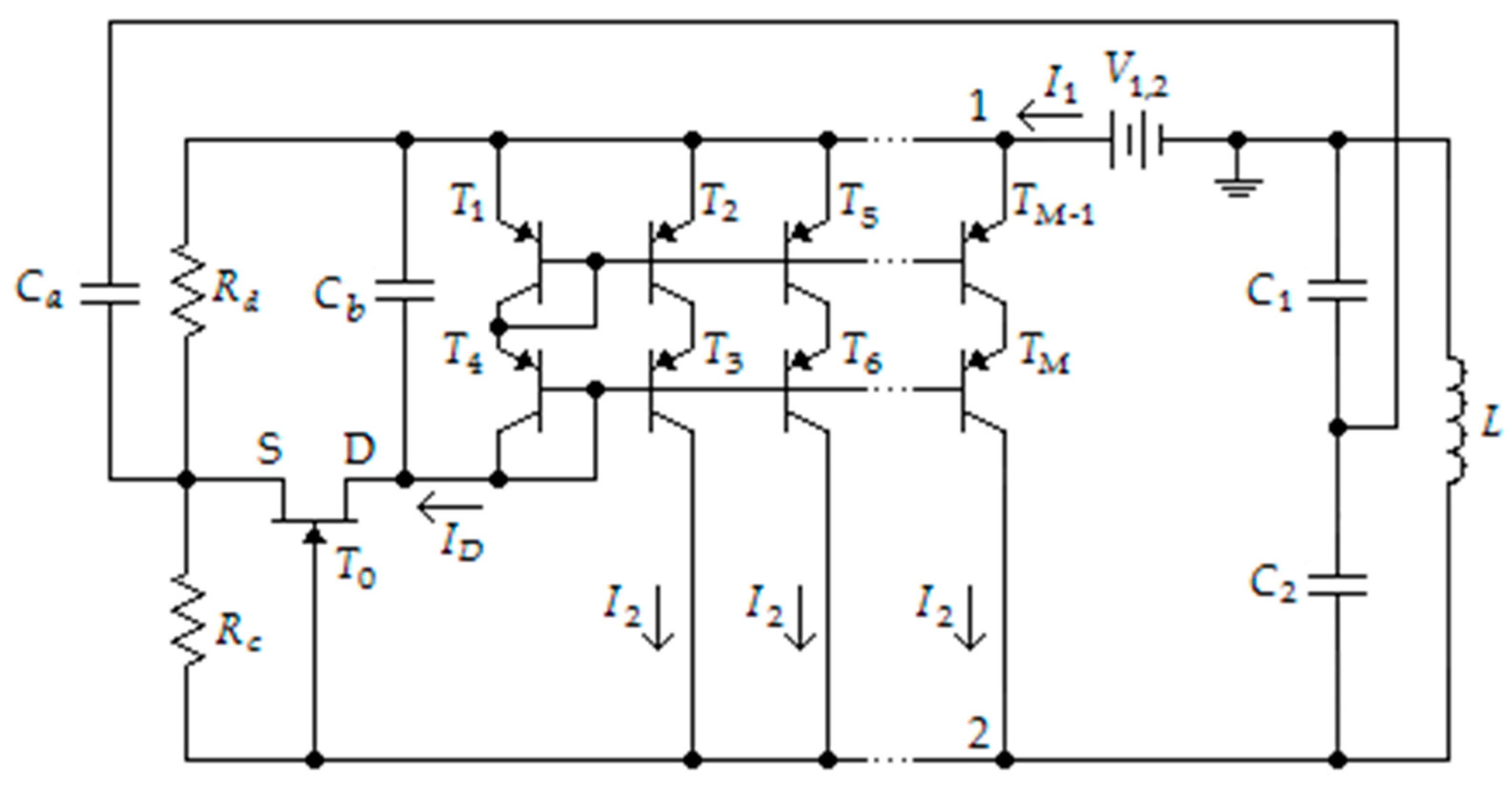
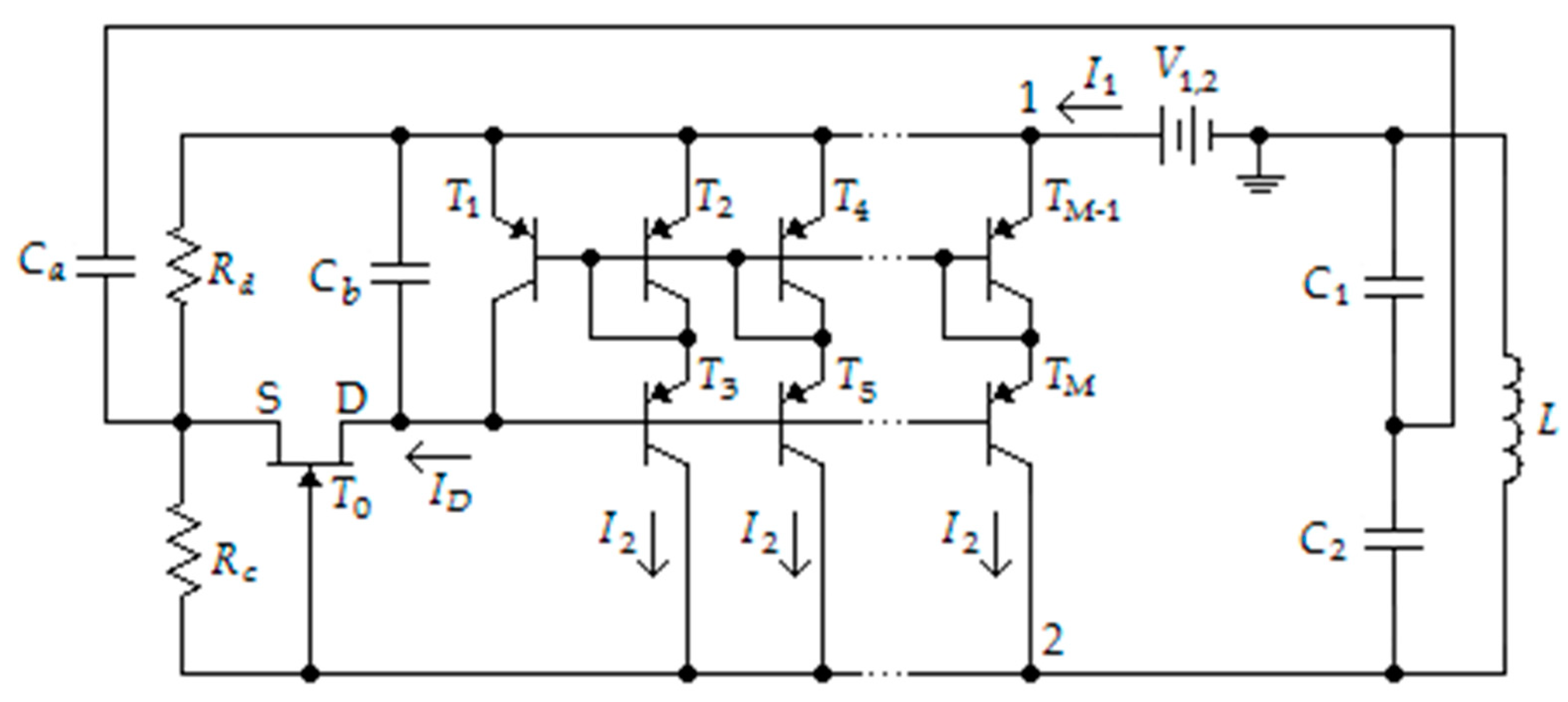
6.1. Negative Differential Resistance Oscillators

The two-terminal circuits shown in Figure 3, Figure 4 and Figure 5 can be used for constructing single-frequency NDR oscillators. Figure 6, Figure 7 and Figure 8 show the NDR oscillators based on MCCM, MWCM, and MIWCM.
In the oscillator circuits of Figure 6, Figure 7 and Figure 8, capacitors C1, C2, and inductor L establish a resonant tank circuit. Capacitor Ca is a feedback element used to improve the start-up of the oscillator. Capacitor Cb serves as a noise killer at the drain of transistor T0.
We show later that the NDR oscillator performance depends on the selected CM and the number of additional current sources I2.
The main characteristics of oscillators are frequency of operation, phase noise, harmonic distortions, and power consumption. Designers use several merit figures combining some or all of the key features to compare different oscillators [46,47].
The most common figure of merit (FOM) is given by [48]
F O M ( f o f ) = P N ( f o f ) d B c 20 log ( f c / f o f ) + 10 log ( P d i s / 1 mW ) ,
where fof is the offset frequency from the carrier frequency fc, PN(fof) is the oscillator phase noise at offset frequency fof, and Pdis is the oscillator dissipation power. The second term allows us to compare oscillators operating at different frequencies. Thus, this criterion is invariant to the oscillator frequency.
According to (22), the less FOM, the more efficient oscillator.
For self-excitation of the oscillator, it is necessary to compensate for the tank circuit’s losses. Negative differential resistance of the oscillator’s electronic circuit carries such compensation for the tank circuit losses. Therefore, the condition for self-excitation of the NDR oscillator has the following form [49]:
| R d i f f | < R Q ,
where |Rdiff| is the absolute value of the NDR at the operating point calculated by (19)–(21), and RQ is the loaded tank circuit resistance at the resonance.
The loaded tank circuit resistance at resonance is [50] (p. 905)
R Q = ρ Q l ,
where ρ is the characteristic impedance of the tank circuit, and Ql is the loaded quality factor of the tank circuit.

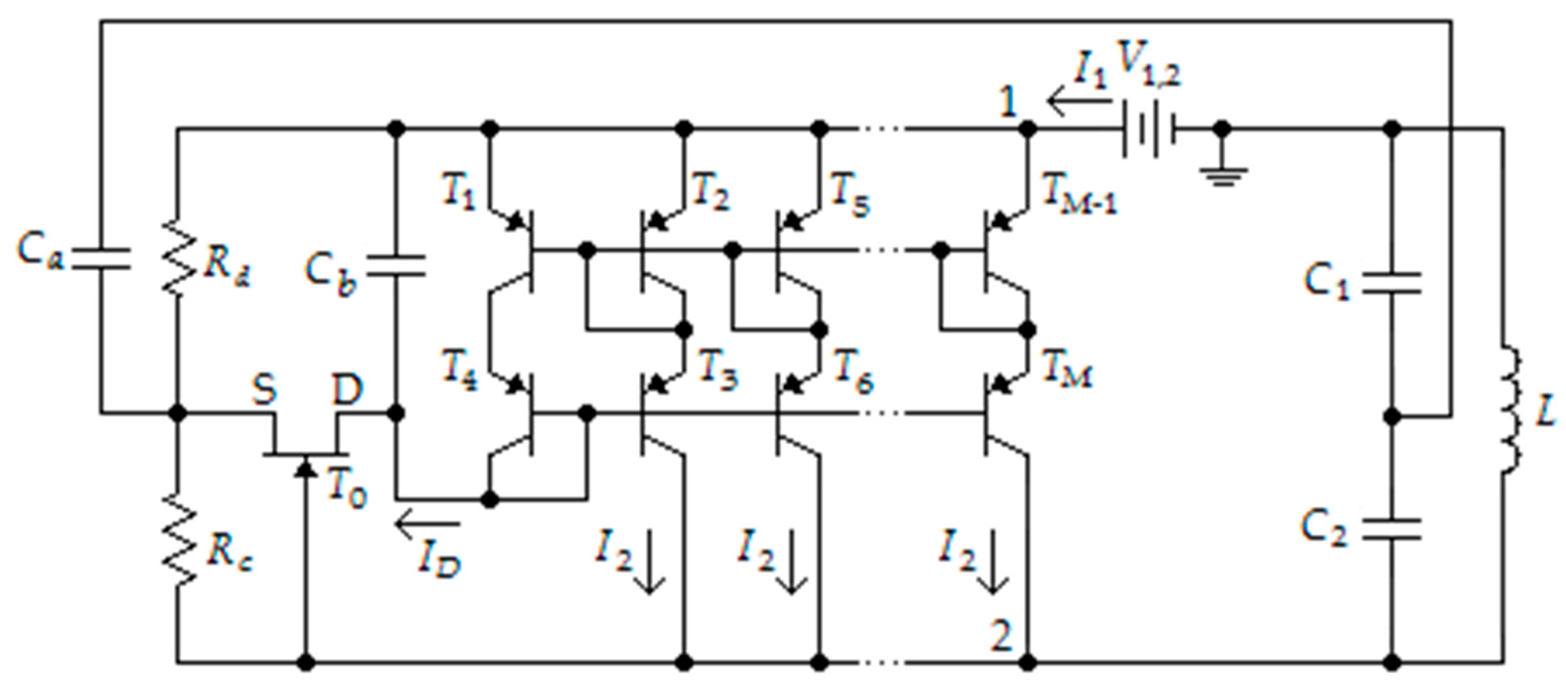
6.2. Negative Differential Resistance Voltage-Controlled Oscillators

Voltage-controlled oscillators are crucial elements of modern instrumentation, communication, navigation, and radar systems. We can classify VCOs as negative impedance (NI) and NDR oscillators. In the NI VCOs, the real part of the input impedance has a negative sign [51,52]. This negative resistance compensates for the losses in the tank circuit. In the NDR VCOs, a negative resistance induced into the tank circuit neutralizes the tank circuit losses; this resistance is inversely proportional to the absolute value of Rdiff [53].
The two-terminal circuits of Figure 3, Figure 4 and Figure 5 can be the base of NDR VCOs. Figure 9, Figure 10 and Figure 11 show the NDR VCOs based on MCCM, MWCM, and MIWCM. In the VCO circuits, instead of capacitors C1 and C2, two oppositely connected varactors, Var1 and Var2, are used. A voltage source Vvar applies dc voltage to the cathodes of varactors. Resistor R0 is linked with the voltage source Vvar, preventing the parallel tank circuit’s shunting.
Further, we use FOM (22) to compare VCO circuits shown in Figure 9, Figure 10 and Figure 11.

7. Results and Discussion

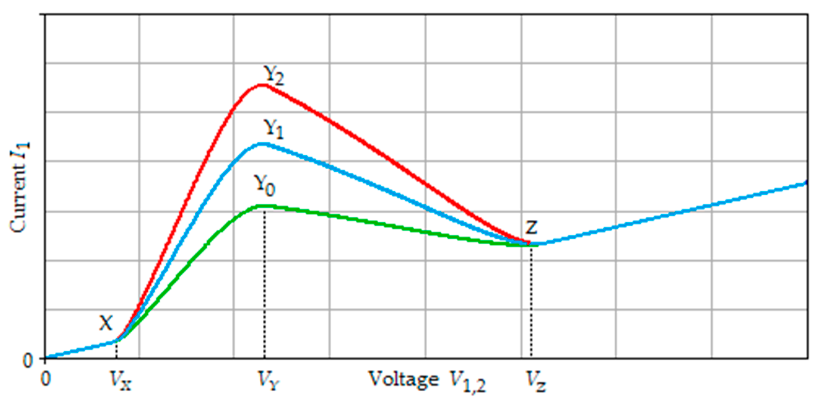
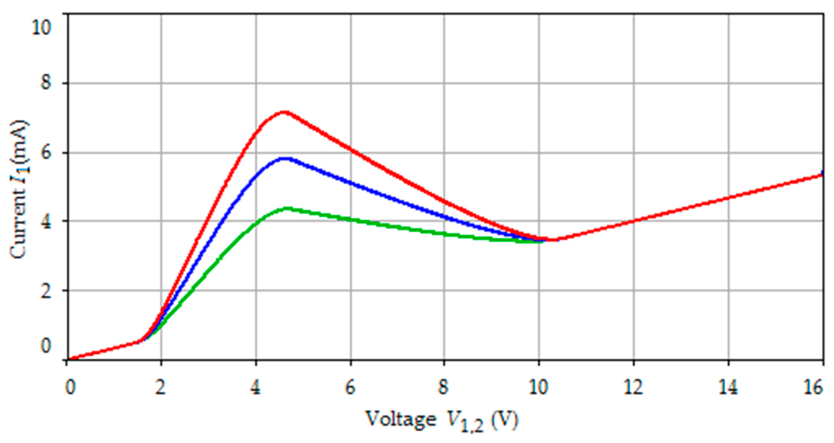
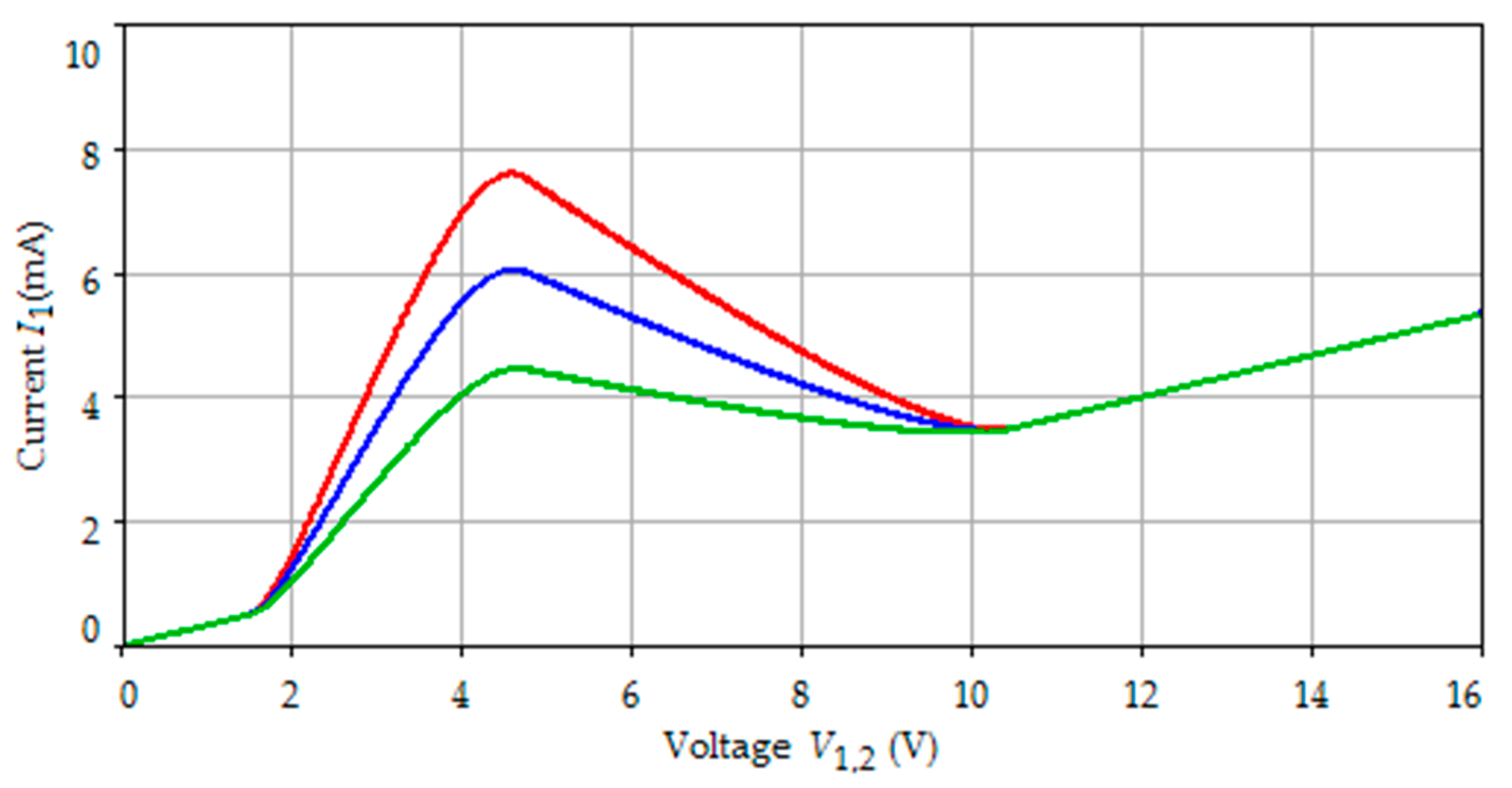
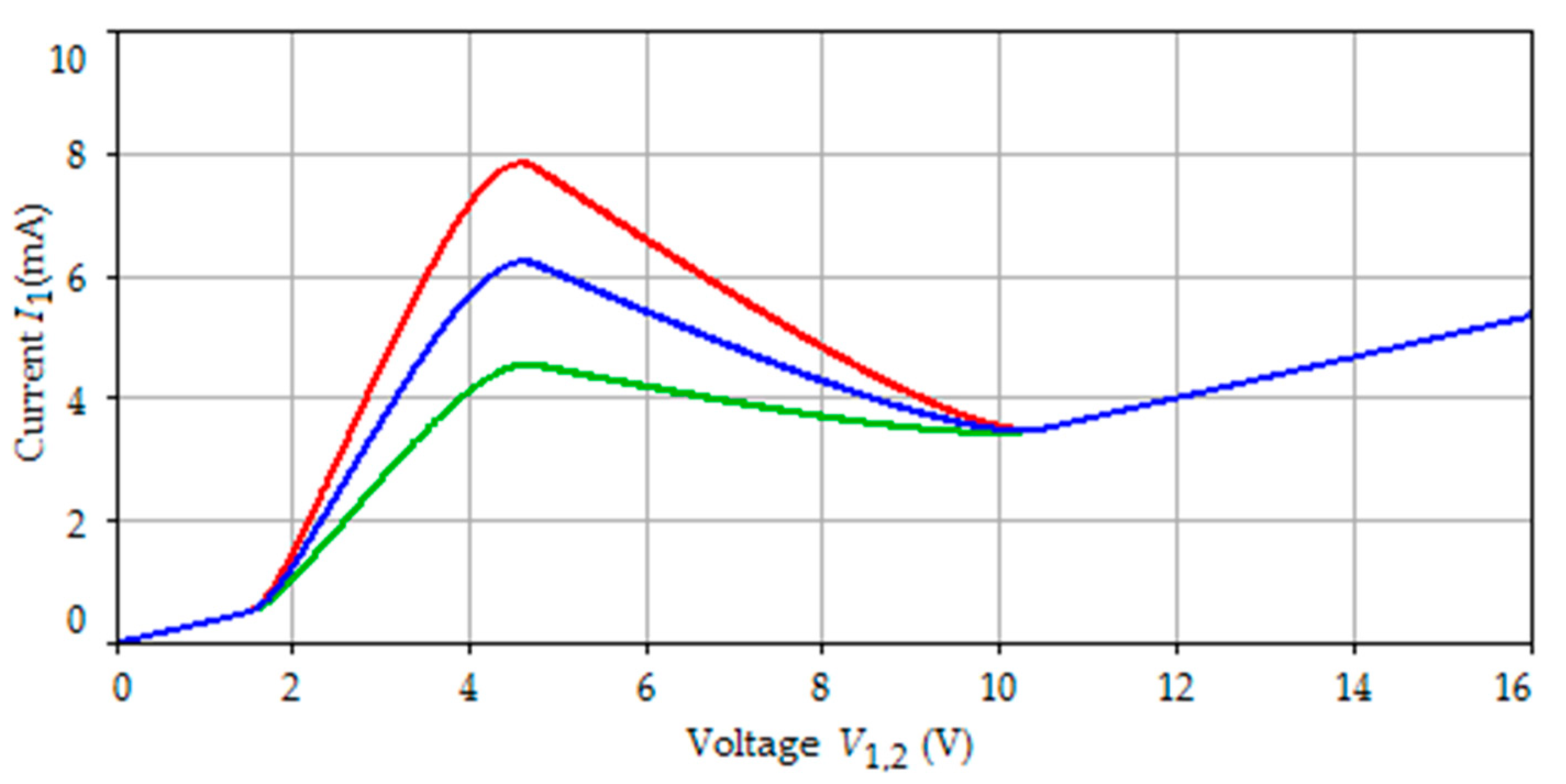
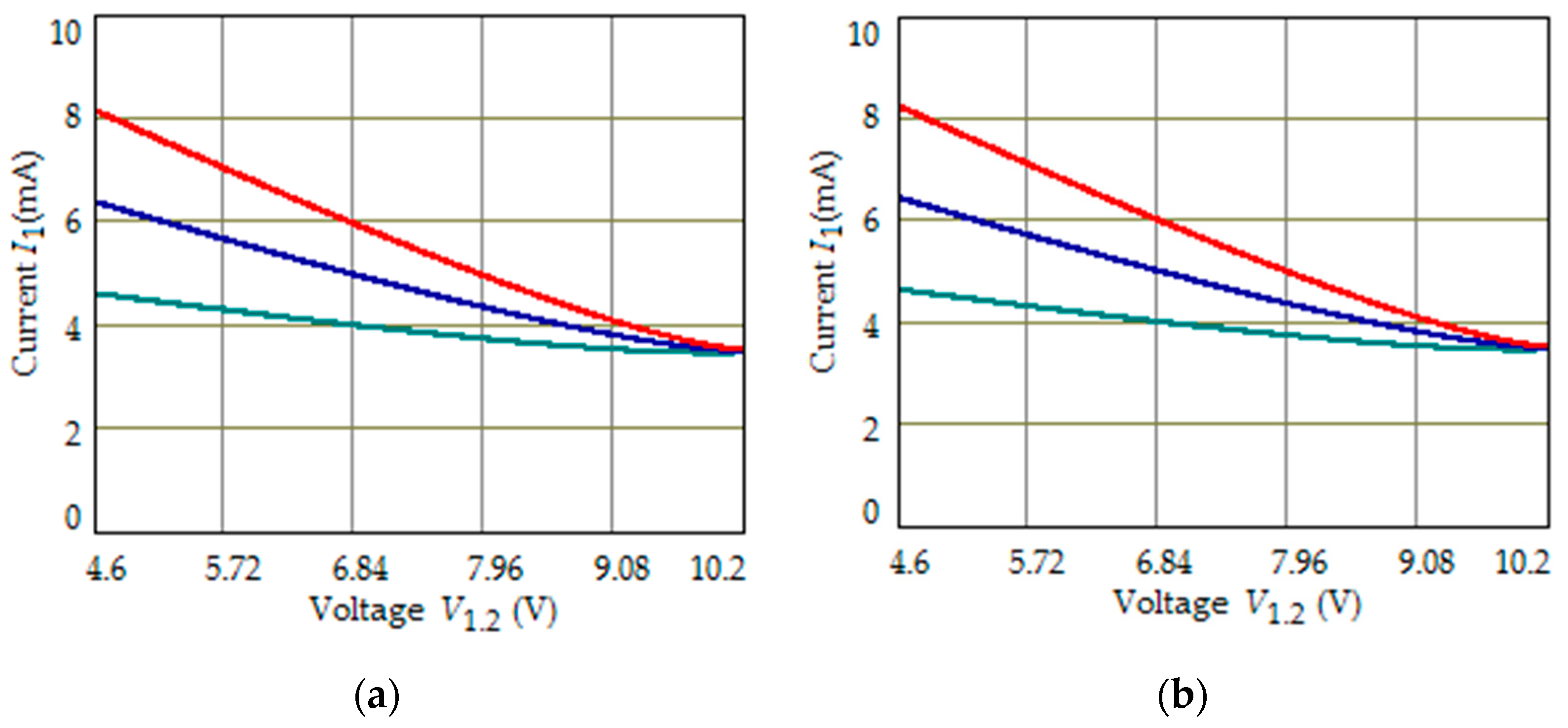
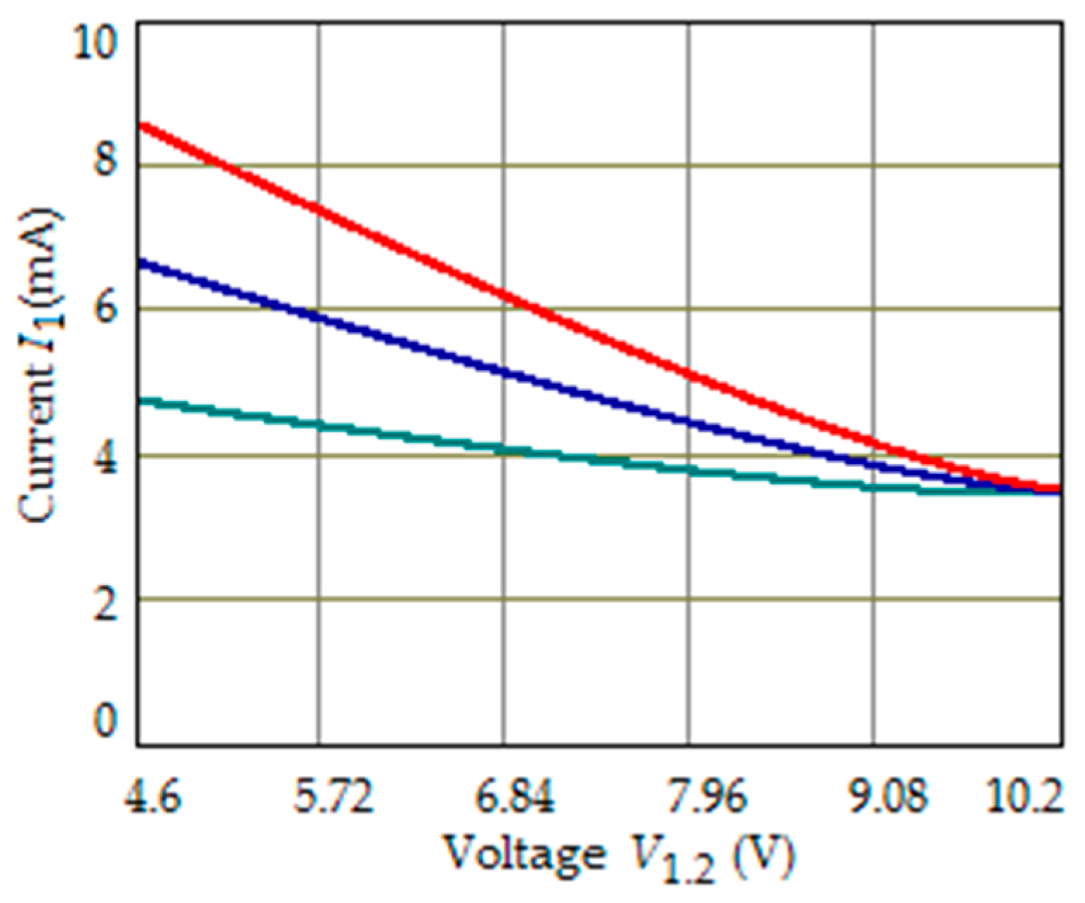
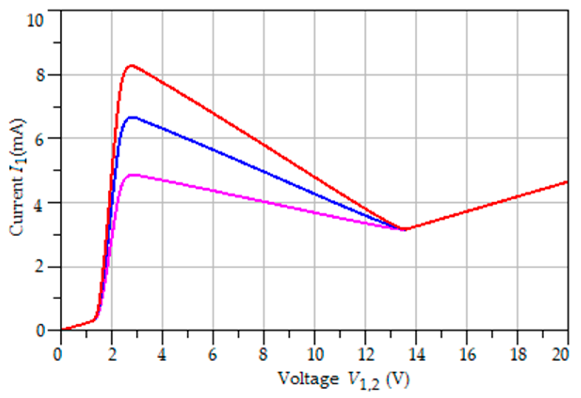
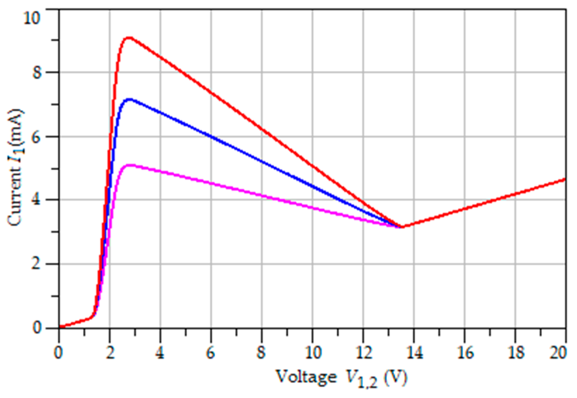
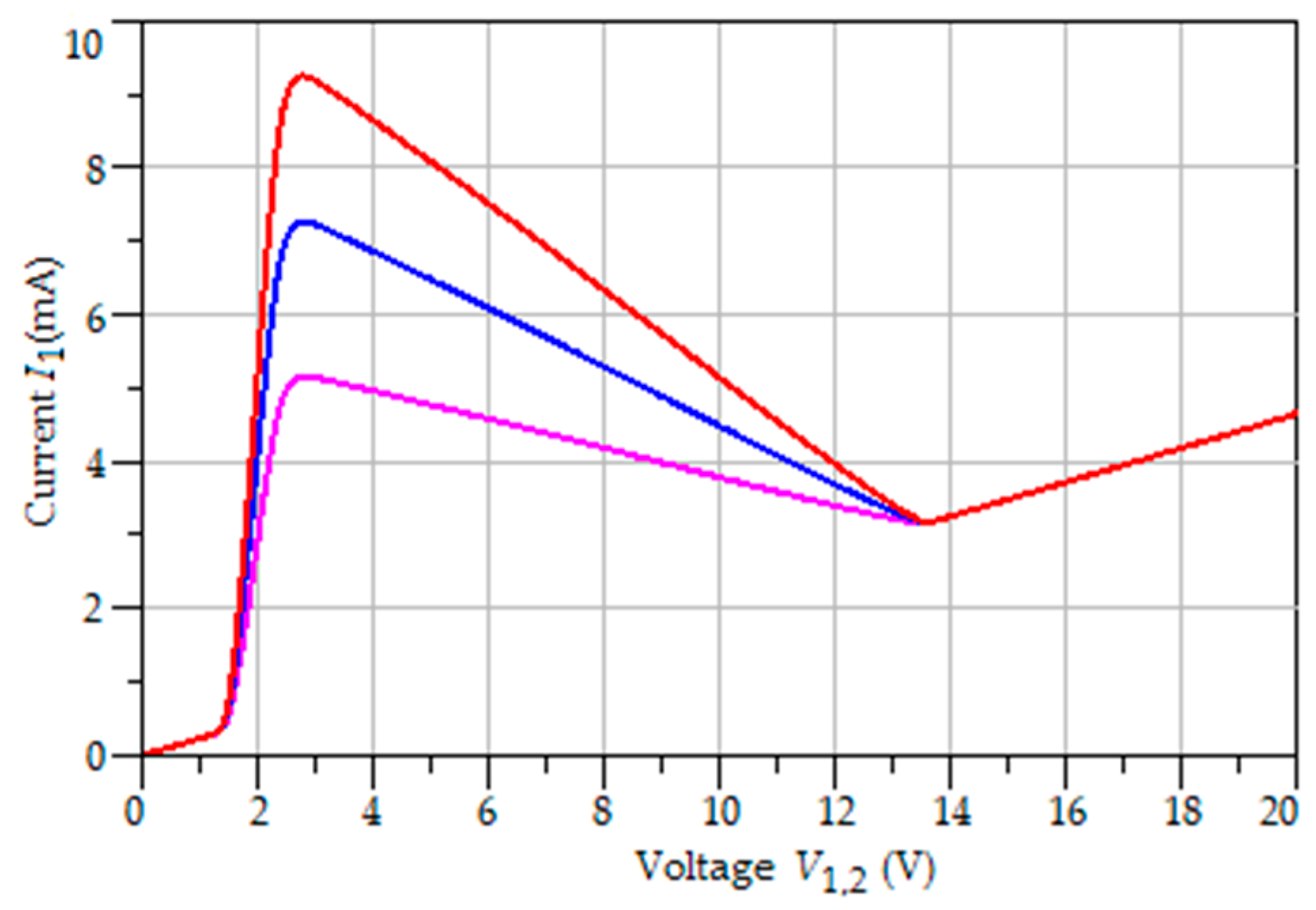
7.1. Simulation and Calculation of Current-Voltage Characteristics

Let us simulate the current-voltage characteristics for two-terminal NDR circuits presented in Figure 3, Figure 4 and Figure 5 by Multisim 14.0. As transistor T0, we use MMBFU310LT1 and BFT92W as transistors in current mirrors. We select the following resistor values: Rc = 1 kΩ and Rd = 2 kΩ.
Figure 12, Figure 13 and Figure 14 show the current-voltage characteristics for the two-terminal NDR circuits with different multiple-output CMs. Table 1 shows the values of voltages and currents at the breakpoints of the curves. Analysis of current-voltage characteristics in Figure 12, Figure 13 and Figure 14 and data in Table 1 leads to the following conclusions: all two-terminal NDR circuits have the same voltages VX, VY, and VZ and currents IX and IZ for any value of m, two-terminal NDR circuit with MCCM has the smallest value of current IY for any value of m, two-terminal NDR circuit with MIWCM has the most considerable value of current IY for any value of m, and two-terminal NDR circuits with MCCM, MWCM, and MIWCM have almost linear dependence of current on voltage in the NDR region.
Since current IZ is the same for all two-terminal NDR circuits, and current IY is different, the slope of the current-voltage characteristics in the NDR region is higher for the greater value of current IY. Therefore, we can order the absolute negative resistance values of various two-terminal NDR circuits according to the following inequality:
| R d i f f C | > | R d i f f W | > | R d i f f I W | ,
where | R d i f f C | ,   | R d i f f W | , and | R d i f f I W | are, respectively, the absolute values of NDR in the two-terminal circuits with cascode, Wilson, and improved Wilson CM.
Thus, inequalities (23) and (25) indicate that the oscillator with multiple-output improved Wilson CM has the most considerable self-excitation ability. In addition, the oscillator with multiple-output cascode CM has the least self-excitation ability.
For comparison with the simulation results, we calculate the current I1 using (3), (5), and (7) with the following data of transistors MMBFU310LT1 and BFT92W: IDSS = 50 mA, VP = –3.5 V, VA = 11 V, and VEB3 = 0.6 V. We use the same values of resistors Rc and Rd as in the simulation.
Figure 15 and Figure 16 show the calculated dependences of current-voltage characteristics in the NDR region for different two-terminal circuits. Table 2 and Table 3 show the calculated currents IY and IZ and the relative accuracy of the IY current calculation ΔIY %, where ΔIY % is given by
δ I Y % = I Y ( calculated ) I Y ( simulated ) I Y ( calculated ) × 100 % .
As shown in Table 3, the highest accuracy of current IY calculation when m = 0 belongs to Equations (5) and (7) for the two-terminal NDR circuit with an MWCM and MIWCM. The highest accuracy of the current IY calculation when m = 1, 2 has Equation (5) for the two-terminal NDR circuit with an MWCM. The worst accuracy of the current IY calculation when m = 0, 1, 2 has Equation (3) for the two-terminal NDR circuit with an MCCM.
In general, we should note that the worst accuracy does not exceed 12.3%, which indicates a sufficient engineering accuracy for calculating the current IY. A practically zero error exists in calculating the current IZ.
Now, let us simulate the current-voltage characteristics for two-terminal NDR circuits presented in Figure 3, Figure 4 and Figure 5 when transistor T0 is a PHEMT. We select ATF34143 as transistor T0 and MRFC521 as transistors in BJT CM and choose the following resistor values: Rc = 300 Ω and Rd = 4 kΩ.
Figure 17, Figure 18 and Figure 19 show the current-voltage characteristics for the PHEMT based two-terminal NDR circuits with different multiple-output CM. Table 4 shows the values of voltages and currents at the breakpoints of characteristics. From the analysis of Table 4, the same conclusions follow as from the study of Table 1. As in using JFET, the PHEMT based two-terminal circuits also have a linear current dependence on voltage in the NDR region.
We also calculate the current I1 at voltages VX, VY, and VZ using Equations (3), (5) and (7) with the following data of transistors ATF34143 [54] and MRFC521: b = 0.24 A/V2, VTH = –0.95 V, α = 4 V−1, λ = 0.09 V−1, hFE = 50, VA = 15 V, VEB3 = 0.7 V. The values of resistors Rc and Rd are similar to those used in simulation.
Table 5 and Table 6 show the calculated currents IY and IZ and the relative accuracy of the IY current calculation ΔIY %. The conclusions concerning the accuracy of the current IY calculation for Table 6 are the same as those for Table 3.
We should note that the accuracy of calculating the current ID by Formula (17) is quite high. Indeed, for all two-terminal NDR circuits at VY = 2.8 V, the current ID(simulated) = 2.79 mA, and the current ID(calculated) = 2.67 mA. Therefore, ΔID % = –4.5 %, where ΔID % is the relative accuracy of calculating the current ID by formula
δ I D % = I D ( calculated ) I D ( simulated ) I D ( calculated ) × 100 % .

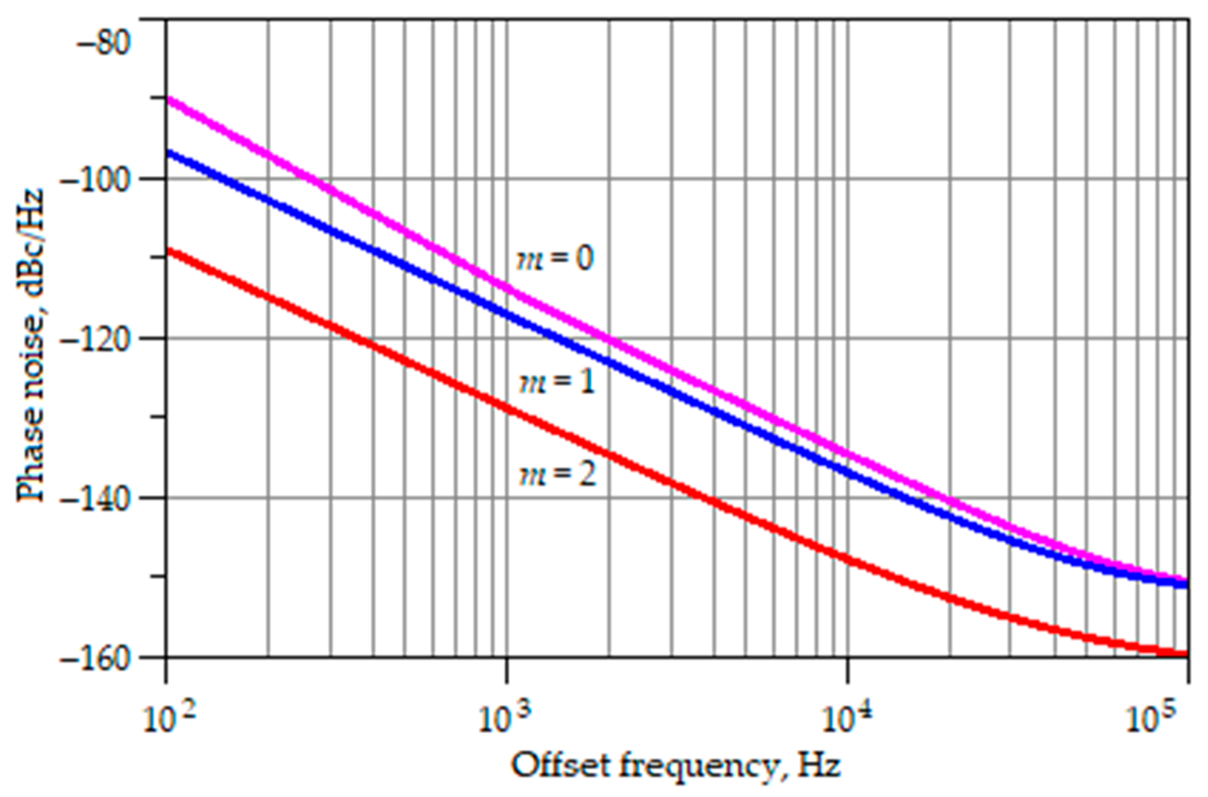
7.2. Simulation of Negative Differential Resistance

By inequality (23), the steepness of the current-voltage characteristics in the vicinity of the operating point significantly affects the self-excitation of an oscillator. The less the absolute value of the differential resistance, the greater is the probability of self-excitation of the oscillator.
Table 7 shows the simulation results of the differential resistance at the operating point V1,2 = 4 V for two-terminal NDR circuits shown in Figure 3, Figure 4 and Figure 5 using the same input data as Table 4. As shown in Table 7, the smallest absolute value of NDR at the operating point has a two-terminal NDR circuit with an improved Wilson CM. The NDR circuit with a Wilson CM has a little greater absolute value of NDR. The circuit with a cascode CM has the most considerable absolute value of NDR for any m. Thus, the improved Wilson and Wilson CM oscillators have the best start-up conditions due to inequality (23).

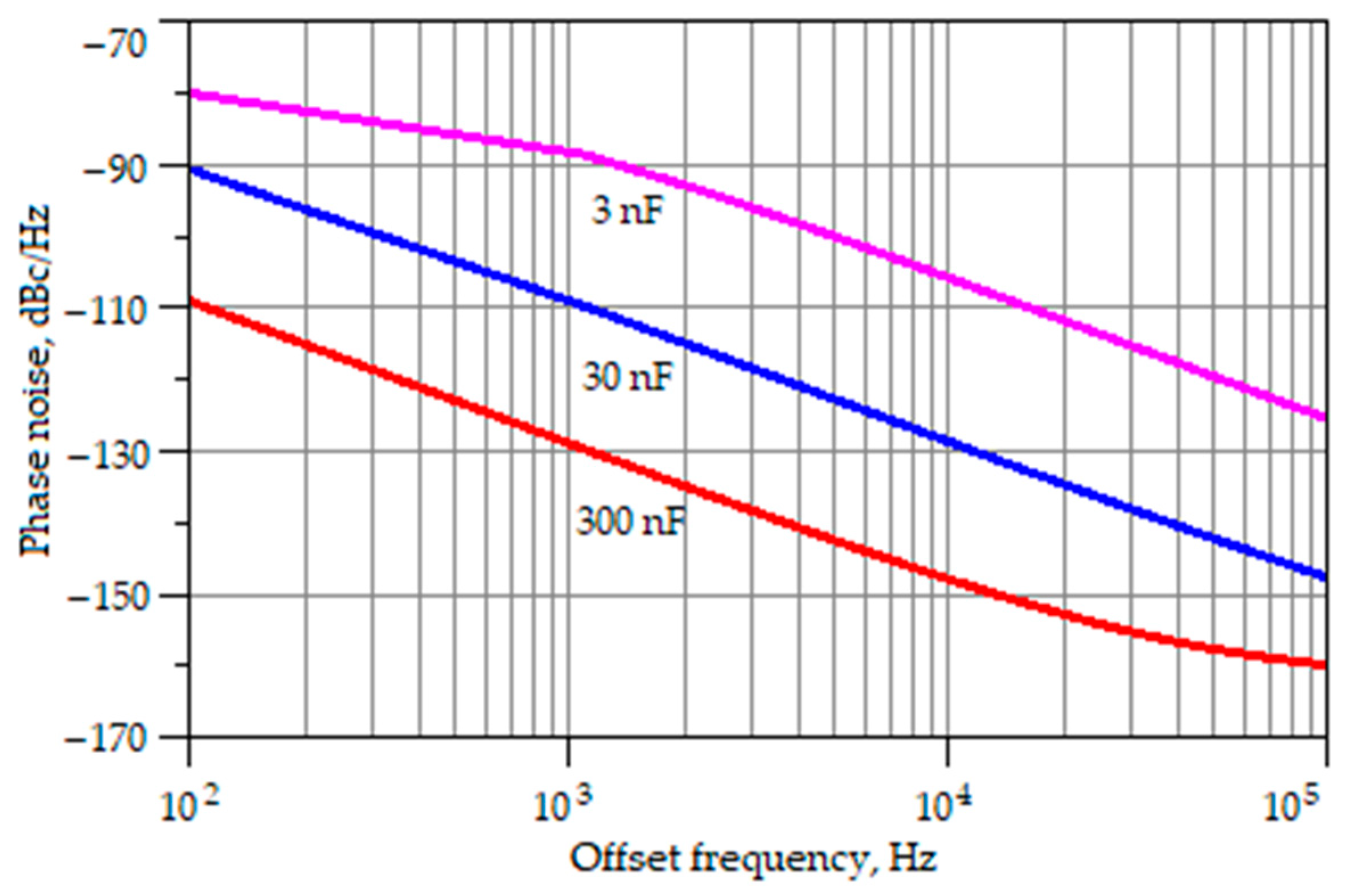
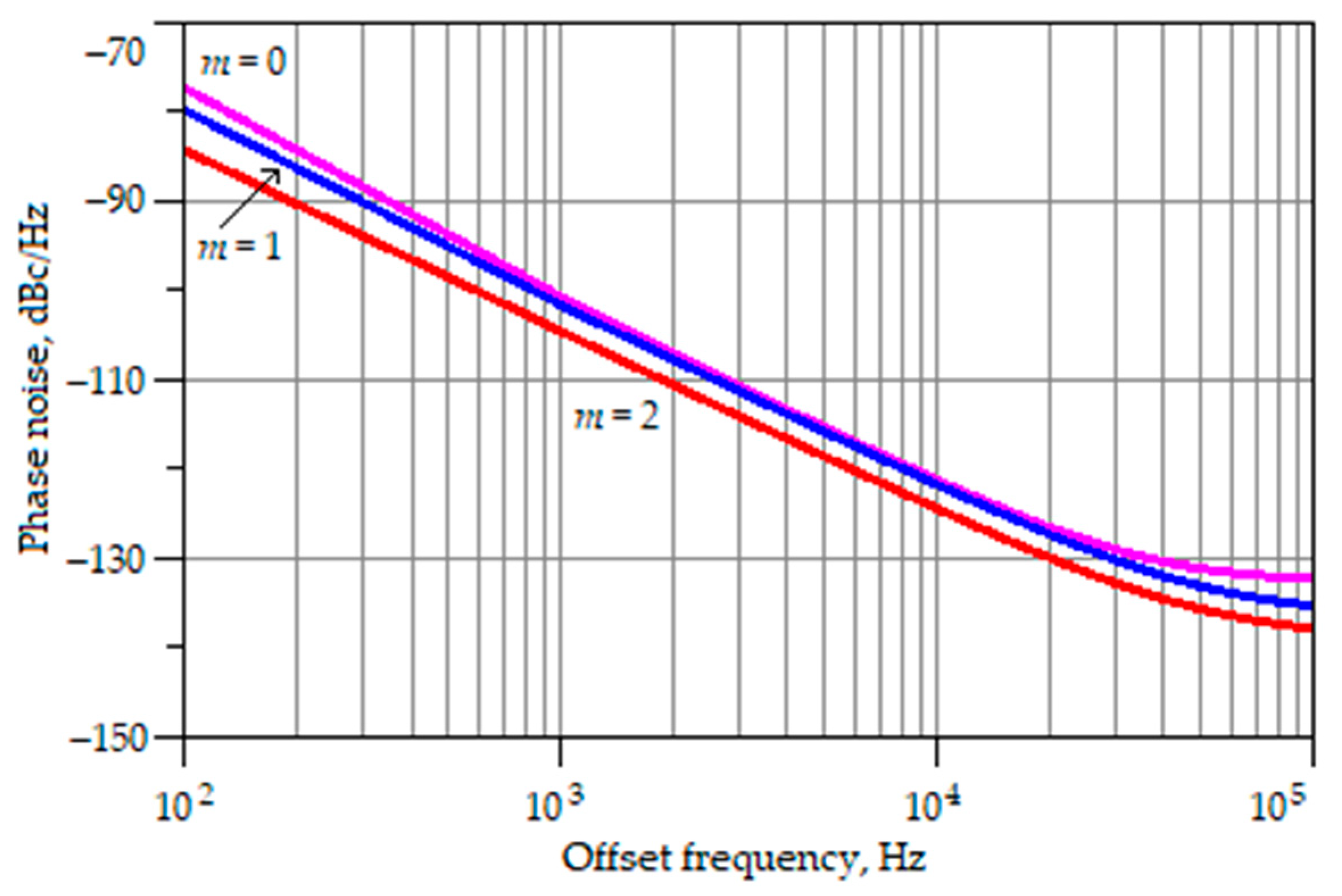
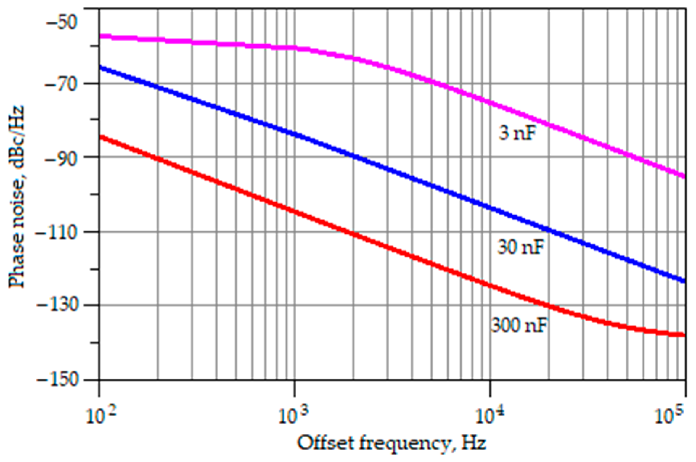
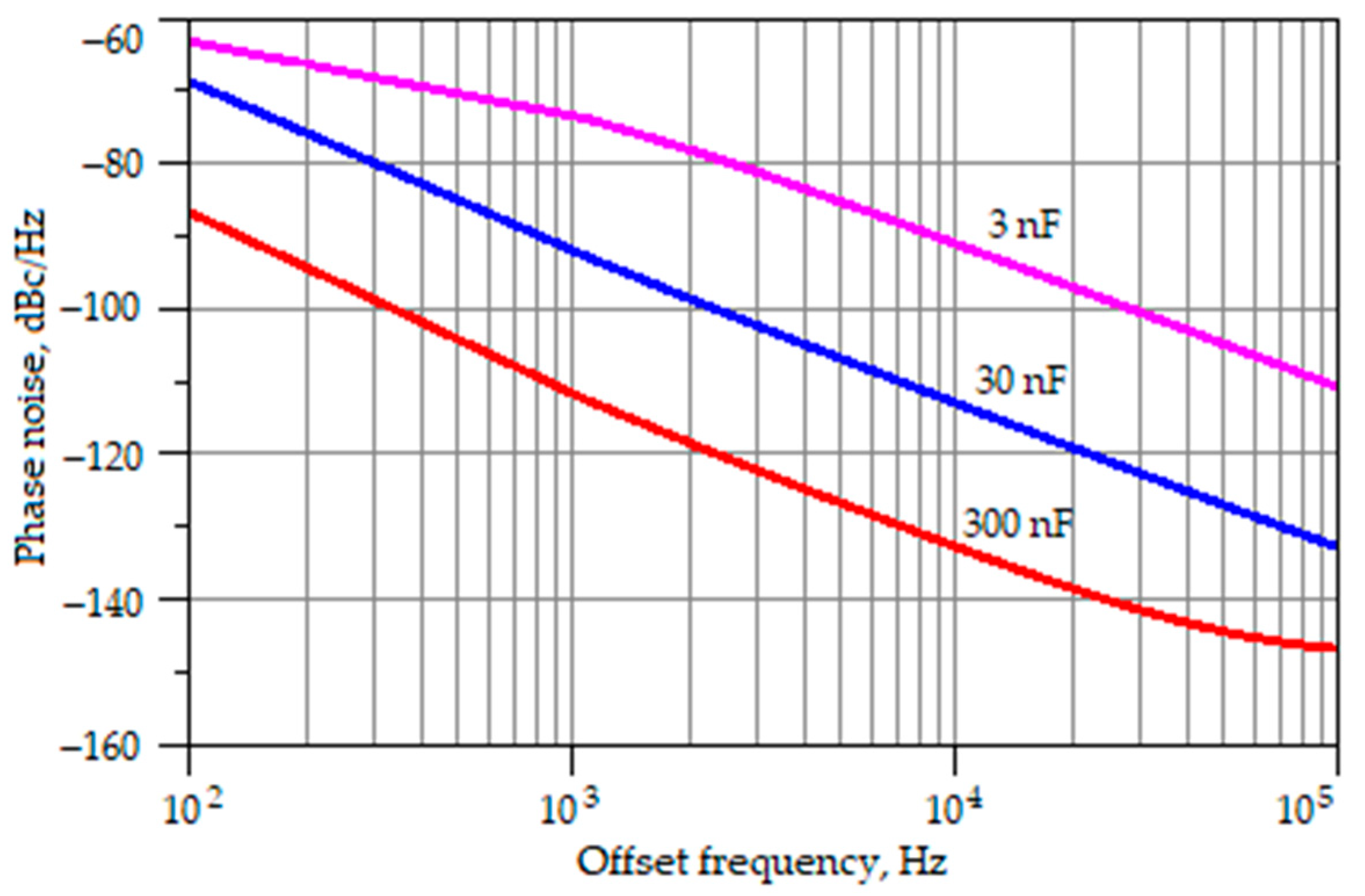
7.3. Simulation of Oscillator Characteristics

Let us simulate the characteristics for oscillators presented in Figure 6, Figure 7 and Figure 8 by ADS2020. As transistor T0, we use ATF34143 and MRFC521 as transistors in BJT CM. We select chip inductor 0604HQ-1N1XJR (1.15 nH), and C1 = C2 = 1 pF, Rc = 300 Ω, Rd = 4 kΩ, Cb = 300 nF, and V1,2 = 4 V for all oscillators. We selected the value of capacitance Ca from the condition of minimizing the phase noise of each oscillator.
We use FOM (22) to compare oscillators shown in Figure 6, Figure 7 and Figure 8. Table 8 shows the results of the oscillators’ simulation under the assumption that load resistance (RL) is infinite.
As shown in Table 8, oscillators with MCCM, MWCM, and MIWCM have the best FOM value when m is 0, 2, and 1, respectively. Among all oscillators, the best FOM of −227.1 dBc/Hz has the one with MWCM when m = 2. For each value of m in Table 8, oscillators with MWCM and MIWCM have significantly better FOM than the oscillator with MCCM. For each value of m, the oscillator with MCCM has the highest oscillation frequency, the lowest power of dissipation, and the worst phase noise.
Figure 20 shows the dependence of phase noise versus offset frequency for the oscillator with MWCM. As shown in Figure 20, the best value of phase noise of −159.9 dBc/Hz at an offset frequency of 100 kHz is the case when m = 2 and Ca = 3 pF.
Figure 21 shows the dependence of phase noise versus capacitance Cb for the oscillator with multiple-output Wilson CM. We can see from Figure 21 that oscillator phase noise significantly depends on the value of Cb. Indeed, when capacitance Cb varies from 3 to 300 nF, phase noise decreases from −125.5 to −159.9 dBc/Hz. We can explain such a decrease in phase noise by reducing noise spectral density at the drain of transistor T0 where capacitor Cb is connected.
Let us now consider the case when a load RL is connected through the capacitive divider to an oscillator output, as shown in Figure 22. Assume that RL = 50 Ω and CCD1 = CCD2 = 0.5 pF for the oscillators with MIWCM (m = 0, 1, 2) and MWCM (m = 0). For the oscillators with MCCM (m = 0, 1, 2) and MWCM (m = 1, 2), we selected CCD1 = CCD2 = 0.25 pF.
Using FOM (22), we compare oscillators shown in Figure 6, Figure 7 and Figure 8 when RL = 50 Ω. Table 9 shows the results of the oscillators’ simulation. As shown in Table 9, the best FOM values correspond to the same m sequence (0, 2, 1) as when RL = ∞ for oscillators with MCCM, MWCM, and MIWCM.
Table 10 shows the performance comparison of oscillators with MCCM, MWCM, and MIWCM for RL = ∞ and RL = 50 Ω.
As we can see in Table 10, the performance of each oscillator reduces when a 50 Ω load is connected to its output. The oscillator’s performance with MICCM decreases to the greatest extent, and the oscillator’s performance with MIWCM drops to the least. The absolute FOM value decreases by 4.9% and 0.8% in relative units, respectively, i.e., not critical.

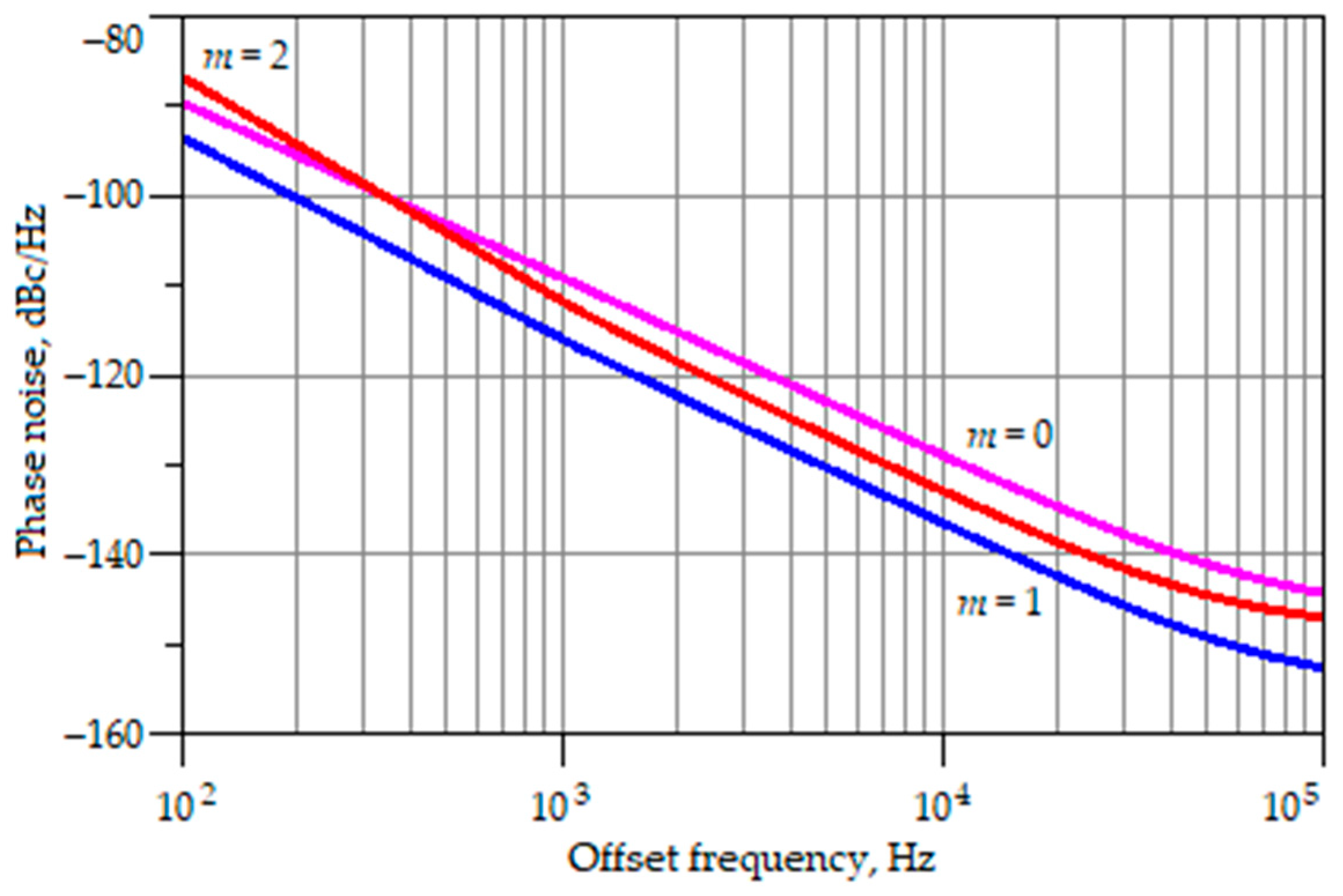
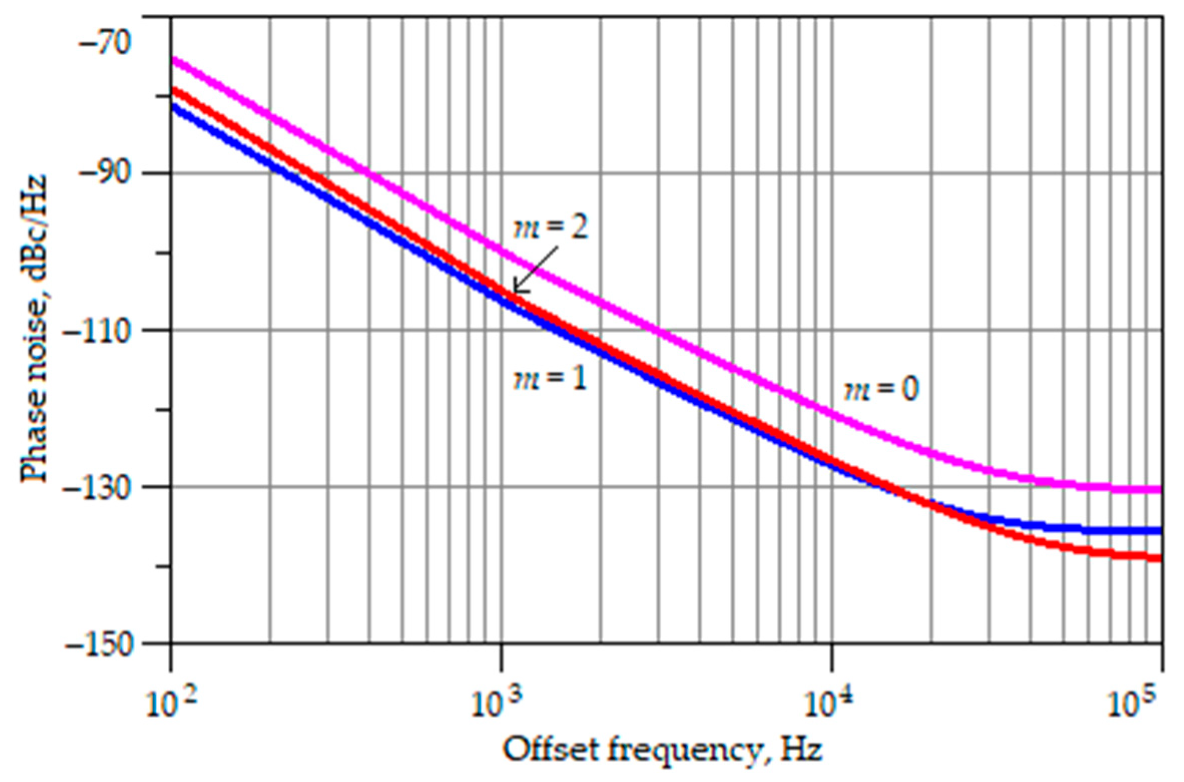
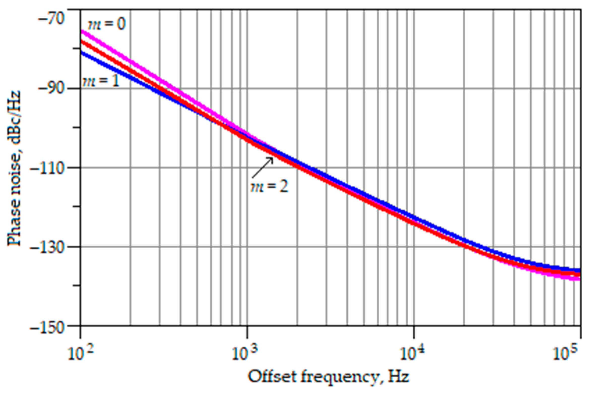
7.4. Simulation of VCO Characteristics

Let us now simulate the characteristics for VCOs presented in Figure 9, Figure 10 and Figure 11 by using the same transistors, resistor values of Rc and Rd, inductor type of L, and power supply voltage as in Section 7.3 when RL = ∞. We select varactors SMV1104-33. The tuning voltage Vd is varied from 2 to 12 V for each VCO. Capacitance Cb = 50 nF for VCOs with MCCM and Cb = 300 nF for VCOs with MWCM and MIWCM.
As in Section 7.3, we select the value of capacitance Ca from the condition of minimizing the phase noise of each VCO.
Figure 23 and Figure 24 show the dependence of phase noise versus offset frequency for VCOs with MIWCM at Vd = 2 V and Vd = 12 V. The best value of phase noise of −137.9 dBc/Hz at an offset frequency of 100 kHz and Vd = 2 V has VCO with MIWCM when m = 2 (see Figure 23). The best value of phase noise of −152.5 dBc/Hz at an offset frequency of 100 kHz and Vd = 12 V also has VCO with MIWCM but when m = 1 (see Figure 24).
Interestingly, at Vd = 2 V, the phase noise improvement occurs in the sequence of m = 0, 1, 2, i.e., the more mirrored currents, the lower the phase noise (see Figure 23). However, at Vd = 12 V, the phase noise improvement occurs in m = 0, 2, 1, i.e., the highest phase noise occurs at m = 0, and the lowest at m = 1 (see Figure 24). The phase noise curve at m = 2 occupies an intermediate position.
Table 11 shows the simulated characteristics of different VCOs when RL = ∞, where fmin and fmax are the minimum and maximum frequency of VCO operation. As shown in Table 11, the VCO with MCCM has the best performance when m = 0. The VCO with MWCM achieves the best performance when m = 2 and VCO with MIWCM—when m = 1. For each value of m in Table 11, VCO with MWCM and MIWCM have significantly lower (i.e., better) FOM than VCO with MCCM. The broadest tuning frequency range, Δf = 370 MHz, has VCO with MCCM when m = 0. The lowest power consumption, Pdis = 18.8 mW, also has VCO with MCCM when m = 0.
Figure 25 and Figure 26 illustrate the dependence of phase noise versus capacitance Cb for VCO with multiple-output improved Wilson CM at Vd = 2 V and Vd = 12 V, respectively. We can see from Figure 25 and Figure 26 that VCO phase noise significantly depends on the value of capacitor Cb. Indeed, when capacitance Cb varies from 3 to 300 nF, phase noise decreases from −95.3 to −137.9 dBc/Hz at Vd = 2 V and from −110.9 to −146.9 dBc/Hz at Vd = 12 V. We can explain such a decrease in phase noise by reducing noise spectral density at the drain of transistor T0.
Table 12 shows the simulated characteristics of different VCOs when a 50 Ω load through a capacitive divider (see Figure 22) is connected to the output of VCOs shown in Figure 9, Figure 10 and Figure 11.
We select CCD1 = CCD2 = 0.5 pF for the VCOs with MWCM (m = 0, 1, 2), and MIWCM (m = 1, 2), and CCD1 = CCD2 = 0.25 pF for the VCOs with MCCM (m = 0, 1, 2) and MIWCM (m = 0).
As shown in Table 12, the VCO with MCCM has the best performance when m = 0 and Ca = 30 pF. The VCO with MWCM achieves the best performance when m = 1 and Ca = 20 pF, and the VCO with MIWCM—when m = 2 and Ca = 9 pF.
As in the case of RL = ∞ (see Table 11), for each value of m in Table 12, VCOs with MWCM and MIWCM have significantly lower FOM than VCO with MCCM.
Figure 27 and Figure 28 show the dependence of phase noise versus offset frequency for VCOs with MIWCM at Vd = 2 V and Vd = 12 V when RL = 50 Ω. The best value of phase noise of −139.0 dBc/Hz at an offset frequency of 100 kHz and Vd = 2 V has VCO when m = 2 (see Figure 27).
The best value of phase noise of −138.4 dBc/Hz at an offset frequency of 100 kHz and Vd = 12 V corresponds to m = 0 (see Figure 28).
Table 13 compares the performance of VCOs with MCCM, MWCM, and MIWCM for RL = ∞ and RL = 50 Ω.
As shown in Table 13, the highest (i.e., the worst) in-band value of the FOM insignificantly increases when connecting a 50 Ω load to the VCO output. Indeed, the absolute FOM value decreases by 0.5 dBc/Hz for VCO with MICCM, by 1.6 dBc/Hz for VCO with MWCM, and by 1.1 dBc/Hz for VCO with MIWCM. However, the lowest (i.e., the best) in-band FOM value changes more substantially, namely by 41.1 dBc/Hz for VCO with MCCM, by 4.3 dBc/Hz for VCO with MWCM, and by 16.9 dBc/Hz for VCO with MIWCM. Since, when comparing the VCOs, the worst in-band FOM value is considered, we can conclude that this value changes insignificantly (maximum 0.7 %) when connecting a 50 Ω load to the VCO output.
Table 12 and Table 13 show that the best VCO when RL = 50 is the VCO with MIWCM (m = 2).
Table 14 compares the performance characteristics of the recently published and developed in this article VCOs and oscillators. We can draw the following conclusions from Table 14. The oscillator with MWCM (m = 2, RL = 50 Ω) designed in this study has the lowest phase noise (−154.6 dBc/Hz at 0.1 MHz offset) and the best FOM (−221.6 dBc/Hz) among all oscillators. The latter is an indisputable advantage of the developed oscillator since CMOS oscillators have a much lower power consumption and usually have a significant advantage over GaN and GaAs oscillators in terms of the FOM value.
The designed VCO with MIWCM (m = 2, RL = 50 Ω) also has very low phase noise (−139.0, −137.0 dBc/Hz at 0.1 MHz offset) and is one of the best FOM (−205.1, −203.9 dBc/Hz at 0.1 MHz offset) in the tuning range. Thus, we can successfully use the proposed two-terminal circuits with NDR for constructing highly efficient microwave oscillators and VCOs.

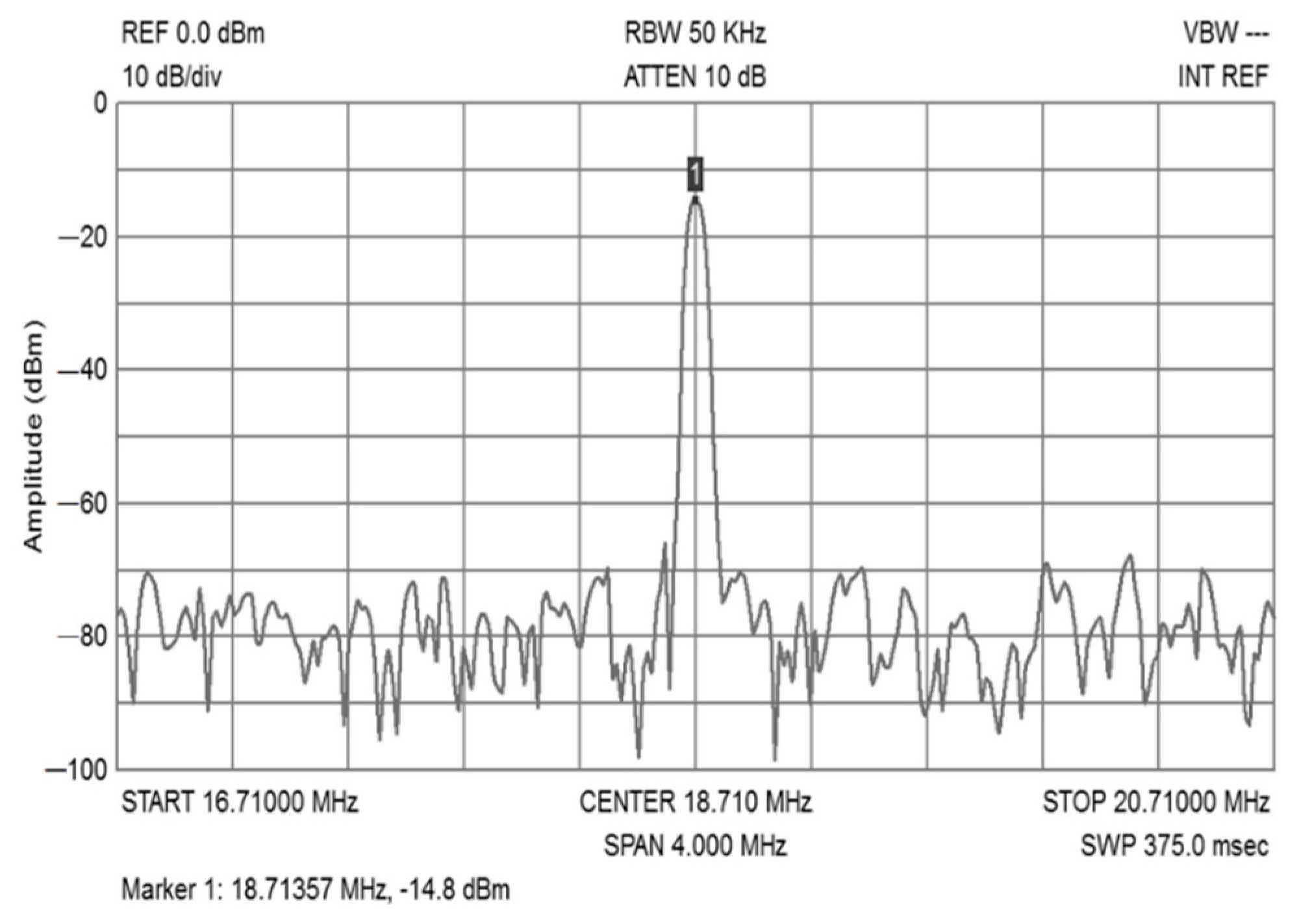
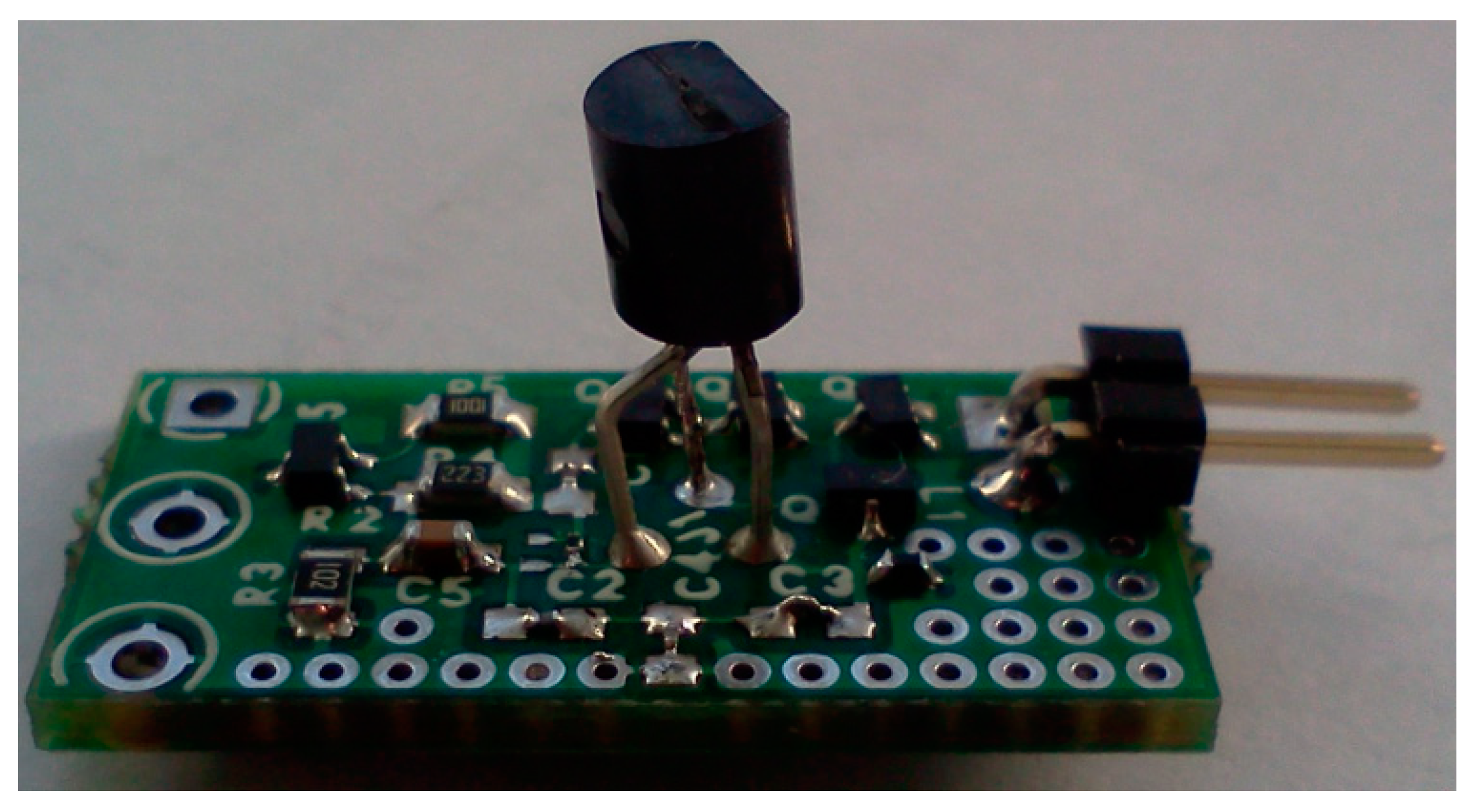
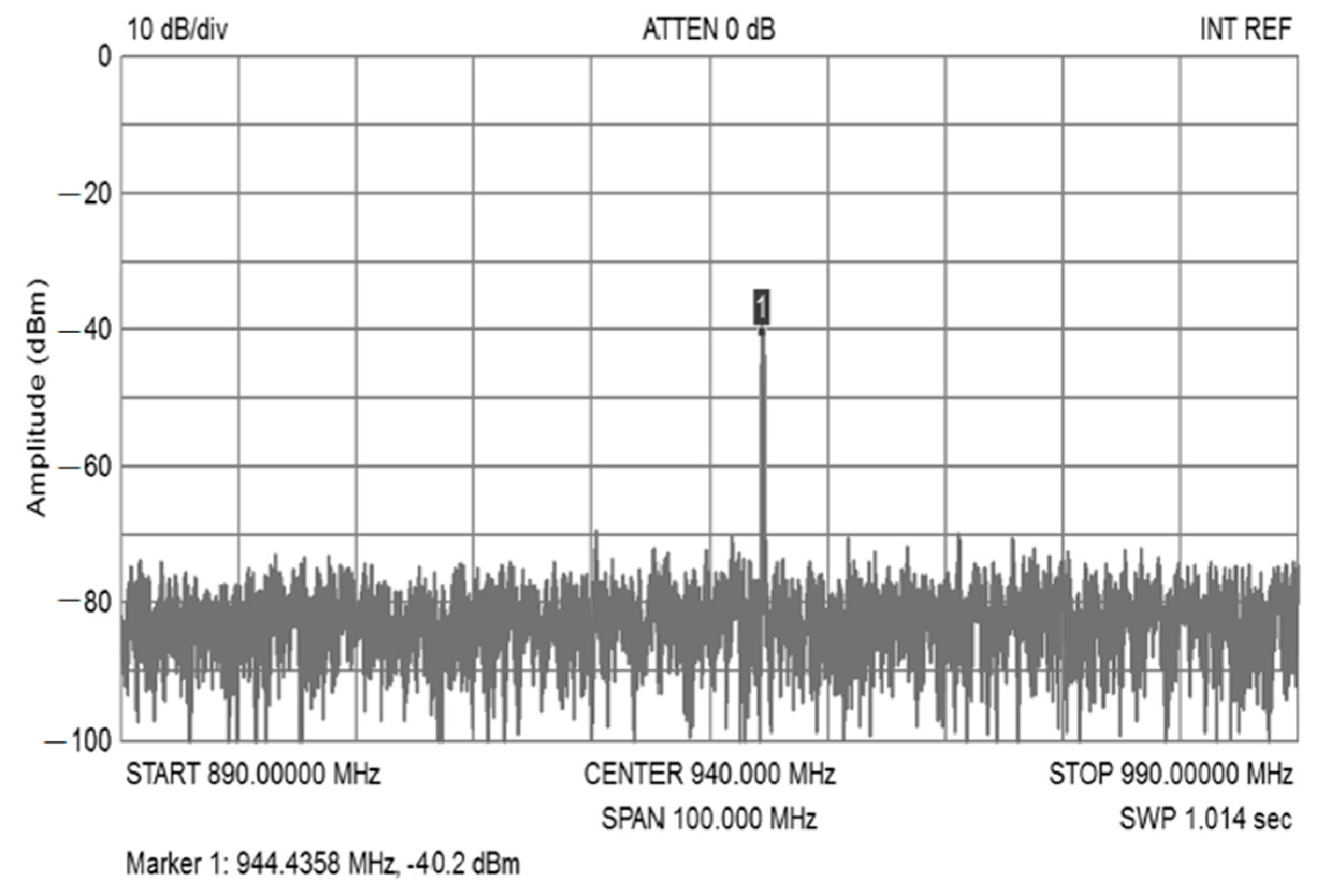
8. Experimental Results

We tested the oscillator circuit with MIWCM (see Figure 8) on a breadboard and printed circuit board (PCB) assembly. Table 15 shows part numbers and nominal values of the breadboard oscillator elements.
In the oscillator circuit with MIWCM of Figure 8, the value of m is equal to 1. At the operating point, V1,2 = 6 V and I1 = 2.7 mA. Figure 29 shows the measured oscillator output spectrum at the fundamental frequency of 18.7 MHz with an output power of −14.8 dBm. We used a spectrum analyzer USB-SA44B (Battle Ground, WA, USA) and an Auburn P-20A RF probe (Auburn, WA, USA) with a 10:1 voltage ratio.
Figure 30 shows the PCB assembly of the oscillator with MIWCM (m =0). Table 16 indicates part numbers and nominal values of components assembled on PCB. We also used the USB-SA44B spectrum analyzer with Auburn P-20A RF probe to measure the oscillator output spectrum (see Figure 31) at V1,2 = 9 V and RBW = 100 kHz. As shown in Figure 31, the oscillation frequency is 944.4 MHz, and the power level of the output signal is −40.2 dBm. In estimating the actual power level, we should consider that the attenuation provided by the P-20A RF probe is 20 dB, and an insertion loss of the buffer amplifier is 2.2 dB.

9. Conclusions

In this article, we have demonstrated new two-terminal NDR circuits based on a combination of a field-effect transistor and multiple-output cascode, Wilson, and improved Wilson BJT current mirrors. The proposed circuits allow controlling the slope of the current-voltage characteristics in the NDR region by changing the number of mirrored currents, thus setting the peak-to-valley current ratio to any desired value. We have conducted modeling total current in the NDR region when the FET is a JFET and MESFET, HEMT, or PHEMT; the obtained current equations calculate the negative resistance at the operating point. We considered possible applications of the proposed two-terminal NDR circuits as oscillators and VCOs. We found that the NDR circuit with multiple-output improved Wilson current mirror has the smallest absolute value of negative resistance, which means that the NDR oscillator based on this circuit has the best conditions for self-excitation. We analyzed the effect of loading on the performance characteristics of the oscillators and VCOs. We found that a 50-ohm load reduces, in comparison to infinite load, the performance of the oscillators and VCOs by a maximum of 4.9% and 0.7 %, respectively. By simulation, we show that the microwave oscillator based on multiple-output improved Wilson current mirror has the lowest phase noise (−154.6 dBc/Hz at offset 100 kHz) and the best figure of merit (−221.6 dBc/Hz) compared to other considered oscillators. We also show that the VCO with multiple-output improved Wilson current mirror has the best FOM in the tuning range (−205.1, −203.9 dBc/Hz). Comparison of the developed oscillators and those previously published showed that the oscillators based on the proposed two-terminal NDR circuits are superior to the well-known GaN and GaAs HEMT oscillators by 10–20 dB with respect to the commonly used figure of merit. It is also interesting to note that the proposed oscillator circuits are higher in effectiveness than even CMOS oscillators, despite the much lower power consumption of the latter. This advantage is due to the low level of phase noise in the designed oscillators.
Our future work will focus on developing and studying two-terminal NDR circuits, in which the multiple-output current mirrors consist of MOS transistors.

Author Contributions

Conceptualization, V.U.; methodology, V.U. and A.R.; software, D.M.; validation, V.U., A.R. and D.M.; formal analysis, V.U.; investigation, V.U., A.R. and D.M.; data curation, V.U. and D.M.; writing—original draft preparation, V.U. and A.R.; writing—review and editing, V.U.; visualization, V.U. and D.M.; supervision, V.U.; project administration, A.R. All authors have read and agreed to the published version of the manuscript.

Funding

This research received no external funding.

Institutional Review Board Statement

Not applicable.

Informed Consent Statement

Not applicable.

Data Availability Statement

Not applicable.

Acknowledgments

The authors express thanks to engineer E. Meshcheryakov for technical support.

Conflicts of Interest

The authors declare no conflict of interest.

Abbreviations

The following abbreviations exist in the manuscript:
BJTBipolar junction transistor
CMCurrent mirror
CMOSComplementary metal-oxide-semiconductor
FETField-effect transistor
HBTHeterojunction bipolar transistor
HEMTHigh-electron-mobility transistor
JFETJunction field-effect transistor
MCCMMultiple-output cascode current mirror
MESFETMetal-semiconductor field-effect transistor
MIWCMMultiple-output improved Wilson current mirror
MOSFETMetal-oxide-semiconductor field-effect transistor
MWCMMultiple-output Wilson current mirror
NDRNegative differential resistance
NINegative impedance
nMOSn-channel metal-oxide semiconductor
PCBPrinted circuit board
PHEMTPseudomorphic high-electron-mobility transistor
pMOSp-channel metal-oxide semiconductor
PVCRPeak-to-valley current ratio
RBWResolution bandwidth
RFRadio frequency
SiGeSilicon-Germanium
SRAMStatic random-access memory
TFETTunnel field-effect transistor
VCOVoltage-controlled oscillator
Nomenclature
αCoefficient of the hyperbolic tangent function
bTransconductance
fofOffset frequency
FOMFigure of merit
hFEBipolar transistor dc current gain
I1Total dc current of the NDR circuit
I2Mirrored current
IDCurrent in the master branch of CM
IDSSZero-gate-voltage drain current of JFET
IXTotal dc current of the NDR circuit at point X
IYTotal dc current of the NDR circuit at point Y
IZTotal dc current of the NDR circuit at point Z
λChannel length modulation coefficient
mNumber of additional current sources (mirrored currents)
MNumber of BJTs in multiple-output current mirror
PdisOscillator dissipation power
PNOscillator phase noise
QlLoaded quality factor of the tank circuit
ρ Characteristic impedance of the tank circuit
RdiffDifferential resistance
R d i f f C Differential resistance of the NDR circuit with multiple-output cascode current mirror
R d i f f I W Differential resistance of the NDR circuit with multiple-output improved Wilson current mirror
R d i f f W Differential resistance of the NDR circuit with multiple-output Wilson current mirror
Rc, RdResistive voltage divider
RQLoaded tank circuit resistance at resonance
T0Field-effect transistor in NDR circuits
T 1 , T M ¯ Bipolar junction transistors in multiple-output current mirror
V1,2Voltage between terminals 1 and 2 in NDR circuits
VAEarly voltage of a BJT in the current mirror
VCE1, VCE2Collector-emitter voltages of transistors T1 and T2 in the multiple-output Wilson current mirror
VDDrain voltage of transistor T0
VDSDrain-source voltage of transistor T0
VEBEmitter-base voltage
VEB3Emitter-base voltage of transistor T3 in the multiple-output Wilson current mirror
VGSGate-source voltage of transistor T0
VPPinch-off voltage of JFET T0
VTHThreshold voltage of transistor T0 (MESFET, HEMT, or PHEMT)
VXVoltage between terminals 1 and 2 at point X
VYVoltage between terminals 1 and 2 at point Y
VZVoltage between terminals 1 and 2 at point Z
ΔIY %Relative accuracy of calculating current IY
ΔID %Relative accuracy of calculating current ID

References

  1. Gumber, K.; Dejous, C.; Hemour, S. Harmonic reflection amplifier for widespread backscatter Internet-of-Things. IEEE Trans. Microw. Theory Tech. 2021, 69, 774–785. [Google Scholar] [CrossRef]
  2. Islam, M.T.; Kogut, A.; Yahya, I.; Dolia, R. On the Possibility of Use of Planar Dielectric Resonators for Solving the Problems of Frequency Stabilization of Millimeter Waves Oscillators. In Proceedings of the 2019 IEEE Asia-Pacific Conference on Applied Electromagnetics, Melacca, Malaysia, 25–27 November 2019. [Google Scholar] [CrossRef]
  3. Semenov, A.; Osadchuk, O.; Semenova, O.; Koval, K.; Baraban, S.; Savytskyi, A. A Deterministic Chaos Ring Oscillator Based on a MOS Transistor Structure with Negative Differential Resistance. In Proceedings of the 2019 IEEE International Scientific-Practical Conference Problems of Infocommunications, Science and Technology, Kyiv, Ukraine, 8–11 October 2019. [Google Scholar] [CrossRef]
  4. Choi, S.; Jeong, Y.; Lee, J.; Yang, K. A novel high-speed multiplexing IC based on resonant tunneling diodes. IEEE Trans. Nanotechnol. 2009, 8, 482–486. [Google Scholar] [CrossRef]
  5. Chen, S.L.; Griffin, P.B.; Plummer, J.D. Negative differential resistance circuit design and memory applications. IEEE Trans. Electron Devices 2009, 56, 634–640. [Google Scholar] [CrossRef]
  6. Kastalsky, A.; Luryi, S.; Gossard, A.C.; Chan, W.K. Switching in NERFET circuits. IEEE Electron Device Lett. 1985, 6, 347–349. [Google Scholar] [CrossRef] [Green Version]
  7. Semenov, A.; Semenova, O.; Rudyk, A.; Voznyak, O.; Pinaiev, B.; Kulias, R. Mathematical Model of Microwave Devices on Resonant Tunneling Diodes for Practical Application in Radar and Electronic Systems. In Proceedings of the 2020 IEEE Ukrainian Microwave Week, Kyiv, Ukraine, 21–25 September 2020. [Google Scholar] [CrossRef]
  8. Gumber, K.; Amato, F.; Dejous, C.; Hemour, S. Nonlinear Negative Resistance-based Harmonic Backscatter. In Proceedings of the 2020 IEEE/MTT-S International Microwave Symposium, Los Angeles, CA, USA, 4–6 August 2020. [Google Scholar] [CrossRef]
  9. Semenov, A.; Semenova, O.; Osadchuk, O.; Osadchuk, I.; Baraban, S.; Rudyk, A.; Safonyk, A.; Voznyak, O. Van der Pol Oscillators Based on Transistor Structures with Negative Differential Resistance for Infocommunication System Facilities. In Data-Centric Business and Applications. Lecture Notes on Data Engineering and Communications Technologies; Ageyev, D., Radivilova, T., Kryvinska, N., Eds.; Springer: Cham, Switzerland, 2021; Volume 69, pp. 43–78. [Google Scholar] [CrossRef]
  10. Broekaert, T.P.; Brar, B.; van der Wagt, J.P.; Seabaugh, A.C.; Morris, F.J.; Moise, T.S.; Beam, E.A.; Frazier, G.A. A monolithic 4-bit 2-Gsps resonant tunneling analog-to-digital converter. IEEE J. Solid State Circuits 1998, 33, 1342–1349. [Google Scholar] [CrossRef]
  11. Boriskov, P.P.; Velichko, A.A. Inductively coupled burst oscillators in neural network information processing systems. J. Phys. Conf. Ser. 2019, 1399, 033051. [Google Scholar] [CrossRef] [Green Version]
  12. Berger, P.R.; Ramesh, A. Negative differential resistance devices and circuits. In Comprehensive Semiconductor Science and Technology; Bhattacharya, P., Fornari, R., Kamimura, H., Eds.; Elsevier: Amsterdam, The Netherlands, 2011; Volume 5, pp. 176–241. [Google Scholar]
  13. Esaki, L. New phenomenon in narrow germanium p−n junctions. Phys. Rev. 1958, 109, 603–604. [Google Scholar] [CrossRef]
  14. Esaki, L. Discovery of the tunnel diode. IEEE Trans. Electron Devices 1976, 23, 644–647. [Google Scholar] [CrossRef]
  15. Gunn, J.B. Microwave oscillations of current in III–V semiconductors. Solid State Commun. 1963, 1, 88–91. [Google Scholar] [CrossRef]
  16. Stanley, I.W.; Ager, D.J. Two-terminal negative dynamic resistance. Electron. Lett. 1970, 6, 1–2. [Google Scholar] [CrossRef]
  17. Sharma, C.K.; Dutta Roy, S.C. A versatile design giving both N-type and S-type of negative-resistances. Microelectron. Reliab. 1972, 11, 499–504. [Google Scholar] [CrossRef]
  18. Wu, C.Y.; Wu, C.Y. The new general realization theory of FET-like integrated voltage-controlled negative differential resistance devices. IEEE Trans. Circuits Syst. 1981, 28, 382–390. [Google Scholar]
  19. Chua, L.; Yu, J.; Yu, Y. Bipolar-JFET-MOSFET negative resistance devices. IEEE Trans. Circuits Syst. 1985, 32, 46–61. [Google Scholar] [CrossRef]
  20. Trajković, L.; Willson, A. Negative Differential Resistance in Two-transistor One-ports with no Internal Sources. In Proceedings of the IEEE International Symposium on Circuits and Systems, Espooo, Finland, 7–9 June 1988. [Google Scholar] [CrossRef]
  21. Jung, K.S.; Heo, K.; Kim, M.J.; Andreev, M.; Seo, S.; Kim, J.O.; Lim, J.H.; Kim, K.H.; Kim, S.; Kim, K.S.; et al. Double negative differential resistance device based on Hafnium Disulfide/Pentacene hybrid structure. Adv. Sci. 2020, 7, 2000991. [Google Scholar] [CrossRef]
  22. Kobashi, K.; Hayakawa, R.; Chikyow, T.; Wakayama, Y. Negative differential resistance transistor with organic p-n heterojunction. Adv. Electron. Mater. 2017, 3, 1700106. [Google Scholar] [CrossRef]
  23. Lv, Q.; Yan, F.; Mori, N.; Zhu, W.; Hu, C.; Kudrynskyi, Z.R.; Kovalyuk, Z.D.; Patanè, A.; Wang, K. Interlayer band-to-band tunneling and negative differential resistance in van der Waals BP/InSe field-effect transistors. Adv. Funct. Mater. 2020, 30, 1910713. [Google Scholar] [CrossRef] [Green Version]
  24. Qiu, W.; Nguyen, P.D.; Skafidasa, E. Graphene nanopores as negative differential resistance devices. J. Appl. Phys. 2015, 117, 054306. [Google Scholar] [CrossRef]
  25. Kheirabadi, S.J.; Ghayour, R.; Sanaeeb, M. Negative differential resistance effect in different structures of armchair graphene nanoribbon. Diam. Relat. Mater. 2020, 108, 107970. [Google Scholar] [CrossRef]
  26. Yang, C.F.; Hwu, J.G. Tunable negative differential resistance in MISIM tunnel diodes structure with concentric circular electrodes controlled by designed substrate bias. IEEE Trans. Electron Devices 2017, 64, 5230–5235. [Google Scholar] [CrossRef]
  27. Xiong, X.; Huang, M.; Hu, B.; Li, X.; Liu, F.; Li, S.; Tian, M.; Li, T.; Song, J.; Wu, Y. A transverse tunneling field-effect transistor made from a van der Waals heterostructure. Nat. Electron. 2020, 3, 106–112. [Google Scholar] [CrossRef]
  28. Kim, K.H.; Park, H.Y.; Shim, J.; Shin, G.; Andreev, M.; Koo, J.; Yoo, G.; Jung, K.; Heo, K.; Lee, Y.; et al. A multiple negative differential resistance heterojunction device and its circuit application to ternary static random access memory. Nanoscale Horiz. 2020, 5, 654–662. [Google Scholar] [CrossRef]
  29. Liang, D.S.; Gan, K.J.; Hsiao, C.C.; Tsai, C.S.; Chen, Y.H.; Wane, S.Y.; Kuo, S.H.; Chiang, F.C.; Su, L.X. Novel voltage-controlled oscillator design by MOS-NDR devices and circuits. In Proceedings of the IEEE Fifth International Workshop on System-on-Chip for Real-Time Applications, Banff, AB, Canada, 20–24 July 2005. [Google Scholar] [CrossRef]
  30. Gan, K.J.; Lub, J.J.; Yeh, W.K. Multiple-valued logic design based on the multiple-peak BiCMOS-NDR circuits. Eng. Sci. Technol. Int. J. 2016, 19, 888–893. [Google Scholar] [CrossRef] [Green Version]
  31. Chung, S.Y.; Jin, N.; Berger, P.R.; Yu, R.; Thompson, P.E.; Lake, R.; Rommel, S.L.; Kurinec, S.K. Three-terminal Si-based negative differential resistance circuit element with adjustable peak-to-valley current ratios using a monolithic vertical integration. Appl. Phys. Lett. 2004, 84, 2688–2690. [Google Scholar] [CrossRef] [Green Version]
  32. Semenov, A. Mathematical model of the microelectronic oscillator based on the BJT-MOSFET structure with negative differential resistance. In Proceedings of the 2017 IEEE 37th International Conference on Electronics and Nanotechnology (ELNANO), Kyiv, Ukraine, 18–20 April 2017. [Google Scholar] [CrossRef]
  33. Gan, K.J.; Tsai, C.S.; Sun, W.L. Fabrication and application of MOS-HBT-NDR circuit using standard SiGe process. Electron. Lett. 2007, 43, 516–517. [Google Scholar] [CrossRef]
  34. Ulansky, V.V.; Ben Suleiman, S.F.; Elsherif, H.M.; Abusaid, M.F. Optimization of NDR VCOs for microwave applications. In Proceedings of the 2016 IEEE 36th International Conference on Electronics and Nanotechnology (ELNANO), Kyiv, Ukraine, 19–21 April 2016. [Google Scholar] [CrossRef]
  35. Ulansky, V.; Raza, A.; Oun, H. Electronic circuit with controllable negative differential resistance and its applications. Electronics 2019, 8, 409. [Google Scholar] [CrossRef] [Green Version]
  36. Yang, C.C. Influence of parasitic effects in negative differential resistance characteristics of resonant tunneling. Electronics 2019, 8, 673. [Google Scholar] [CrossRef] [Green Version]
  37. Kadioglu, Y. Ballistic transport and optical properties of a new half-metallic monolayer: Vanadium phosphide. Mater. Sci. Eng. B 2021, 268, 115111. [Google Scholar] [CrossRef]
  38. Rathi, S.; Lee, I.; Kang, M.; Lim, D.; Lee, Y.; Yamacli, S.; Joh, H.I.; Kim, S.; Kim, S.W.; Yun, S.J.; et al. Observation of negative differential resistance in mesoscopic graphene oxide devices. Sci. Rep. 2018, 8, 7144. [Google Scholar] [CrossRef]
  39. Sharma, S.; Cheng, C.A.; Santiago, S.R.; Feria, D.N.; Yuan, C.T.; Chang, S.H.; Lin, T.Y.; Shen, J.L. Aggregation-induced negative differential resistance in graphene oxide quantum dots. Phys. Chem. Chem. Phys. 2021, 23, 16909–16914. [Google Scholar] [CrossRef]
  40. Shim, J.; Oh, S.; Kang, D.H.; Jo, S.H.; Ali, M.H.; Choi, W.Y.; Heo, K.; Jeon, J.; Lee, S.; Kim, M.; et al. Phosphorene/rhenium disulfide heterojunction-based negative differential resistance device for multi-valued logic. Nat. Commun. 2016, 7, 13413. [Google Scholar] [CrossRef] [Green Version]
  41. Gray, P.R.; Hurst, P.J.; Lewis, S.H.; Meyer, R.G. Analysis and Design of Analog Integrated Circuits, 5th ed.; Wiley: New York, NY, USA, 2009; pp. 253–277. [Google Scholar]
  42. Curtice, W.R. A MESFET model for use in the design of GaAs integrated circuits. IEEE Trans. Microw. Theory Tech. 1980, 28, 448–456. [Google Scholar] [CrossRef]
  43. Statz, H.; Newman, P.; Smith, I.W.; Pucel, R.A.; Haus, H.A. GaAs FET device and circuit simulation in Spice. IEEE Trans. Electron Devices 1987, 34, 160–169. [Google Scholar] [CrossRef]
  44. McCamant, A.J.; McCormack, G.D.; Smith, D.H. An improved MESFET model for Spice. IEEE Trans. Microw. Theory Tech. 1990, 38, 822–824. [Google Scholar] [CrossRef]
  45. Suarez, A.; Fernandez, T. RF devices: Characteristics and modelling. In Microwave Devices, Circuits and Subsystems for Communications Engineering; Glover, I.A., Pennock, S.R., Shepherd, P.R., Eds.; John Wiley & Sons Ltd.: Chichester, UK, 2005; p. 79. [Google Scholar]
  46. Sato, T.; Okada, K.; Matsuzawa, A. A new figure of merit of LC oscillators considering frequency tuning range. In Proceedings of the 2011 9th IEEE International Conference on ASIC, Xiamen, China, 25–28 October 2011. [Google Scholar] [CrossRef]
  47. Van der Tang, J.; Kasperkovitz, D. Oscillator design efficiency: A new figure of merit for oscillator benchmarking. In Proceedings of the 2000 IEEE International Symposium on Circuits and Systems (ISCAS), Geneva, Switzerland, 28–31 May 2000. [Google Scholar] [CrossRef]
  48. Hegazi, E.; Sjoland, H.; Abidi, A. A filtering technique to lower LC oscillator phase noise. IEEE J. Solid State Circuits 2001, 36, 1921–1930. [Google Scholar] [CrossRef] [Green Version]
  49. Ulanski, V.V.; Elsherif, H.M.; Machalin, I.A. Analysis and design of voltage-controlled negative resistance oscillators based on simple current mirrors. Electron. Control. Syst. 2005, 3, 134–140. [Google Scholar]
  50. Boylestad, R.L. Introductory Circuit Analysis, 10th ed.; Pearson Education: London, UK, 2002; pp. 901–918. [Google Scholar]
  51. Ulansky, V.V.; Fituri, M.S.; Machalin, I.A. Mathematical modeling of voltage-controlled oscillators with the Colpitts and Clapp topology. Electron. Control. Syst. 2009, 1, 82–90. [Google Scholar] [CrossRef]
  52. Nguyen, D.A.; Seo, C. A novel varactorless tuning technique for Clapp VCO design using tunable negative capacitor to increase frequency-tuning range. IEEE Access 2021, 9, 99562–99570. [Google Scholar] [CrossRef]
  53. Ulansky, V.V.; Ben Suleiman, S.F. Negative differential resistance based voltage-controlled oscillator for VHF band. In Proceedings of the 2013 IEEE XXXIII International Scientific Conference Electronics and Nanotechnology (ELNANO), Kyiv, Ukraine, 16–19 April 2013. [Google Scholar] [CrossRef]
  54. Semiconductor Products. ATF-34 Series PHEMT Model. Available online: http://www.hp.woodshot.com/hprfhelp/design/SPICE/fets.htm#ATF34 (accessed on 1 October 1999).
  55. Liu, H.; Zhu, X.; Boon, C.C. Design of ultra-low phase noise and high power integrated oscillator in 0.25 µm GaN-on-SiC HEMT technology. IEEE Microw. Wirel. Compon. Lett. 2014, 24, 120–122. [Google Scholar] [CrossRef]
  56. Thi Do, T.N.; Szhau Lai, S.; Horberg, M. A MMIC GaN HEMT voltage-controlled-oscillator with high tuning linearity and low phase noise. In Proceedings of the IEEE Compound Semiconductor Integrated Circuit Symposium (CSICS), New Orleans, LA, USA, 11–14 October 2015; pp. 1–4. [Google Scholar] [CrossRef] [Green Version]
  57. Lai, W.-C.; Jang, S.-L.; Chen, Y.-W. Dual-feedback GaN HEMT oscillator. In Proceedings of the 2019 IEEE International Symposium on Radio-Frequency Integration Technology (RFIT), Nanjing, China, 28–30 August 2019. [Google Scholar] [CrossRef]
  58. Chang, C.-L.; Tseng, C.-H.; Chang, H.-Y. A new monolithic Ka-band filter-based voltage-controlled oscillator using 0.15 μm GaAs pHEMT technology. IEEE Microw. Wirel. Compon. Lett. 2014, 24, 111–113. [Google Scholar] [CrossRef]
  59. Lai, S.; Kuylenstierna, D.; Özen, M.; Hörberg, M.; Rorsman, N.; Angelov, I.; Zirath, H. Low phase noise GaN HEMT oscillators with excellent figures of merit. IEEE Microw. Wirel. Compon. Lett. 2014, 24, 412–414. [Google Scholar] [CrossRef]
  60. Jang, S.-L.; Chang, Y.-H.; Lai, W.-C. A feedback GaN HEMT oscillator. In Proceedings of the 2018 IEEE International Conference on Microwave and Millimeter Wave Technology (ICMMT), Chengdu, China, 7–11 May 2018. [Google Scholar] [CrossRef]
  61. Lai, W.; Jang, S. An X-band GaN HEMT oscillator with four-path inductors. Appl. Comput. Electromagn. Soc. J. 2020, 35, 1059–1063. [Google Scholar] [CrossRef]
  62. Xu, J.; Yang, X.; Chen, Y.; Cao, Y.; Xiao, F. Low phase noise microwave oscillator with greater than 60 dB second-harmonic suppression. IET Microw. Antennas Propag. 2021, 15, 675–682. [Google Scholar] [CrossRef]
  63. Liu, H.; Zhu, X.; Boon, C.C.; Yi, X. Design of an oscillator with low phase noise and medium output power in a 0.25 µm GaN-on-SiC high electron-mobility transistors technology. IET Microw. Antennas Propag. 2015, 9, 795–801. [Google Scholar] [CrossRef]
  64. Lai, S. Oscillator Design in III-V Technologies. Ph.D. Thesis, Chalmers University of Technology, Gothenburg, Sweden, 2014. [Google Scholar]
  65. Cai, H.L.; Yang, Y.; Qi, N.; Chen, X.; Tian, H.; Song, Z.; Xu, Y.; Zhou, C.J.; Zhan, J.; Wang, A.; et al. A 2.7-mW 1.36–1.86-GHz LC-VCO with a FOM of 202 dBc/Hz enabled by a 26%-size-reduced nano-particle-magnetic-enhanced inductor. IEEE Trans. Microw. Theory Tech. 2014, 62, 1221–1228. [Google Scholar] [CrossRef]
  66. Zailer, E.; Belostotski, L.; Plume, R. 8-GHz, 6.6-mW LC-VCO with small die area and FOM of 204 dBc/Hz at 1-MHz offset. IEEE Microw. Wirel. Compon. Lett. 2016, 26, 936–938. [Google Scholar] [CrossRef]
  67. Garampazzi, M.; Mendes, P.M.; Codega, N. Analysis and design of a 195.6 dBc/Hz peak FoM P-N class-B oscillator with transformer-based tail filtering. IEEE J. Solid State Circuits 2015, 50, 1657–1668. [Google Scholar] [CrossRef]
  68. Niaboli-Guilani, M.; Saberkari, A.; Meshkin, R. A low power low phase noise CMOS voltage-controlled oscillator. In Proceedings of the 2010 17th IEEE International Conference on Electronics, Circuits and Systems, Athens, Greece, 12–15 December 2010. [Google Scholar] [CrossRef]
  69. Hejazi, A.; Pu, Y.G.; Lee, K.-Y. A Design of wide-range and low phase noise linear transconductance VCO with 193.76 dBc/Hz FoMT for mm-wave 5G transceivers. Electronics 2020, 9, 935. [Google Scholar] [CrossRef]
  70. Padovan, F.; Quadrelli, F.; Bassi, M.; Tiebout, M.; Bevilacqua, A. A quad-core 15GHz BiCMOS VCO with −124dBc/Hz phase noise at 1MHz offset, −189dBc/Hz FOM, and robust to multimode concurrent oscillations. In Proceedings of the 2018 IEEE International Solid-State Circuits Conference-(ISSCC), San Francisco, CA, USA, 11–15 February 2018. [Google Scholar] [CrossRef]
  71. Kucharski, M.; Herzel, F.; Ng, H.J.; Kissinger, D. A Ka-band BiCMOS LC-VCO with Wide Tuning Range and Low Phase Noise Using Switched Coupled Inductors. In Proceedings of the 2016 11th European Microwave Integrated Circuits Conference (EuMIC), London, UK, 3–4 October 2016. [Google Scholar] [CrossRef]
Figure 1. General two-terminal NDR circuit with multiple-output current mirror.
Applsci 11 09815 g001
Figure 2. Current-voltage characteristics of a two-terminal NDR circuit with multiple-output current mirror; m = 0—green curve, m = 1—blue curve, m = 2—red curve.
Applsci 11 09815 g002
Figure 3. Two-terminal NDR circuit with multiple-output cascode current mirror.
Applsci 11 09815 g003
Figure 4. Two-terminal NDR circuit with multiple-output Wilson current mirror.
Applsci 11 09815 g004
Figure 5. Two-terminal NDR circuit with multiple-output improved Wilson current mirror.
Applsci 11 09815 g005
Figure 6. NDR oscillator with multiple-output cascode current mirror.
Applsci 11 09815 g006
Figure 7. NDR oscillator with multiple-output Wilson current mirror.
Applsci 11 09815 g007
Figure 8. NDR oscillator with multiple-output improved Wilson current mirror.
Applsci 11 09815 g008
Figure 9. Voltage-controlled oscillator with multiple-output cascode current mirror.
Applsci 11 09815 g009
Figure 10. Voltage-controlled oscillator with multiple-output Wilson current mirror.
Applsci 11 09815 g010
Figure 11. Voltage-controlled oscillator with multiple-output improved Wilson current mirror.
Applsci 11 09815 g011
Figure 12. Current-voltage characteristics of the two-terminal NDR circuit with multiple-output cascode current mirror; m = 0—green curve, m = 1—blue curve, m = 2—red curve.
Applsci 11 09815 g012
Figure 13. Current-voltage characteristics of the two-terminal NDR circuit with multiple-output Wilson current mirror; m = 0—green curve, m = 1—blue curve, m = 2—red curve.
Applsci 11 09815 g013
Figure 14. Current-voltage characteristics of the two-terminal NDR circuit with multiple-output improved Wilson current mirror; m = 0—green curve, m = 1—blue curve, m = 2—red curve.
Applsci 11 09815 g014
Figure 15. (a) Calculated current-voltage characteristics of the NDR circuit with multiple-output cascode current mirror in the NDR region; m = 0—green curve, m = 1—blue curve, m = 2—red curve. (b) Calculated current-voltage characteristics of the NDR circuit with multiple-output Wilson current mirror in the NDR region; m = 0—green curve, m = 1—blue curve, m = 2—red curve.
Applsci 11 09815 g015
Figure 16. Calculated current-voltage characteristics of the NDR circuit with multiple-output improved Wilson current mirror in the NDR region; m = 0—green curve, m = 1—blue curve, m = 2—red curve.
Applsci 11 09815 g016
Figure 17. Current-voltage characteristics of the NDR circuit with multiple-output cascode current mirror; m = 0—purple curve, m = 1—blue curve, m = 2—red curve.
Applsci 11 09815 g017
Figure 18. Current-voltage characteristics of the NDR circuit with multiple-output Wilson current mirror; m = 0—purple curve, m = 1—blue curve, m = 2—red curve.
Applsci 11 09815 g018
Figure 19. Current-voltage characteristics of the NDR circuit with multiple-output improved Wilson current mirror; m = 0—purple curve, m = 1—blue curve, m = 2—red curve.
Applsci 11 09815 g019
Figure 20. Phase noise versus offset frequency for the oscillator with multiple-output Wilson current mirror when RL = ∞; m = 0—purple curve, m = 1—blue curve, m = 2—red curve.
Applsci 11 09815 g020
Figure 21. Phase noise versus offset frequency for the oscillator with multiple-output Wilson current mirror when RL = ∞; Cb = 300 nF—red curve, Cb = 30 nF—blue curve, Cb = 3 nF—purple curve.
Applsci 11 09815 g021
Figure 22. A capacitive divider with load resistance RL at the oscillator output.
Applsci 11 09815 g022
Figure 23. Phase noise versus offset frequency for VCO with multiple-output improved Wilson current mirror when Vd = 2 V, RL = ∞; m = 0—purple curve (Ca = 10 pF), m = 1—blue curve (Ca = 7 pF), m = 2—red curve (Ca = 6 pF).
Applsci 11 09815 g023
Figure 24. Phase noise versus offset frequency for VCO with multiple-output improved Wilson current mirror when Vd = 12 V, RL = ∞; m = 0—purple curve (Ca = 10 pF), m = 1—blue curve (Ca = 7 pF), m = 2—red curve (Ca = 6 pF).
Applsci 11 09815 g024
Figure 25. Phase noise versus offset frequency for the VCO with multiple-output improved Wilson current mirror when Vd = 2 V, RL = ∞, and Ca = 6 pF; Cb = 3 nF—purple curve, Cb = 30 nF—blue curve, Cb = 300 nF—red curve.
Applsci 11 09815 g025
Figure 26. Phase noise versus offset frequency for the VCO with multiple-output improved Wilson current mirror when Vd = 12 V, RL = ∞, and Ca = 6 pF; Cb = 3 nF—purple curve, Cb = 30 nF—blue curve, Cb = 300 nF—red curve.
Applsci 11 09815 g026
Figure 27. Phase noise versus offset frequency for VCO with multiple-output improved Wilson current mirror when Vd = 2 V, RL = 50 Ω; m = 0—purple curve (Ca = 13 pF), m = 1—blue curve (Ca = 12 pF), m = 2—red curve (Ca = 9 pF).
Applsci 11 09815 g027
Figure 28. Phase noise versus offset frequency for VCO with multiple-output improved Wilson current mirror when Vd = 12 V, RL = 50 Ω; m = 0—purple curve (Ca = 9 pF), m = 1—blue curve (Ca = 12 pF), m = 2—red curve (Ca = 13 pF).
Applsci 11 09815 g028
Figure 29. The output spectrum of the prototype oscillator with multiple-output improved Wilson current mirror (m = 1).
Applsci 11 09815 g029
Figure 30. Printed circuit board assembly of the oscillator with multiple-output improved Wilson current mirror (m = 0).
Applsci 11 09815 g030
Figure 31. The output spectrum of the oscillator with multiple-output improved Wilson current mirror (m = 0).
Applsci 11 09815 g031
Table 1. Simulated parameters of current-voltage characteristics for different two-terminal NDR circuits (T0—JFET).
Type of NDR Circuit → NDR Circuit with Multiple-Output
Parameter of I–V Characteristics
Cascode
Current Mirror
Wilson Current MirrorImproved
Wilson Current Mirror
VX (V)1.461.461.46
IX (mA)0.50.50.5
VY (V)4.64.64.6
IY (mA)
m = 0
4.34.44.5
IY (mA)
m = 1
5.86.16.2
IY (mA)
m = 2
7.17.67.8
VZ (V)10.210.210.2
IZ (mA)3.53.53.5
Table 2. Calculated parameters of current-voltage characteristics for different two-terminal NDR circuits (T0—JFET).
Type of NDR Circuit → Two-Terminal NDR Circuit with Multiple-Output
Parameter of I–V Characteristics
Cascode
Current
Mirror
Wilson Current MirrorImproved
Wilson Current
Mirror
VY (V)4.64.64.6
IY (mA)
m = 0
4.64.64.7
IY (mA)
m = 1
6.46.46.7
IY (mA)
m = 2
8.18.28.6
VZ (V)10.210.210.2
IZ (mA)3.53.53.5
Table 3. The relative accuracy of the IY current calculation for different two-terminal NDR circuits (T0—JFET).
Type of NDR Circuit → Two-Terminal NDR Circuit with Multiple-Output
The Relative Accuracy of the IY Current Calculation
Cascode
Current Mirror
Wilson Current MirrorImproved
Wilson Current Mirror
ΔIY %
m = 0
6.5%4.3%4.3%
ΔIY %
m = 1
9.4%4.7%7.5%
ΔIY %
m = 2
12.3%7.3%9.3%
Table 4. Simulated parameters of current-voltage characteristics for different two-terminal NDR circuits (T0—PHEMT).
Type of NDR Circuit → Two-Terminal NDR Circuit with Multiple-Output
Parameter of I–V Characteristic
Cascode
Current
Mirror
Wilson Current MirrorImproved
Wilson Current
Mirror
VX (V)1.21.21.2
IX (mA)0.30.30.3
VY (V)2.82.82.8
IY (mA), m = 04.95.15.2
IY (mA), m = 16.77.27.3
IY (mA), m = 28.39.19.3
VZ (V)13.613.613.6
IZ (mA)3.23.23.2
Table 5. Simulated parameters of current-voltage characteristics for different two-terminal NDR circuits (T0—PHEMT).
Type of NDR Circuit → Two-Terminal NDR Circuit with Multiple-Output
Parameter of I–V Characteristic
Cascode
Current
Mirror
Wilson Current MirrorImproved
Wilson Current Mirror
VY (V)2.82.82.8
IY (mA), m = 05.65.75.8
IY (mA), m = 18.18.28.5
IY (mA), m = 210.510.811.1
VZ (V)13.613.613.6
IZ (mA)3.23.23.2
Table 6. The relative accuracy of the IY current calculation for different two-terminal NDR circuits (T0—PHEMT).
Type of NDR Circuit → Two-Terminal NDR Circuit with Multiple-Output
The Relative Accuracy of the IY Current Calculation
Cascode
Current Mirror
Wilson Current MirrorImproved
Wilson Current Mirror
ΔIY %, m = 012.5%10.5%10.3%
ΔIY %, m = 117.3%12.2%14.1%
ΔIY %, m = 220.9%15.7%16.2%
Table 7. Simulated negative differential resistance for different two-terminal NDR circuits (T0—PHEMT).
Type of NDR Circuit →Two-Terminal NDR Circuit with Multiple-Output
Negative
Differential Resistance Rdiff (kΩ)
Cascode
Current
Mirror
Wilson Current MirrorImproved
Wilson Current Mirror
m = 0−6.25−5.56−5.41
m = 1−3.07−2.70−2.67
m = 2−2.63−1.85−1.80
Table 8. Simulated characteristics of different NDR oscillators when RL = ∞.
Type of
Oscillator
Capacitance, Ca
(pF)
Oscillator Characteristics
Frequency of
Operation, f
(MHz)
Phase Noise at an Offset Frequency of 105 Hz, PN
(dBc/Hz)
Power of Dissipation, Pdis
(mW)
The Figure of Merit, FOM
(dBc/Hz)
MCCM
(m = 0)
82019−125.418.8−198.8
MCCM
(m = 1)
81627−104.425.2−174.6
MCCM
(m = 2)
251412−104.731.0−172.8
MWCM
(m = 0)
11958−150.719.6−223.6
MWCM
(m = 1)
11556−151.127.0−220.6
MWCM
(m = 2)
31335−159.933.9−227.1
MIWCM
(m = 0)
31951−145.019.8−217.8
MIWCM
(m = 1)
11554−152.027.4−221.5
MIWCM
(m = 2)
21333−152.634.5−219.7
Table 9. Simulated characteristics of different NDR oscillators when RL = 50 Ω.
Type of
Oscillator
Capacitance, Ca
(pF)
Oscillator Characteristics
Frequency of
Operation, f
(MHz)
Phase Noise at an Offset Frequency of 105 Hz, PN
(dBc/Hz)
Power of Dissipation, Pdis
(mW)
The Figure of Merit, FOM
(dBc/Hz)
MCCM
(m = 0)
281925−116.118.8−189.1
MCCM
(m = 1)
151582−103.925.2−173.9
MCCM
(m = 2)
251384−90.031.0−157.9
MWCM
(m = 0)
151800−143.119.6−215.3
MWCM
(m = 1)
31519−149.827.0−219.1
MWCM
(m = 2)
71310−154.633.9−221.6
MIWCM
(m = 0)
71800−144.919.8−217.0
MIWCM
(m = 1)
51483−150.827.4−219.8
MIWCM
(m = 2)
21294−148.334.5−215.2
Table 10. Performance comparison of oscillators with different loads.
Oscillator Load, RL (Ω)The Figure of Merit (dBc/Hz)
Type of Oscillator
MCCMMWCMMIWCM
−198.8−227.1−221.5
50−189.1−221.6−219.8
Table 11. Simulated characteristics of different NDR VCOs when RL = ∞.
Type of VCOCapacitance, Ca
(pF)
VCO Characteristics
fmin, fmax
Vd = 2 V, 12 V
(MHz)
Δf
(MHz)
PN (fof = 105 Hz)
Vd = 2 V, 12 V
(dBc/Hz)
Pdis
(mW)
FOM
Vd = 2 V, 12 V
(dBc/Hz)
MCCM
(m = 0)
51616, 1986370−99.2, −139.118.8−170.6, −212.3
MCCM
(m = 1)
121408, 1631223−97.6, −100.425.2−166.6, −170.6
MCCM
(m = 2)
121262, 1410148−96.8, −90.431.0−163.9, −158.5
MWCM
(m = 0)
101571, 1912341−132.5, −143.219.6−203.5, −215.9
MWCM
(m = 1)
71366, 1556190−135.3, −151.227.0−203.7, −220.7
MWCM
(m = 2)
71222, 1339117−137.8, −148.133.9−204.2, −215.3
MIWCM
(m = 0)
101569, 1911342−132.4, −144.219.8−203.3, −216.8
MIWCM
(m = 1)
71364, 1554190−136.7, −152.527.4−205.0, −222.0
MIWCM
(m = 2)
61222, 1337115−137.9, −146.934.5−204.3, −214.0
Table 12. Simulated characteristics of different NDR VCOs when RL = 50 Ω.
Type of
Oscillator
Capacitance, Ca
(pF)
VCO Characteristics
fmin, fmax
Vd = 2 V, 12 V
(MHz)
Δf
(MHz)
PN (fof = 105 Hz)
Vd = 2 V, 12 V
(dBc/Hz)
Power of Dissipation, Pdis
(mW)
FOM
Vd = 2 V, 12 V
(dBc/Hz)
MCCM
(m = 0)
301555, 1915360−99.0, −98.318.8−170.1, −171.2
MCCM
(m = 1)
151376, 1586210−97.3, −88.225.2−166.1, −158.2
MCCM
(m = 2)
301235, 1380145−97.8, −88.831.0−164.7, −156.7
MWCM
(m = 0)
121510, 1791281−111.7, −134.619.6−182.4, −206.7
MWCM
(m = 1)
201325, 1480245−134.7, −141.927.0−202.8, −211.0
MWCM
(m = 2)
181191, 1298107−144.0, −128.433.9−210.2, −195.4
MIWCM
(m = 0)
131532, 1841309−130.4, −138.419.8−201.1, −210.7
MIWCM
(m = 1)
121325, 1478153−135.6, −136.127.4−203.7, −205.1
MIWCM
(m = 2)
91191, 1295104−139.0, −137.034.5−205.1, −203.9
Table 13. Performance comparison of VCOs with different loads.
Oscillator Load, RL (Ω)The Figure of Merit (dBc/Hz)
Type of Oscillator
MCCMMWCMMIWCM
−170.6, −212.3−204.2, −215.3−205.0, −222.0
50−170.1, −171.2−202.8, −211.0−205.1, −203.9
Table 14. Comparison of designed and some recently published microwave oscillators.
Oscillator
(VCO)
TechnologyOscillation
Frequency
(GHz)
Offset
Frequency
(MHz)
Phase Noise
(dBc/Hz)
Dissipation Power
(mW)
Figure of Merit
(dBc/Hz)
[55]GaN HEMT7.91−1351456−181.3
[56]GaN HEMT6.45 ÷ 7.551−132198−185.9
[57]GaN HEMT5.21−125.716−188
[58]GaAs PHEMT37.6081−112.31130−182.7
[59]GaN HEMT1.931−149400−189
[60]GaN HEMT7.261−122.4818.33−187
[61]GaN HEMT8.81−124.5521.6−190.1
[62]SiGe8.990.1−120.0518−206.58
[63]GaN HEMT4.951−143320−191.84
[64]InGaP HBT5.05 ÷ 6.350.1−103, −95350−171.6, −165.6
[65]CMOS1.36 ÷ 1.860.1−1212.7−202
[66]CMOS81−134.36.6−204
[67]CMOS7.4 ÷ 8.410−151.529−194.3, −195.6
[68]CMOS2.28 ÷ 2.590.1−103.6, −125.51.9−188, −211
[69]CMOS14 ÷ 181−113, −11024−−182.1, −181.3
[70]BiCMOS151−12470−189
[71]BiCMOS29.6 ÷ 36.51−9720−180
This workGaAs PHEMT, BJT1.310.1−154.633.9−221.6
This workGaAs PHEMT, BJT1.367 ÷ 1.5560.1−139.0, −137.034.5−205.1, −203.9
Table 15. Circuit elements used in the oscillator with MIWCM assembled on a solderless breadboard.
Circuit ElementsPart Numbers and Nominal Values
Transistor T0BF245B
Transistors   T 1 , T M ¯ 2N3906
Inductor L1 μH
Capacitor Ca200 pF
Capacitor Cb10 nF
Capacitors C1, C260 pF
Resistor Rc1 kΩ
Resistor Rd4 kΩ
Table 16. Circuit elements used in the oscillator with MIWCM assembled on a printed circuit board.
Circuit ElementsPart Numbers and Nominal Values
Transistor T0BF245B
Transistors   T 1 , T M ¯ BFT92W
Inductor LELJQF8N2 (8.2 nH)
Capacitor CaC0603C0G1E100D (10 pF)
Capacitor CbC0603Y5V1C103Z (10 nF)
Capacitors C1, C2C0603C0G1E0R5C (0.5 pF)
Resistor RcERJ1GEJ102 (1 kΩ)
Resistor RdERJ1GEJ392 (3.9 kΩ)
Publisher’s Note: MDPI stays neutral with regard to jurisdictional claims in published maps and institutional affiliations.

