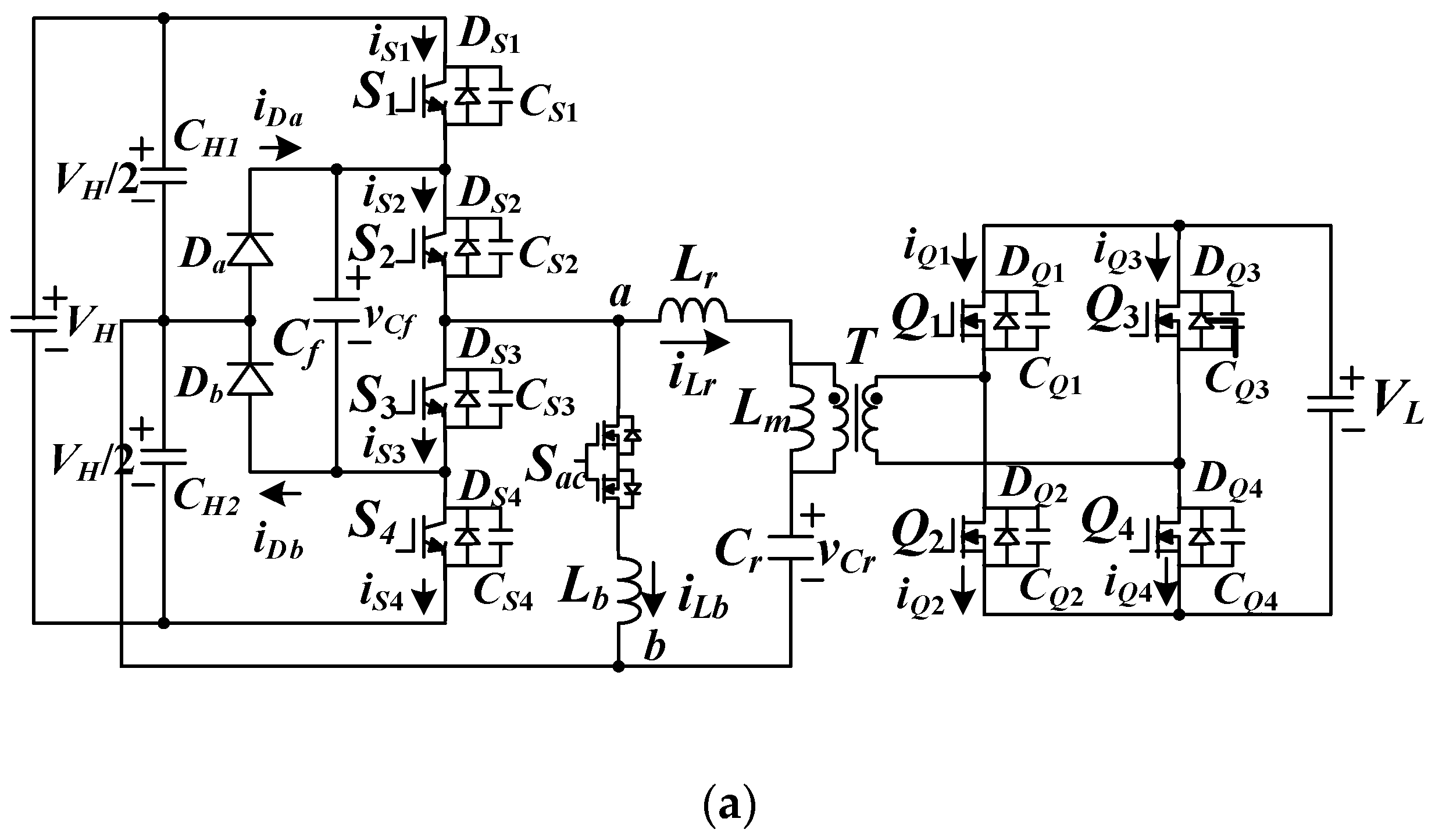
3. Circuit Operation
For forward power delivery, the electric power energy is transferred from
VH side to
VL side and
Sac is OFF.
S1~
S4 are controlled with PFM scheme. Due to PWM signals of
S1~
S4, there is a square wave with −
VH/2 or
VH/2 on the leg voltage
vab. However,
Q1~
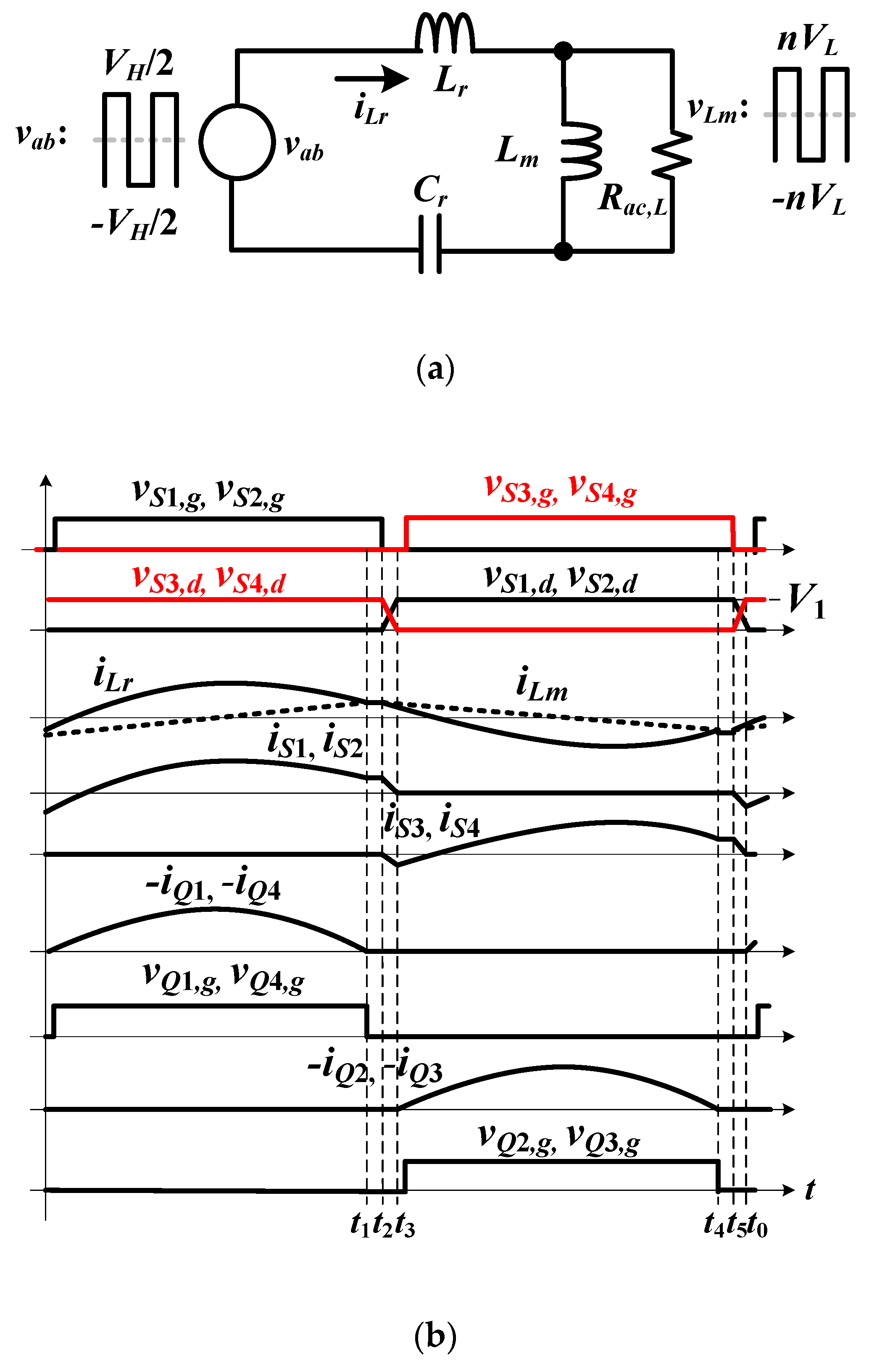
Q4 are operated as the synchronous switches instead of the rectifier diodes in conventional full-bridge rectifier to reduce conduction loss. The equivalent resonant circuit and PWM waveforms for forward power delivery are provided in
Figure 2. To realize the ZVS operation of
S1~
S4, the input impedance of
LLC circuit must be inductive.
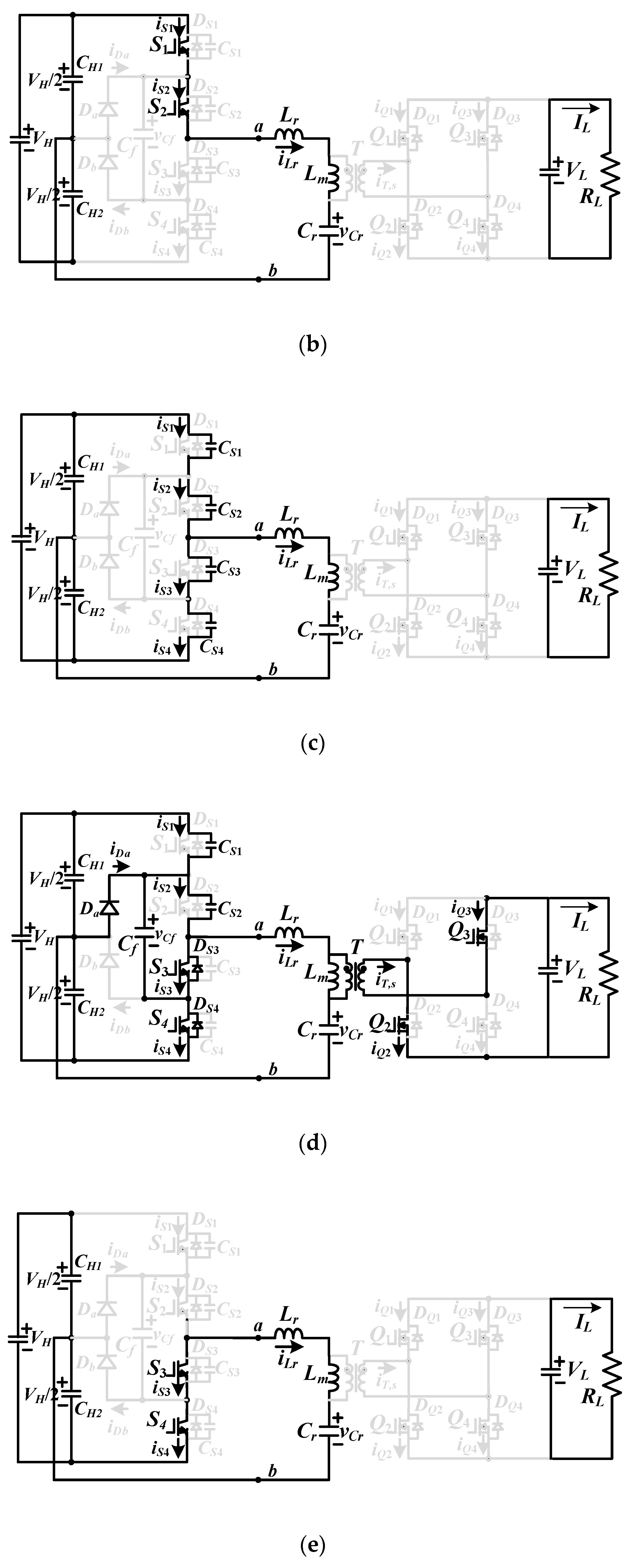
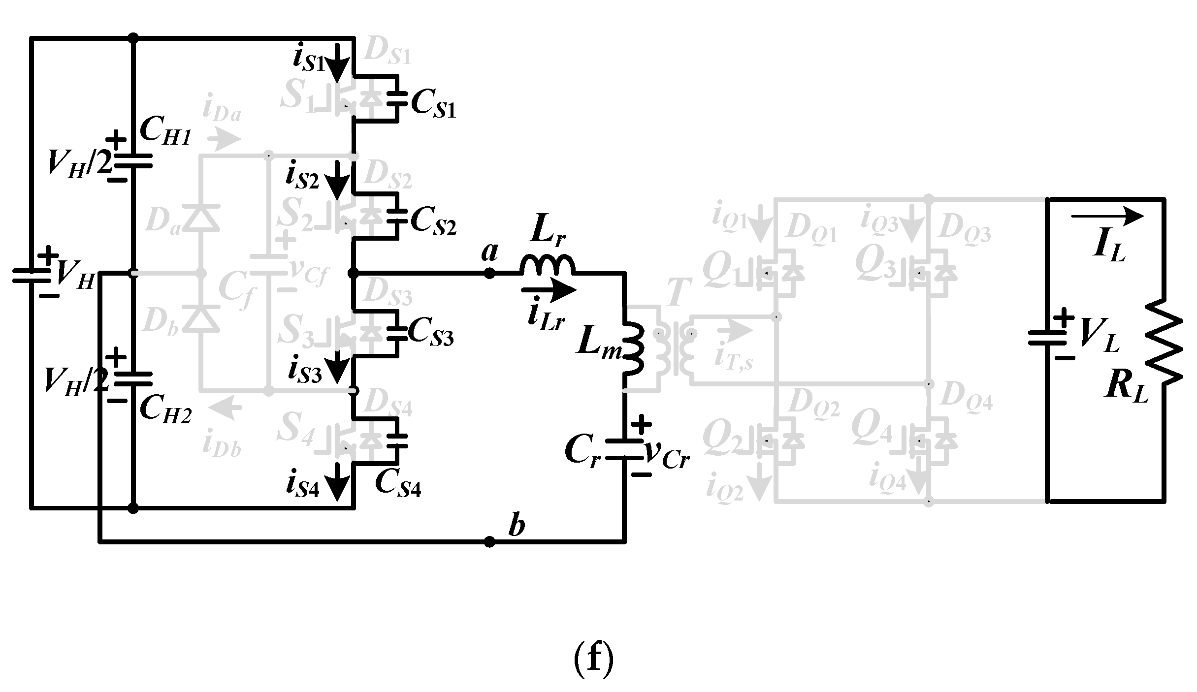
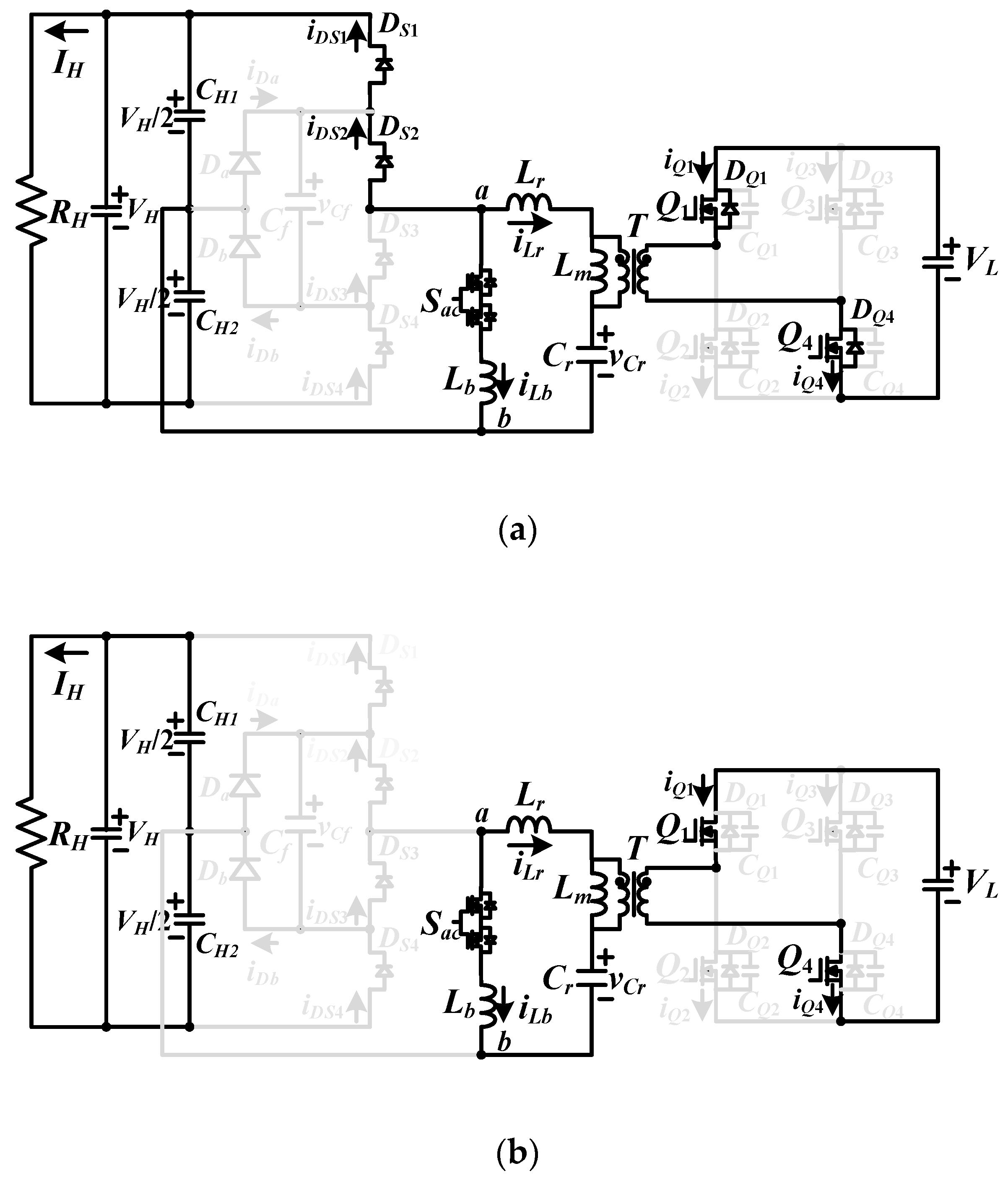
Figure 3 gives the corresponding equivalent circuits related to six operating steps in a switching period under
fr (resonant frequency) >
fsw (switching frequency). It is assumed that the
Lr represents the external series resonant inductance and the leakage inductance of transformer and
Cr represents the external series resonant capacitance and the parasitic capacitance on transformer winding turns. The output capacitances
CS1–
CS4 are assumed to be identical. In the same manner,
CQ1 = … =
CQ4. Since the current
iCf on
Cf is less than
iS1 and
iS2 in mode 1 and
iS3 and
iS4 in mode 4,
iCf is ignored in PWM waveforms. Therefore,
iS1 is equal to
iS2 in steps 1–3 and 6 and
iS3 is equal to
iS4 in steps 3–6.
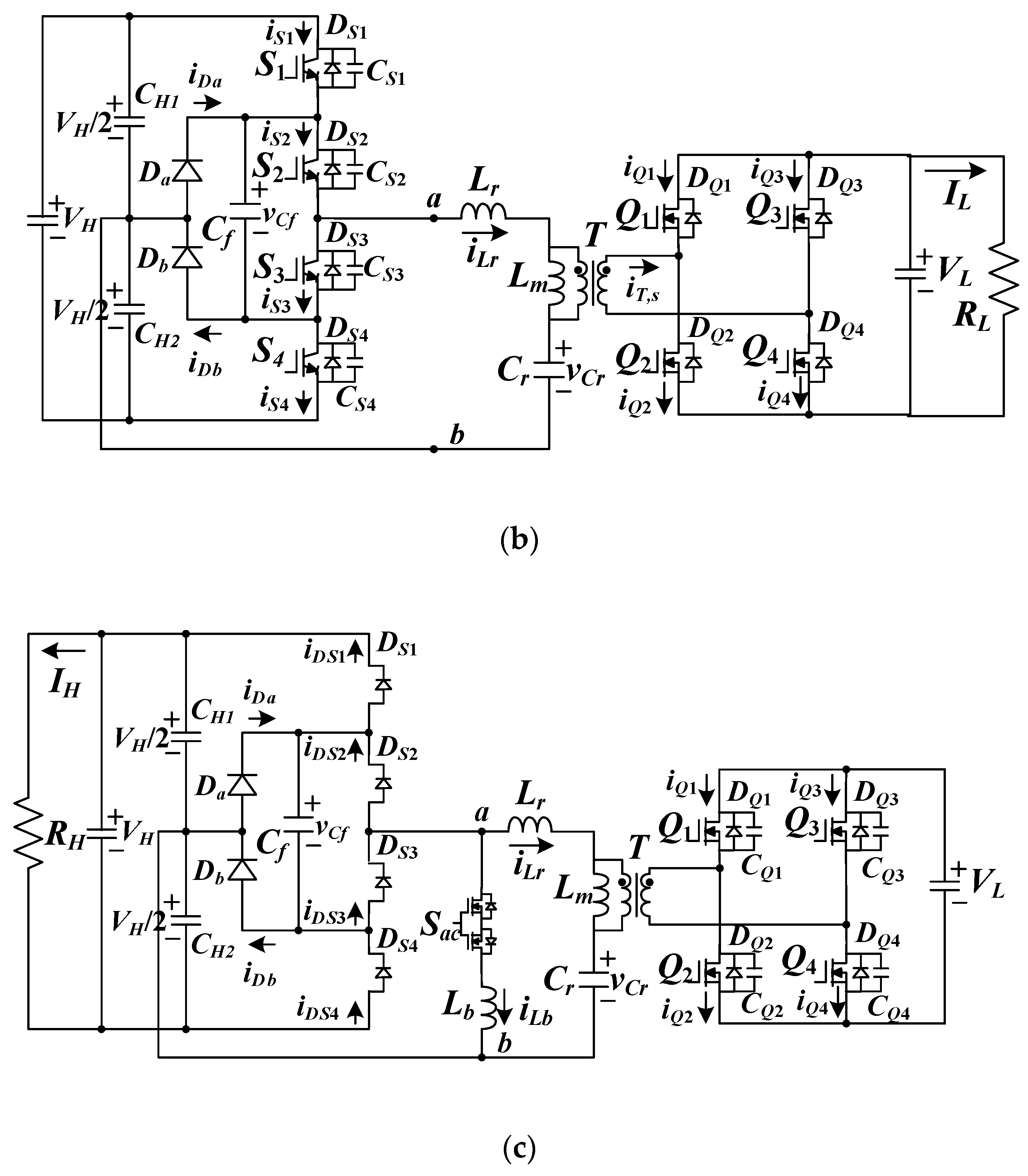
Step 1 (t0 ≤ t < t1): At t < t0, iLr < 0. Thus, iLr discharges CS1 and CS2 are discharged. At t0, vCS1 = vCS2 = 0. Thus, DS1 and DS2 are conducting due to iLr < 0. The ZVS operation of S1 and S2 can be achieved after time t0. If iLr < 0, Db is forward biased. The leg voltage vab = vCf = vCS3 = vCS4 = VH/2. Since iLr > iLm, Q1 and Q4 turn on to conduct the secondary-side current. When iLr increases and iLr > 0, Db becomes off. In this step, the magnetizing voltage vLm is equal to nVL, where n = np/ns is the transformer turns ratio, and iLm increases. The ripple current ΔiLm in step 1 is equal to nVLΔt01/Lm where Δt01 = t1 − t0. The resonant frequency in step 1 is .
Step 2 (t1≤t < t2): If fsw < fr, iQ1 and iQ4 will decrease to zero ampere at t1. Thus, Q1 and Q4 can turn off after time t1. In step 2, the leg voltage vab = VH/2 and Lr, Lm and Cr are resonant.
Step 3 (t2≤t < t3): At
t2,
S1 and
S2 turn off. The positive current
iLr(
t2) will charge
CS1 and
CS2. On the other hand,
CS3 and
CS4 are discharged in this step. The ZVS operation of
S3 and
S4 is expressed in Equation (1).
where
iLm,p is the peak current on
Lm and
CS =
CS1 = … =
CS4. The peak current
iLm,p is calculated from Equation (2).
The dead time
td between
S3 and
S1 (or
S4 and
S2) is approximately expressed in Equation (3).
Therefore, the maximum magnetizing inductance is derived in Equation (4).
Step 4 (t3≤t < t4): At t3, vCS3 = vCS4 = 0. Since iLr(t3) is positive, DS3 and DS4 are conducting. Power devices S3 and S4 can turn on after t3 under zero voltage condition. Since iLr(t3) > 0, Da is forward biased. The leg voltage vab = −VH/2 and vCf = vCS1 = vCS2 = VH/2. When iLr decreases and iLr < 0, Da becomes off. On the secondary side, iQ2(t3) < 0 and iQ3(t3) < 0. Therefore, Q2 and Q3 turn on to conduct the secondary-side current, the primary-side voltage vLm = −nVL and iLm decreases.
Step 5 (t4≤t < t5): The secondary-side switch currents iQ2 = iQ3 = 0 at t4. Then, Q2 and Q3 turn off. In this step, vab = −VH/2 and Lr, Lm and Cr are resonant.
Step 6 (t5≤t <Tsw+t0): At t5, S3 and S4 turn off. In this step, iLr(t5) < 0 and vCS1 and vCS2 decrease. The ZVS condition of S2 and S1 is the same as S4 and S3 in Equation (1). The step 6 is ended at time Tsw+t0.
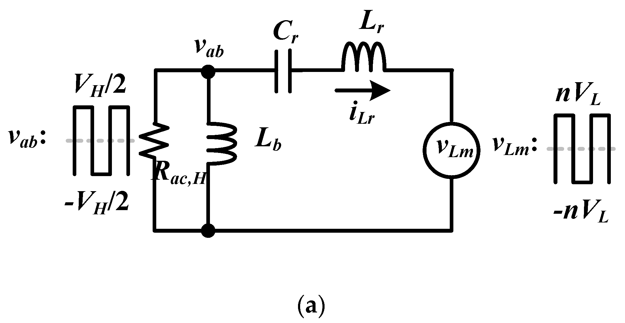
The
LLC resonant circuit is controlled to achieve ZVS operation and the bidirectional power operation. The resonant circuit is based on the fundamental frequency analysis to achieve load voltage regulation. According to the switching status of power devices
S1~
S4 and
Q1~
Q4, the voltage values
VH/2 and −
VH/2 are observed on
vab, and the other voltage values
nVL and −
nVL are generated on the magnetizing inductor voltage
vLm.
Lr,
Cr, Lm and
Rac,L operate as a filter to suppress the high order harmonics. The root mean square (
rms) voltages at the fundamental frequency for input and output sides are
and
. Based on the power balance between the primary-side and the secondary-side of transformer, the primary-side load resistance is expressed as
. The transfer function
GH_L(
s) between the output and input sides in
Figure 2a is obtained as:
where
F = fsw/
fr,
,
K1 = Lm/
Lr and
. From the given input voltage
VH, the output voltage
VL and the circuit parameters
Lr,
Cr,
Lm and
RL, the switching frequency is obtained from Equation (6).
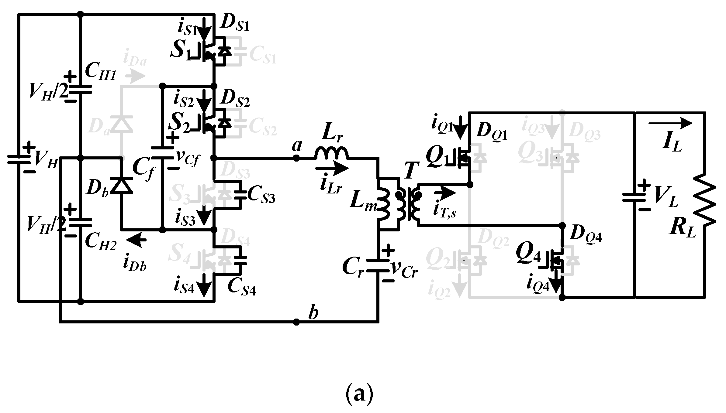
For reverse power flow shown in
Figure 1c, the developed converter transfers power from
VL terminal to
VH terminal.
Sac is turned on and
Lb,
Lr and
Cr are operated as a series resonant circuit to achieve voltage
VH regulation. Power devices
Q1~
Q4 are controlled with PFM scheme and
DS1~
DS4 work as a full-wave rectifier. When |
iLr|>
|iLb|,
DS1 and
DS2 or
DS3 and
DS4 are conducting. Since the
LLC resonant circuit by
Lr,
Cr and
Lb is operated at the inductive load, power devices
Q1~
Q4 are operated at the zero-voltage turn-on switching.
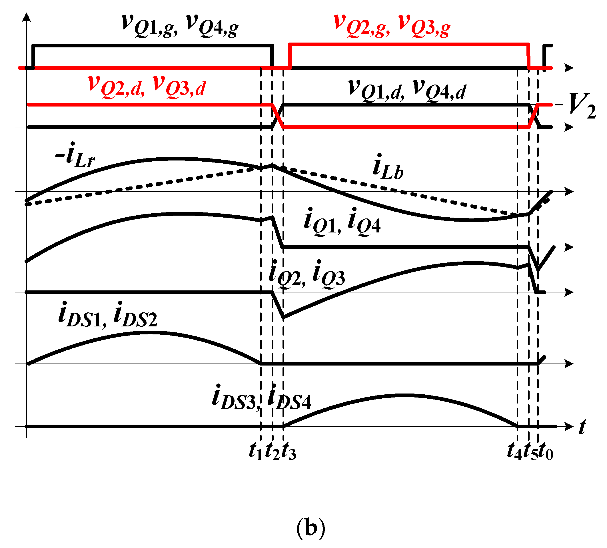
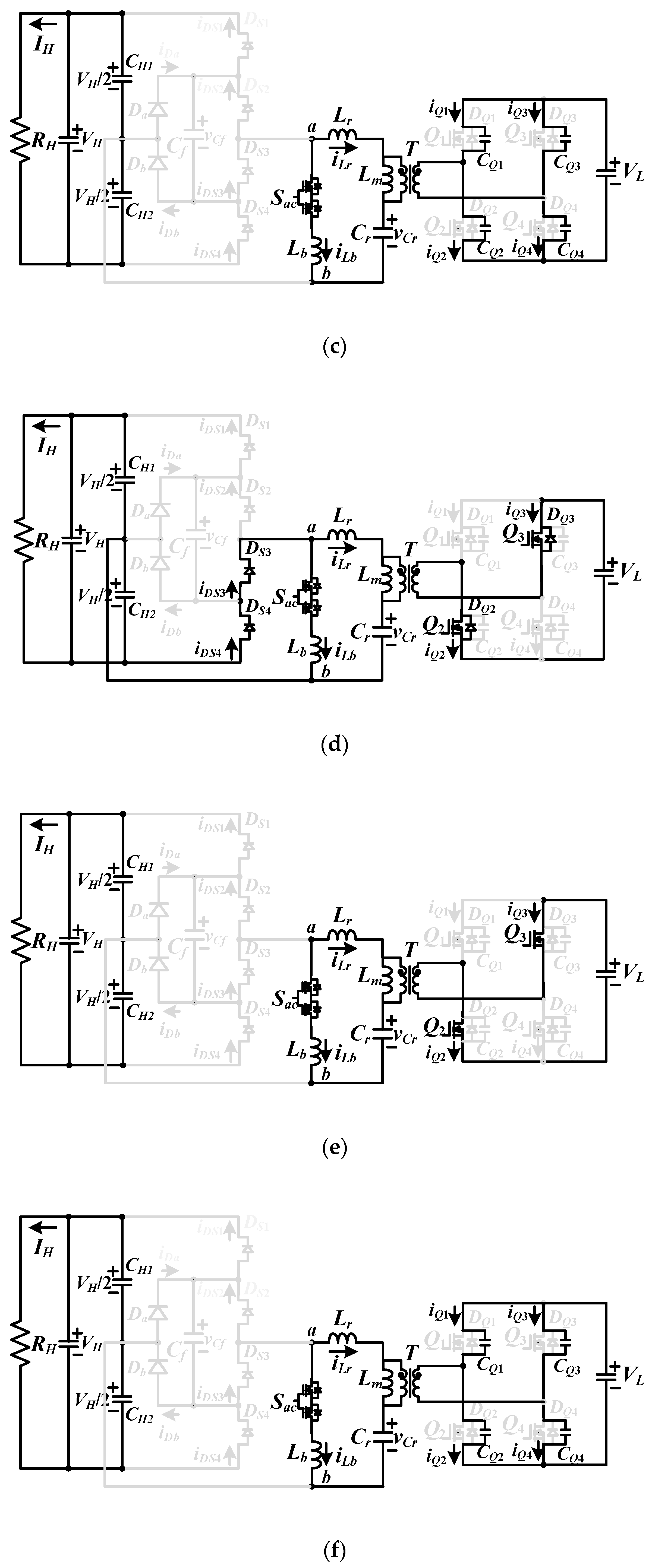
Figure 4a shows the ac equivalent resonant circuit at reverse power flow operation.
Lb and
Rac,H are the parallel inductance and ac equivalent resistance.
Figure 4b gives the main PWM waveforms and
Figure 5 demonstrates the corresponding equivalent circuits at the reverse power flow operation.
Step 1 (t0 ≤ t < t1): This step starts at t0 when vCQ4 = vCQ1 = 0. Then, the DQ4 and DQ1 conduct and vQ2,ds = vQ3,ds = VL. Due to DQ1 and DQ4 are conducting, vQ4,ds and vQ1,ds = 0 and Q1 and Q4 can turn on under zero voltage. Due to iLr(t0) + iLb(t0)<0, DS1 and DS2 are forward biased, CH1 is charged, vLm = nVL, vab = VH/2 and iLm and iLb both increase. Before switches Q1 and Q4 turn off, iDS1 and iDS2 will decrease to zero if fsw < .
Step 2 (t1≤t < t2): At time t1, iDS2 = iDS1 = 0 and DS2 and DS1 are off. Lr, Lb, and Cr are series resonant at frequency .
Step 3 (t2≤t < t3):Q4 and
Q1 turn off at
t2.
CQ2 and
CQ3 are discharged in step 3. The ZVS condition of
Q3 and
Q2 are obtained in Equation (7).
where
CQ =
CQ1 =..=
CQ4,
and
. At
t3, vCQ3(
t3) =
vCQ2(
t3) = 0. The time interval Δ
t23 is expressed in Equation (8).
where
td is dead time between
Q4 and
Q3 or
Q2 and
Q1.
Step 4 (t3≤t < t4): Step 4 starts at t3 when vCQ2 = vCQ3 = 0. Therefore, DQ3 and DQ2 conduct and Q3 and Q2 can turn on under zero voltage. In step 4, DS3 and DS4 conduct, vab = −VH/2, vLm = −nVL, and iLm and iLb both decrease.
Step 5 (t4≤t < t5):iDS3 = iDS4 = 0 at t4. In this step, Q2 and Q3 are still in the on state so that vLm = −nVL. Lb, Cr and Lr are series resonant.
Step 6 (t5≤t < Tsw+t0):Q2 and Q3 turn off at t5. Then, CQ1 and CQ4 are discharged and vCQ1 = vCQ4 = 0 at tsw + t0.
The proposed converter has the similar operation principle for both forward and reverse power operation. For the reverse power operation,
Q1~
Q4 are controlled as main power switches.
DS1~
DS4 are operated as diode rectifier to regulate voltage
VH. The resonant circuit including
Lb,
Lr and
Cr is operated as a filter to suppress high order harmonics. The input
rms voltage at fundamental frequency (
Figure 4a) is calculated as
and the ac equivalent resistance at high voltage side is
. The
rms voltage on
vab is expressed as
. Components
Rac,H,
Lb,
Lr and
Cr are resonant. The transfer function
GL_H(
s) and gain |
GL_H(
s)| are calculated in Equations (9) and (10), respectively.
where
F = fsw/
fr,
,
K2 = Lb/
Lr and
. From the given input voltage
VH, output voltage
VL and the circuit parameters
Lr,
Cr,
Lb and
RH, the switching frequency is obtained from Equation (10).
4. Circuit Parameters and Test Results
For forward power transfer, the input and output voltages are
VH = 750 V to 800 V and
VL = 48 V. The rated power is 1440 W (
vL = 48 V and
IL= 30 A). For reverse power transfer, the input and output voltages are
VL = 36 V to 52 V and
VH = 800 V. The transfer functions in Equations (6) and (10) for forward and backward power transfer operations are similar. Thus, the circuit parameters design operated at forward power flow is presented in this section. The dc voltage gain under
VH = 800 V input and
VL,max = 52 V output is designed to be unity. The transformer turns ratio is calculated in Equation (11).
In the prototype circuit, the selected primary and secondary turns are
nH = 48 and
nL = 6. Thus, the actual transformer turns ratio is
n =
nH/
nL = 8. With the adopted turns ratio, the actual maximum and minimum voltage gains at
VL,nom = 48 V condition are given in Equations (12) and (13).
The control parameters
K1 and
Q1 can be selected at full load
PL,full and minimum input voltage
VH,min conditions. To reduce circulating current, the inductor ratio
K1=10 is used in this prototype circuit. For
Q1 = 0.38 and
K1 = 10, it can obtain the peak gain of |
GH_L(s)| is 1.13. The ac equivalent resistance
Rac,L at the rated power is obtained in Equation (14).
The circuit parameters
and
under
fr = 100 kHz. The actual resonant inductance and capacitance are
Cr = 47 nF and
Lr = 54 µH and the magnetizing inductance
. The theoretical primary
rms current is calculated as:
The theoretical minimum switching frequency is obtained as
. The minimum switching frequency will result in the maximum
rms magnetizing current.
Therefore, the
rms resonant inductor current is obtained in Equation (17).
The flying capacitor
Cf is used to realize voltage balance of
CH1 and
CH2 so that
VCH1 =
VCH2 =
VH/2. The theoretical voltage stresses of power semiconductors can be calculated as
vS1,stress = .. = vS4,stress = VH,max/2
= 400 V and
vQ1,stress = .. = vQ4,stress = VL,max = 52 V. The switch currents approximate
and
. Power devices
S1~
S4 are implemented using IRG4PC40W with 600 V/20 A rating. Power switches
Q1~
Q4 are implemented using IRFB3307 with 75 V/150 A rating.
Sac is implemented using two G20N50C with 500 V/20 A rating. The parallel inductor
Lb is selected as 230 µH and
K2 =
Lb/
Lr = 4.25 under reverse power flow operation. The clamp diodes
Da and
Db are implemented with ultrafast recovery diodes HFA15TB60PBF with 600 V/15 A rating. The other circuit parameters used in the prototype are
CH1 =
CH2 = 330 µF/400 V,
Cf = 2.2 µF/630 V and
CL = 4400 µF/100 V. The parameters and specifications used in the laboratory prototype are given in
Table 1.
Figure 6,
Figure 7,
Figure 8,
Figure 9 and
Figure 10 provide the test results for forward power operation and
Figure 11,
Figure 12,
Figure 13 and
Figure 14 provide the measured waveforms for reverse power operation. The PWM signals of
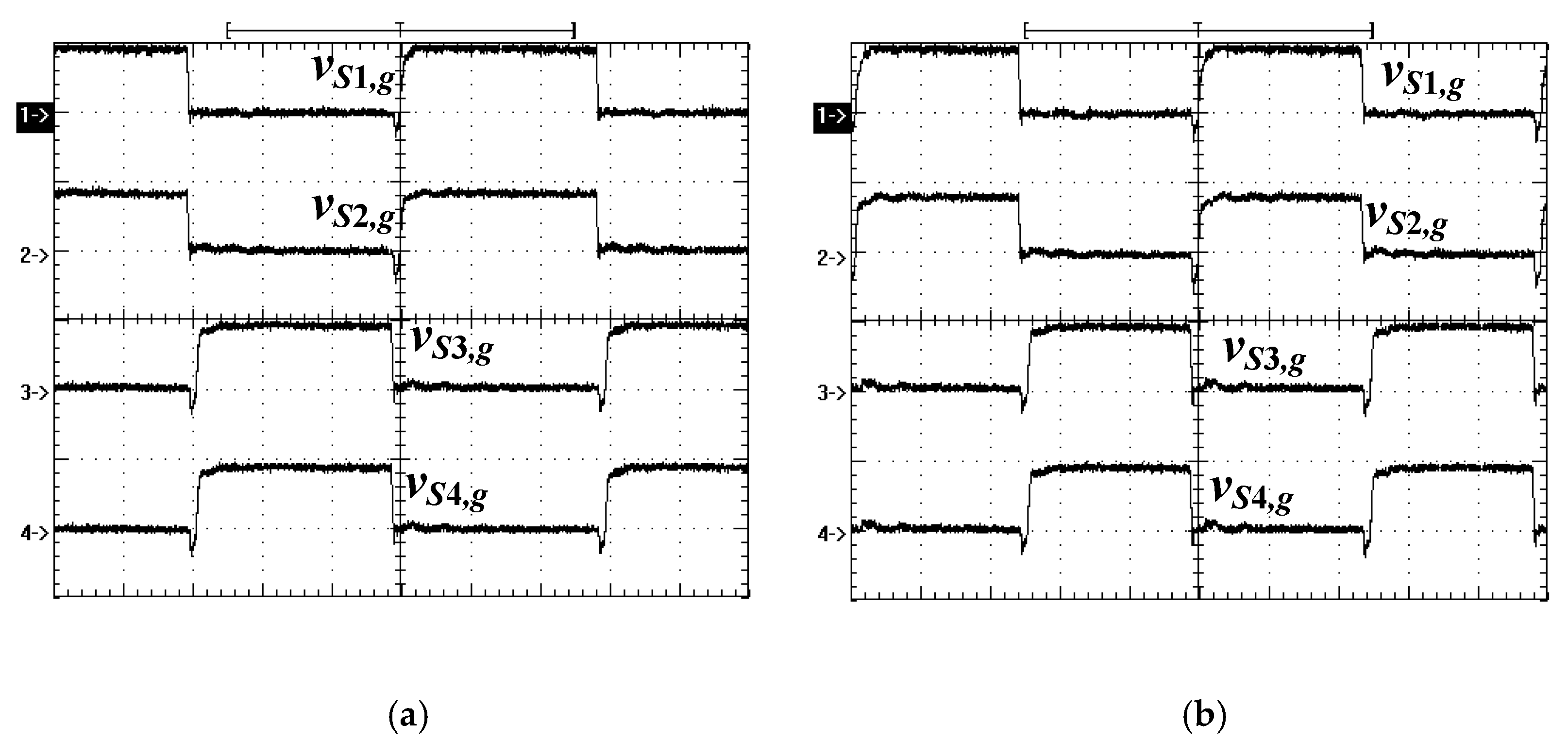
S1–
S4 at 100% load are presented in
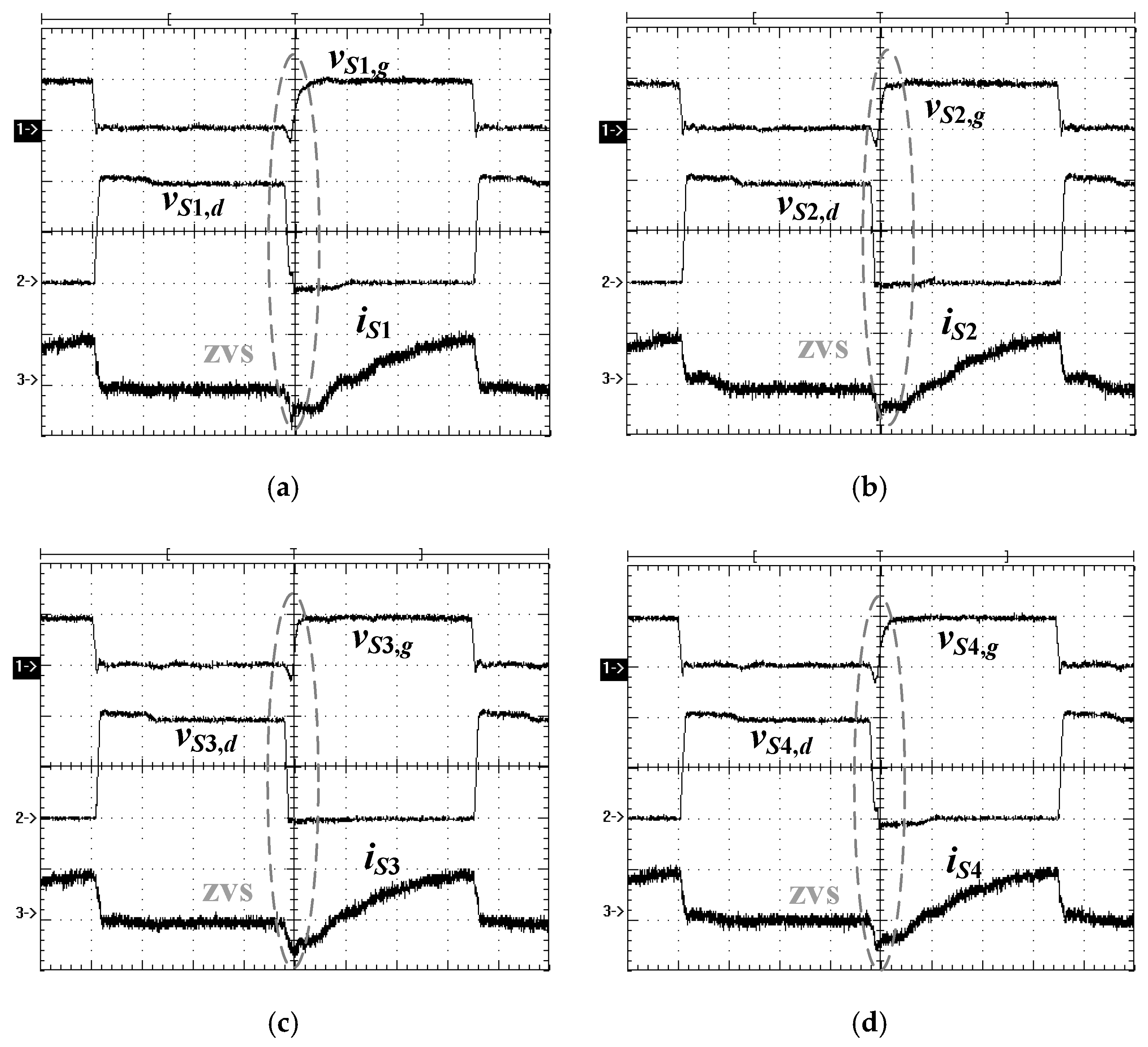
Figure 6.
S1 (
S3) and
S2 (
S4) have the same gate-to-source voltage signals. The converter at
VH = 750 V input has less switching frequency than
VH = 800 V input condition.
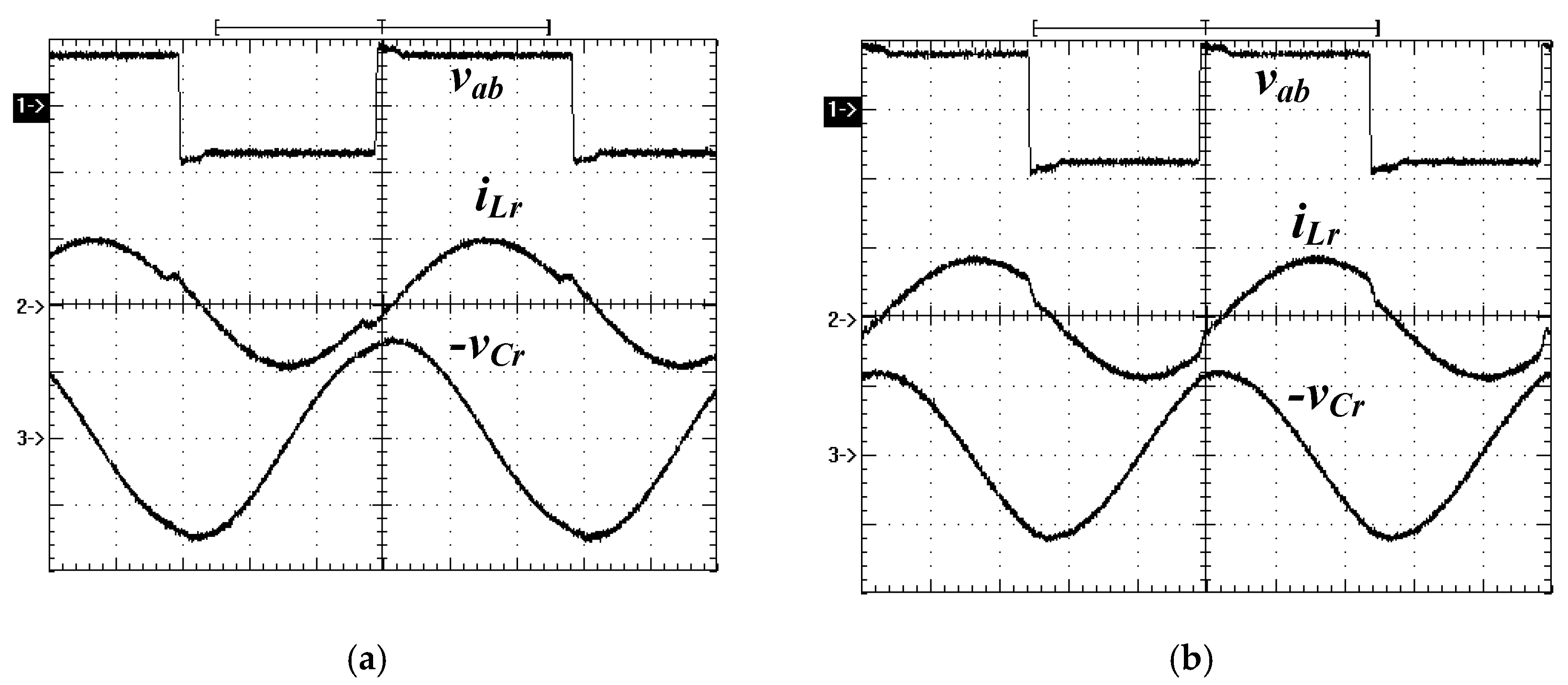
Figure 7 gives the experimental results of leg voltage
vab,
iLr and
vCr at 100% load. It can be seen that the measured waveforms
iLr and
vCr are almost the sinusoidal waves due to
fsw close to
fr for both 750 V and 800 V inputs.
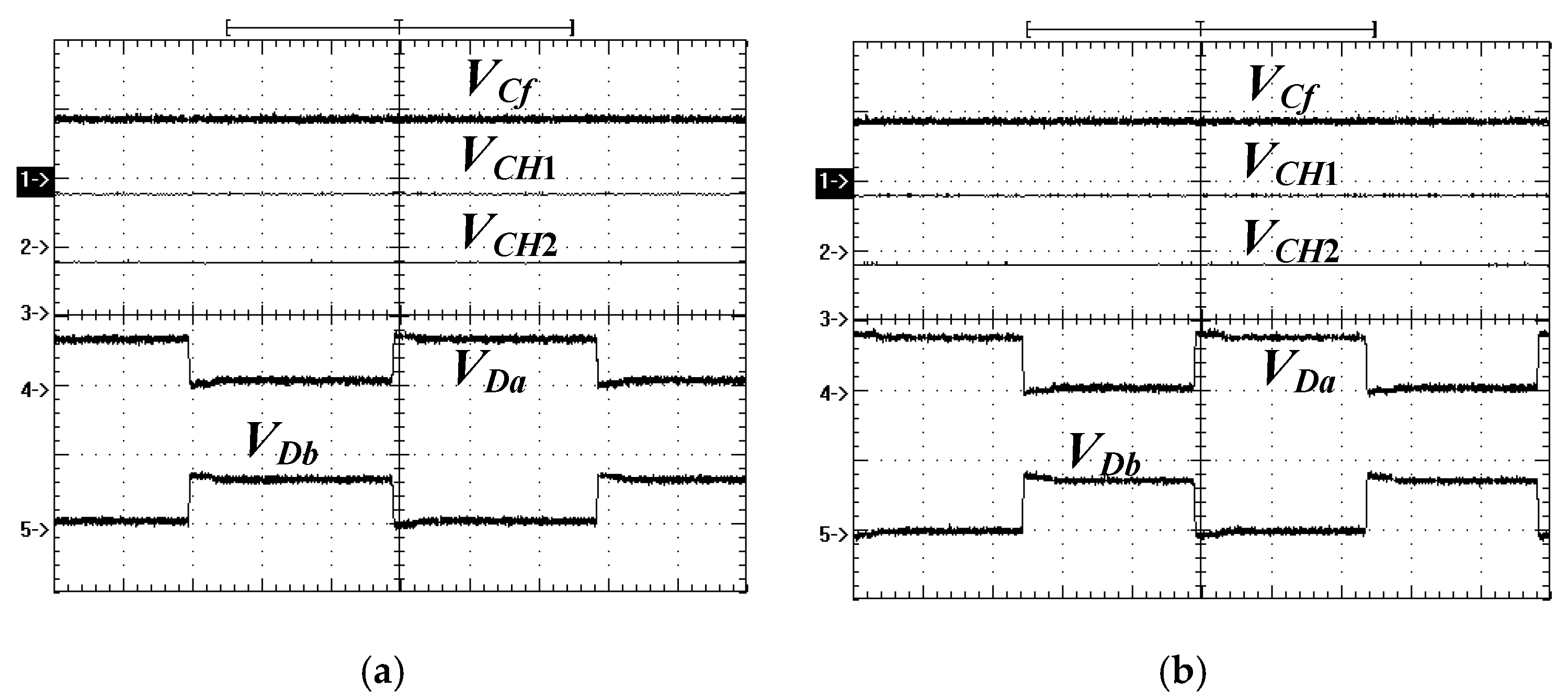
Figure 8 shows the experimental results of
VCH1,
VCH2,
VCf,
VDa and
VDb. The dc voltage differences between
VCH1,
VCH2 and
VCf are about 5V.
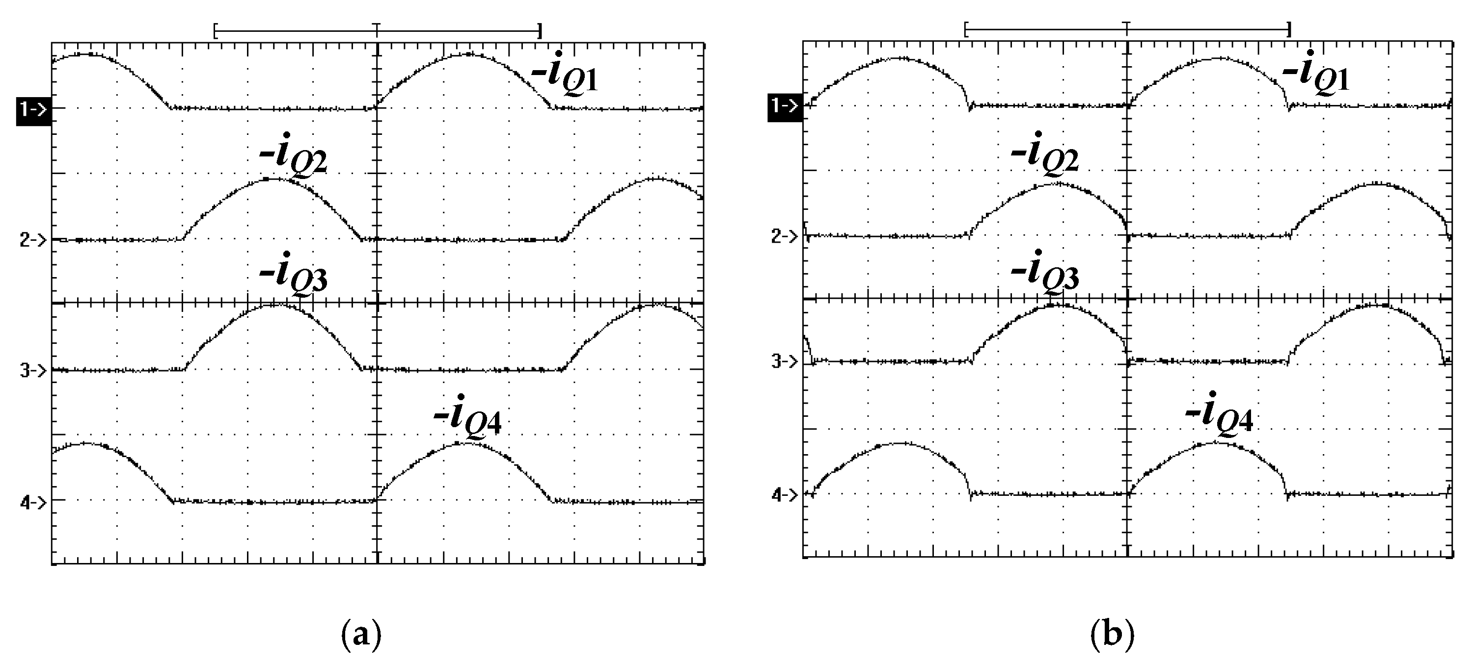
Figure 9 demonstrates the switch currents of
Q1–Q4 at 100% load.
Figure 10 illustrates the PWM waveforms of
S1–
S4 at 20% load. It can observe that
S1–
S4 all turn on under ZVS at 20% load.
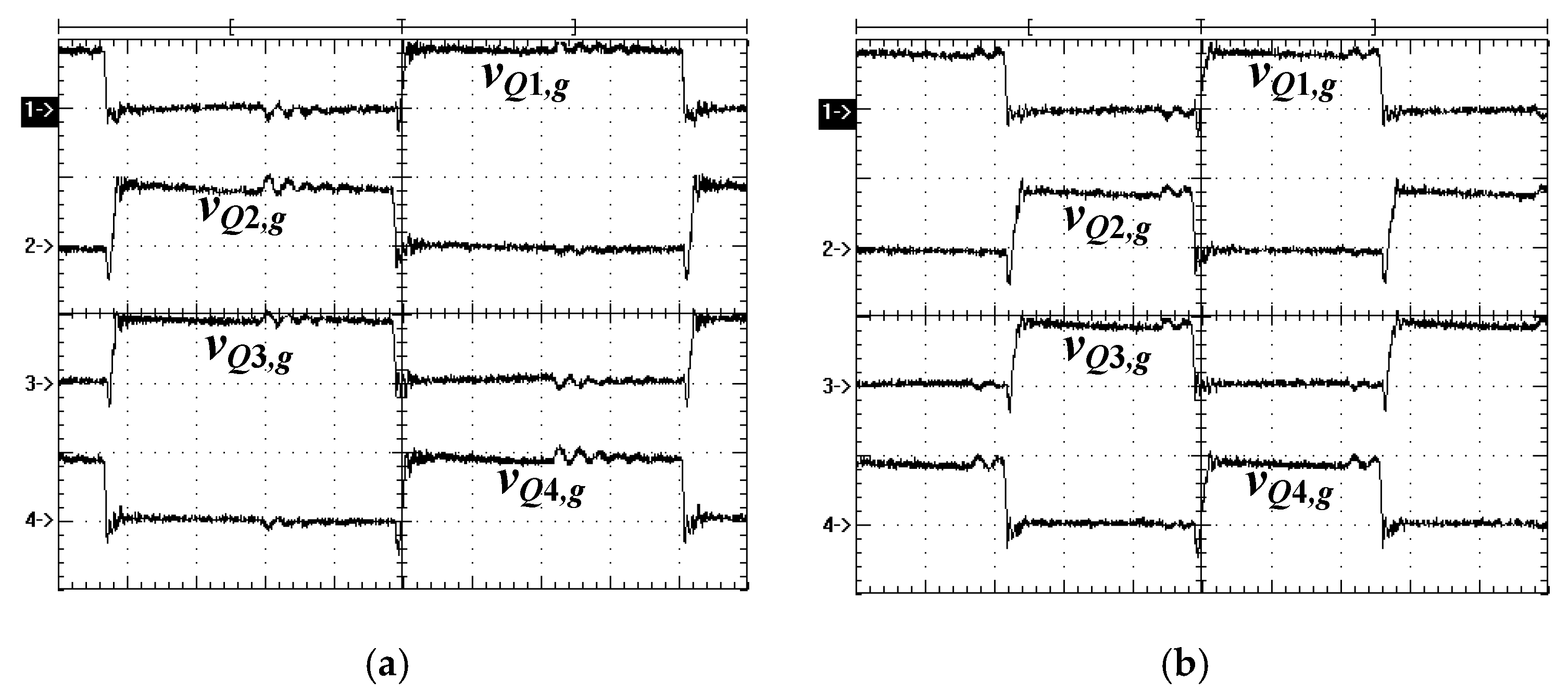
Figure 11 gives the PWM signals of
Q1~
Q4 under backward power operation and different input voltages. Power devices
Q1 (
Q2) and
Q4 (
Q3) have the same gate-to-source voltage signals.
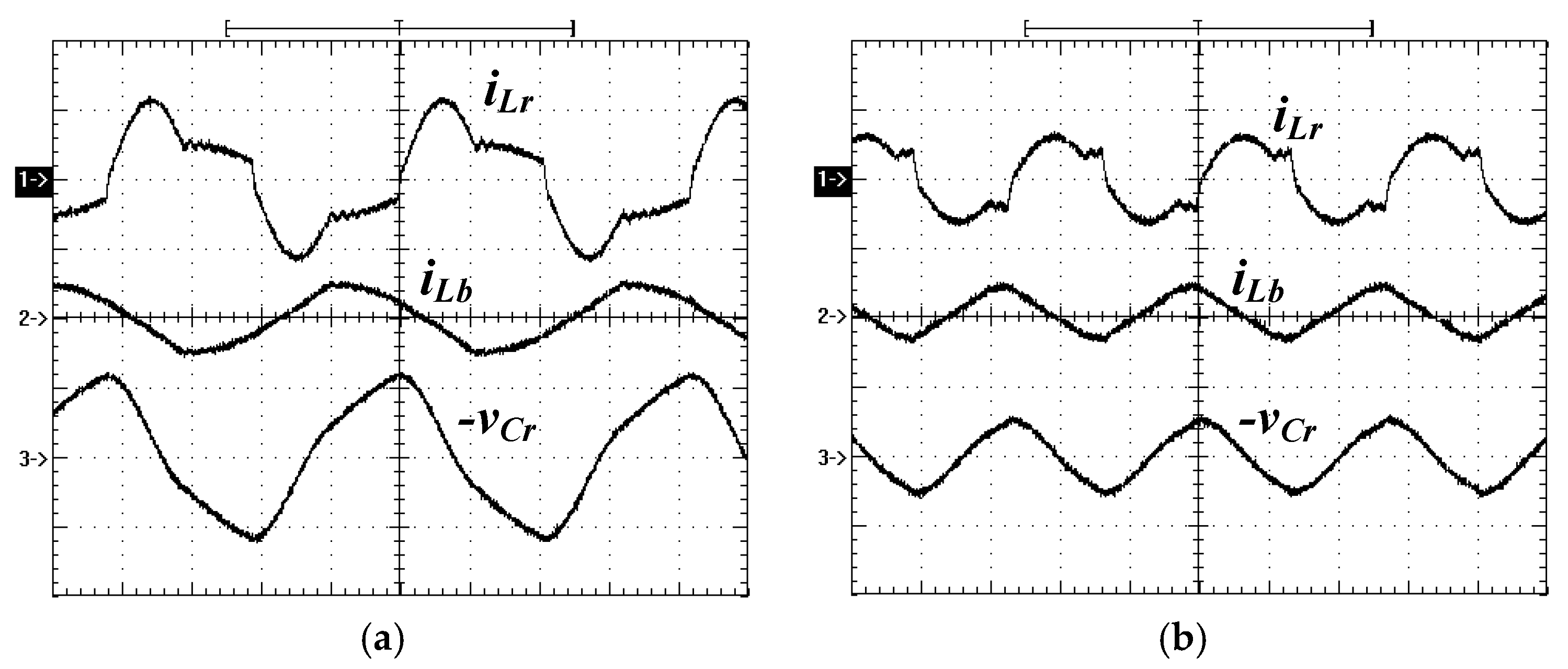
Figure 12 illustrates the measured results of
iLr,
iLb and
vCr under for reverse power operation. The parallel inductor current
iLb is similar to the magnetizing current on conventional
LLC resonant converter to achieve voltage step-up capability.
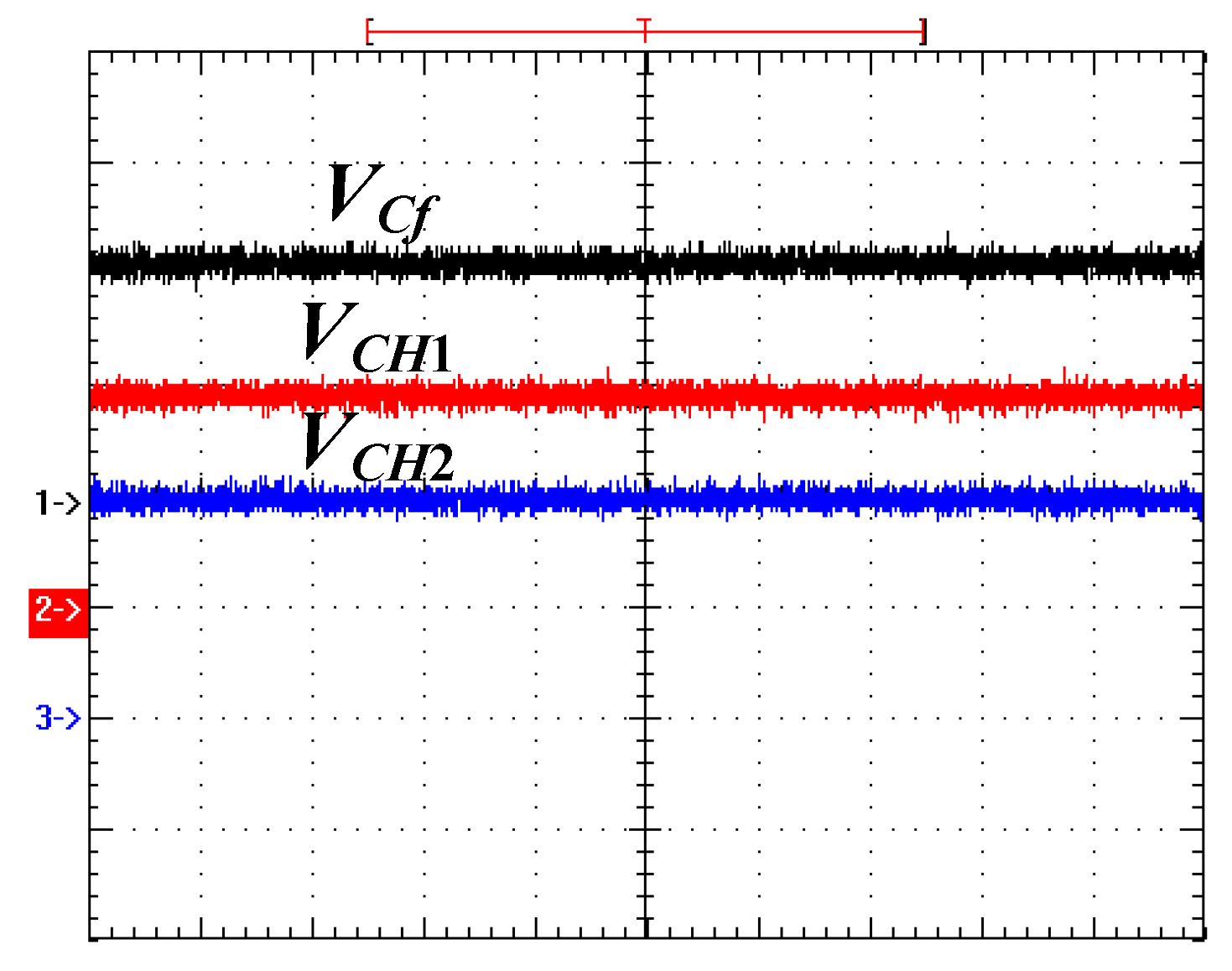
Figure 13 shows the measured capacitor voltages
VCf,
VCH1 and
VCH2 on the high voltage side. These three voltages
VCH1,
VCH2 and
VCf are almost balanced with about 7 V voltage difference.
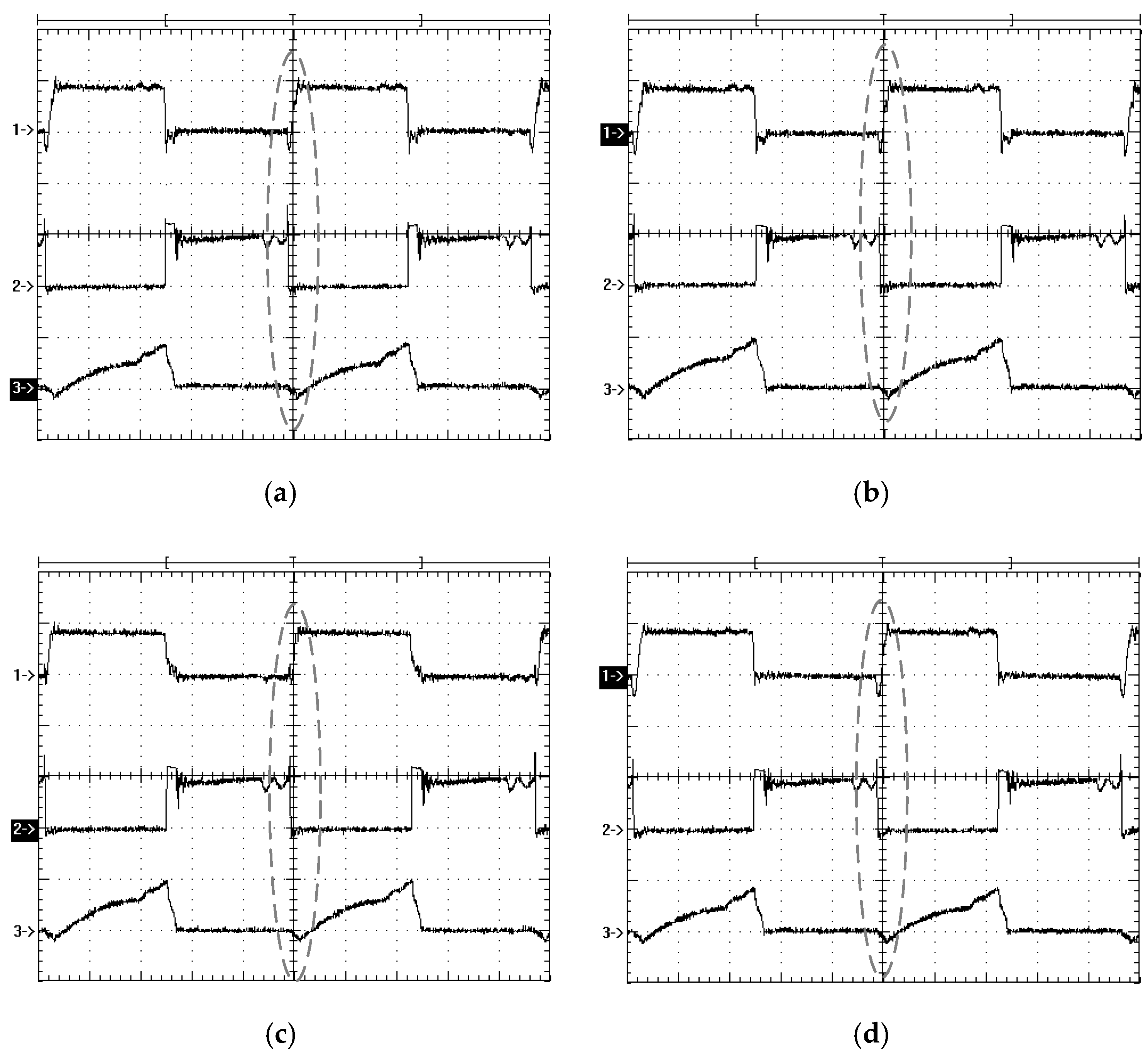
Figure 14 gives the measured PWM waveforms of
Q1~
Q4 under 20% load. It can observe that
Q1–
Q4 can turn on under zero voltage at 20% load. For forward power operation (buck mode), the measured circuit efficiencies are 89.7% at 20% load, 92.1% at 50% load and 91.8% at 100% load under 800 V input. For reverse power operation (boost mode), the measured circuit efficiencies are 86.3% at 20% load, 89.4% at 50% load and 88.9% at 100% load under 40 V input case.
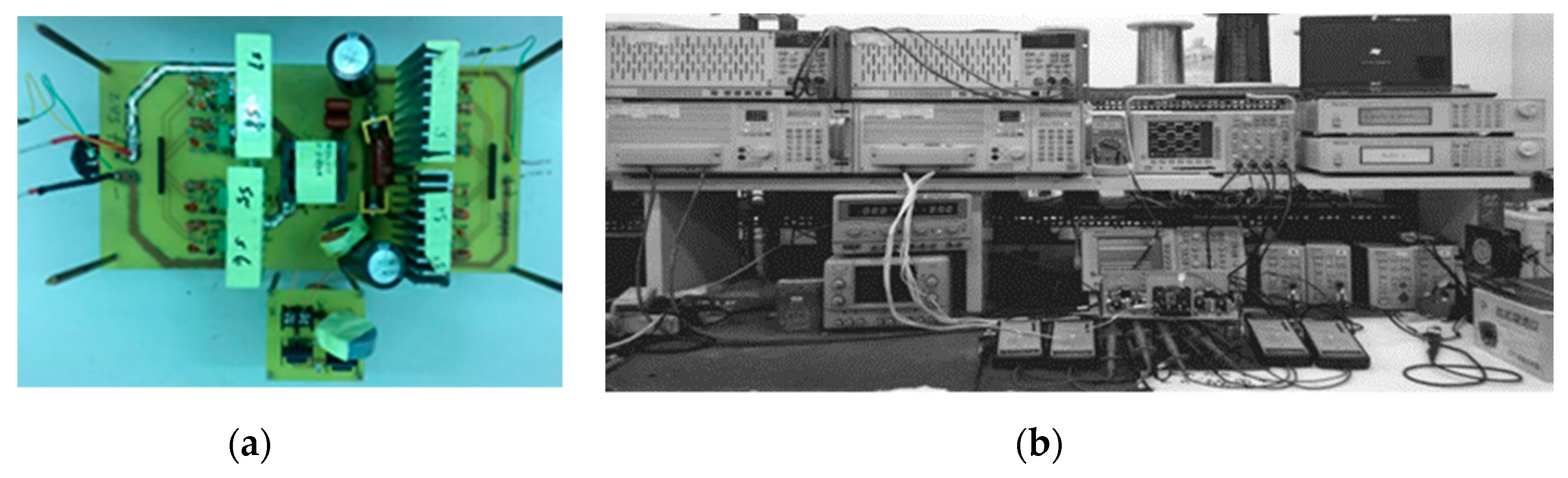
Figure 15a gives the picture of the prototype circuit and the experimental setup is given in
Figure 15b.


