Article

Active Clamp Boost Converter with Blanking Time Tuning Considered

1
Department of Ph.D. Program, Prospective Technology of Electrical Engineering and Computer Science, Department of Electrical Engineering, National Chin-Yi University of Technology, Taichung 41170, Taiwan
2
Department of Electrical Engineering, National Taipei University of Technology, Taipei 10608, Taiwan
*
Author to whom correspondence should be addressed.
Appl. Sci. 2021, 11(2), 860; https://doi.org/10.3390/app11020860
Submission received: 11 December 2020 / Revised: 14 January 2021 / Accepted: 15 January 2021 / Published: 18 January 2021
(This article belongs to the Special Issue Resonant Converter in Power Electronics Technology)

Abstract

:
An active clamp boost converter with blanking time auto-tuned is presented herein, and this is implemented by an additional auxiliary switch, an additional resonant inductor, and an additional active clamp capacitor as compared with the conventional boost converter. In this structure, both the main and auxiliary switches have zero voltage switching (ZVS) turn-on as well as the output diode has zero current switching (ZCS) turn-off, causing the overall efficiency of the converter to be upgraded. Moreover, as the active clamp circuit is adopted, the voltage spike on the main switch can be suppressed to some extent whereas, because of this structure, although the input inductor is designed in the continuous conduction mode (CCM), the output diode can operate with ZCS turn-off, leading to the resonant inductor operating in the discontinuous conduction mode (DCM), hence there is no reverse recovery current during the turn-off period of the output diode. Furthermore, unlike the existing soft switching circuits, the auto-tuning technique based on a given look-up table is added to adjust the cut-off time point of the auxiliary switch to reduce the current flowing through the output diode, so that the overall efficiency is upgraded further. In this paper, basic operating principles, mathematic deductions, potential designs, and some experimental results are given. To sum up, the novelty of this paper is ZCS turn-off of the output diode, DCM operation of the resonant inductor, and auto-tuning of cut-off time point of the auxiliary switch. In addition, the efficiency of the proposed converter can be up to 96.9%.

1. Introduction

How to obtain a high-power density power supply is becoming more and more attractive in the world. By increasing the switching frequency, the size of magnetic devices and capacitors can be reduced so that high-power density requirements can be achieved. However, for the hard switching to be considered, the higher the switching frequency, the greater the switching loss and the more difficult the heat process. In addition, the switching loss under hard switching is proportional to the switching frequency. Consequently, the problem in high switching frequency is becoming more and more serious, thereby causing resonant and soft-switching converters to develop to reduce the switching loss.
The conventional resonant converter is based on the inductor connected in series with the main switch or the capacitor connected in parallel with the main switch so as to form a resonant loop. As the voltage on or current in the switch is dropped to zero, the switch is switched to achieve zero voltage switching (ZVS) turn-on of the switch or zero current switching (ZCS) turn-off of the switch. Basically, this method can reduce the crossover area of voltage and current of the switch, thereby decreasing the switching loss. However, large voltage and current spikes increase the voltage and current stresses of switches as well as increase the conduction losses. Furthermore, in order to render the output voltage controlled at a desired value, the switching frequency is varied because the resonant time is fixed, causing the design of the filter to be difficult.
As the conventional resonant converter has the demerits mentioned above, the soft-switching converter is presented. The ZVS/ZCS pulse-width-modulation (PWM) converter [1,2,3] has put an auxiliary switch to the resonant loop of the resonant converter to make the resonant time point adjustable, thereby leading to fixed frequency control and making the design of the filter easy. However, the conduction loss is large because the resonant voltage on and current in the circuit elements are large. The operating principle of the ZVT/ZCT converter is that prior to turn-on of the main switch, the auxiliary switch is conducted, and hence the transient resonance occurs. As the voltage on or current in the main switch resonates to zero, the main switch is turned on to achieve ZVT turn-on or ZCT turn-off. As the auxiliary switch in the off-state, no resonance happens, leading to effectively reducing the voltage or current stress as well as conduction loss. In the literature [4,5], although the main switches have ZVS turn-on, the auxiliary switches still operate under hard switching. In the literature [6,7,8], although the main and auxiliary switches have ZVS turn-on, many components lead to an increase in cost. The operating behavior of the ZVZCT converter [9,10,11] is that the auxiliary switch has two transient resonances over one cycle so that the main switch has ZVT turn-on and ZCT turn-off. Indeed, this converter can reduce switching and conduction losses, and no additional voltage and current stresses on components. However, such a converter has complexity in control and a relatively large part count, leading to an increase in cost. Furthermore, as the ZVS or ZVT turn-on is relatively suitable for the metal-oxide-semiconductor field-effect transistor (MOSFET) switch [10], there are many studies on the MOSFET switch with ZVS or ZVT turn-on.
In addition, based on the above-mentioned, the ZVS pulse width modulation (PWM) converter, the ZVT converter, and the ZVZCT converter have individual disadvantages. Accordingly, the active clamp technique is developed, which is composed of an auxiliary switch in series with a capacitor. The work of [12] applies the synchronous rectifier to the ZVS active clamp forward converter to reduce the conduction loss. Another paper [13] applies the soft-switched synchronous rectifier to the ZVS active clamp forward converter to reduce the conduction loss as well as the switching loss. A further paper [14] applies the two-switch active clamp to a forward converter for high input voltage applications. The work of [15] applies the phase-shift control to the dual active clamp forward converter to reduce the conduction loss. The work of [16] utilizes the combination of active clamp and passive clamp to improve the light-load efficiency. A further paper [17] applies the secondary-side resonance scheme to the active clamp flyback converter to shape the primary-side current waveform, and hence to reduce the primary-side root-mean-square (RMS) value. Another paper [18] employs the primary-side digital control to regulate the active lamp flyback converter. The work of [19] applies the bidirectional concept to the ZVT active clamp boost converter. The work of [20] applies a coupled inductor to the ZVS active clamp boost converter. In the work of [21], the improved ZVS topology is applied to the active clamp buck converter. Although the converters shown in [19,20,21] have ZVS or ZVT turn-on of the main switches, the number of components used is large, leading to an increase in cost as well as difficulty in circuit analysis. In addition, in CCM, there is no ZCS turn-off of the output diode, leading to a problem in reverse recovery current created from the output diode, which operates during the turn-off period.
Based on the aforementioned, in this paper, one traditional boost converter along with one auxiliary circuit is presented. This auxiliary circuit is composed of one auxiliary switch, one resonant inductor, and one active clamp capacitor, so that the main switch and the auxiliary switch are turned on with ZVS and the output diode is turned off with ZCS, thereby resulting in upgrading the overall efficiency. Furthermore, the proposed active clamp has a function of voltage clamp, thereby leading to reducing the voltage spike on the main switch to some extent, whereas this structure can also cause the output diode to have ZCS turn-off, thereby removing the reverse recovery current. Above all, the proposed auto-tuning technique of the second blanking time is applied to the proposed circuit to upgrade the overall efficiency further. By the way, the potential application of the proposed soft switching converter is for high-power light-emitting diode (LED) lighting fed by the direct current (DC) voltage to improve the overall efficiency [22].

2. Methodology

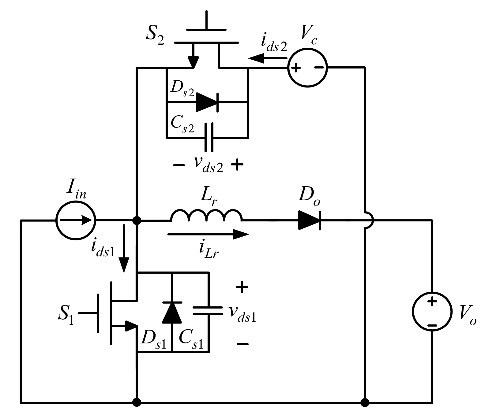
2.1. Proposed Converter

Figure 1 displays the proposed active clamp boost converter, which is constructed by one conventional boost converter combined with one auxiliary circuit. The former is built up by one input inductor Lin and one main switch S1, along with one body diode Ds1, one parasitic capacitor Cs1, one output diode Do, and one output capacitor Co. The latter is constructed by one auxiliary switch S2 along with one body diode Ds2, one parasitic capacitor Cs2, one resonant inductor Lr, and one active clamp capacitor Cc. The load is represented by one output resistor R. In addition, Figure 2 displays the equivalent circuit of the circuit shown in Figure 1, based on the assumption that the values of Co and Cc are large enough to be regarded as ideal voltage sources, whereas the value of Lin is large enough to be viewed as an ideal current source.

2.2. Operation Principles

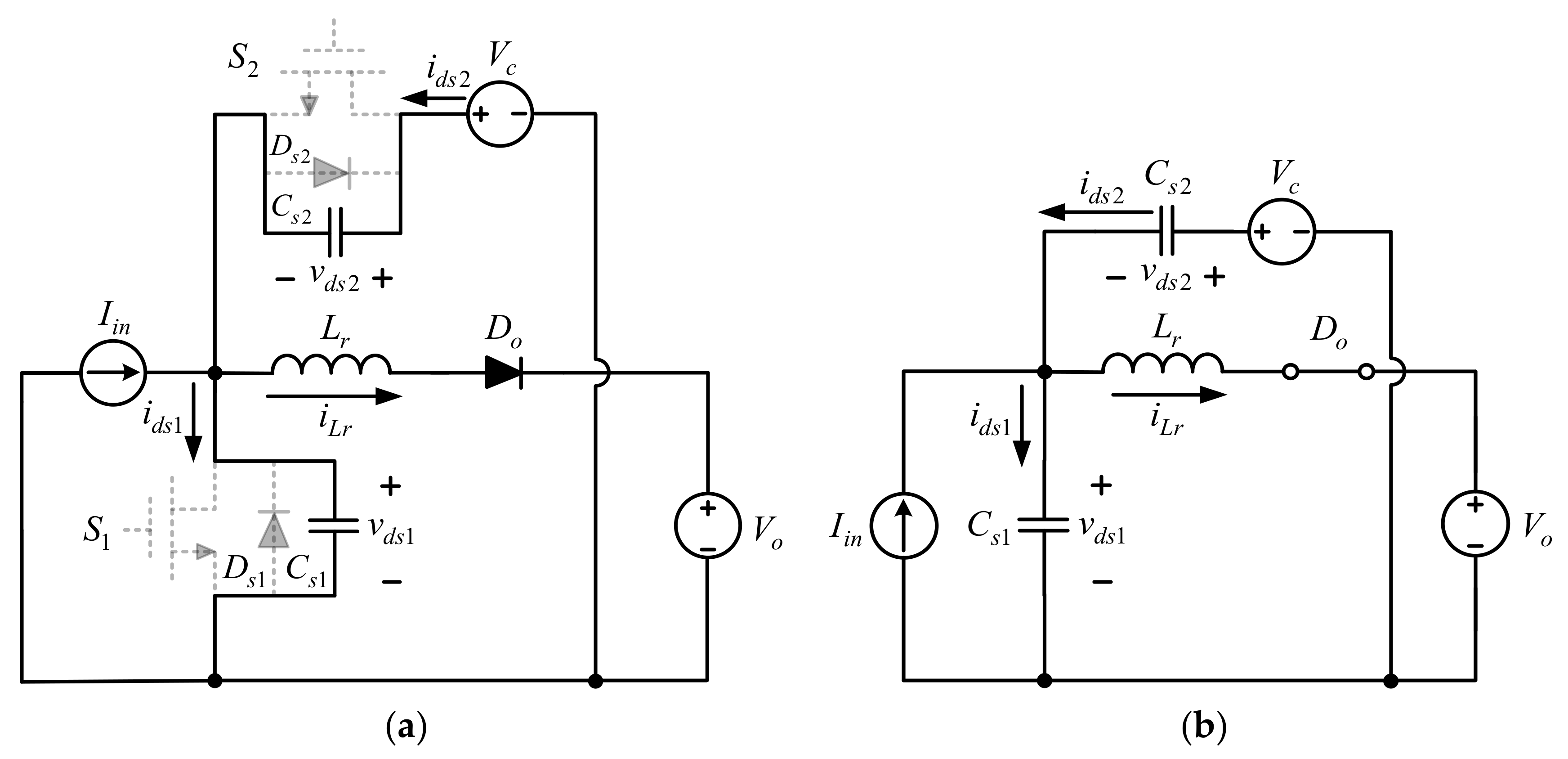
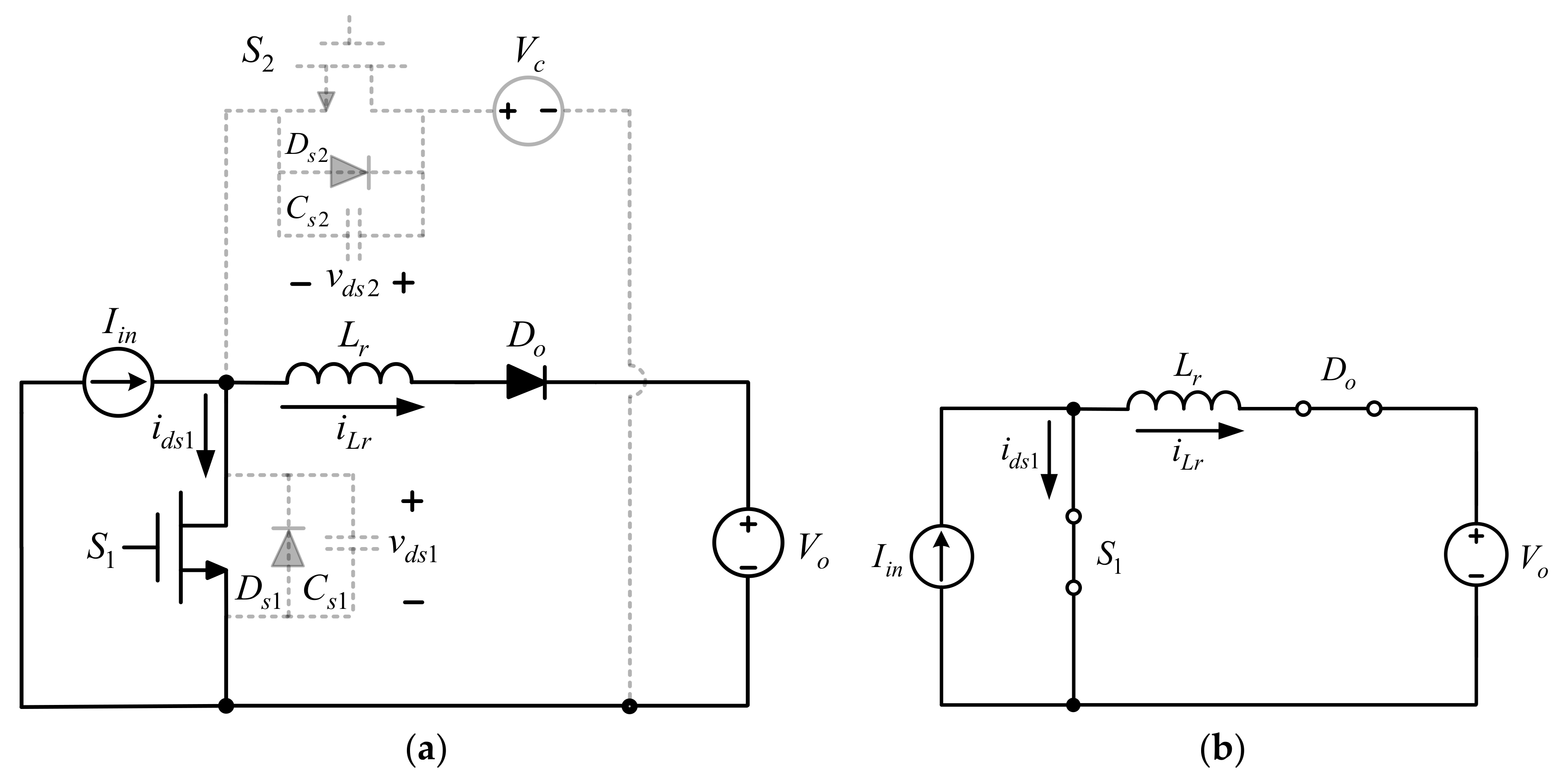
2.2.1. Circuit Behavior

Prior to this section, the symbols and assumptions associated with the circuit displayed in Figure 1 and Figure 2 are given as follows: (i) Vin, Vo, and Vc are the dc input voltage, dc output voltage, and the dc voltage clamp voltage, respectively; (ii) Iin is the dc input current; (iii) iLr is the current in Lr and Do; (iv) vds1 and ids1 are the voltage on and current in S1, respectively; (v) vds1 and ids2 are the voltage on and current in S2, respectively; and (vi) all the elements are ideal except that switches have individual body diodes and parasitic capacitors. There are nine stages in the converter operating shown in Figure 3, where ton is the turn-on time of vgs1, which is equal to DTs with a switching period of Ts and a duty cycle of D, whereas toff is the turn-off time of vgs1, which is equal to (1−D)Ts.

Stage 1: ( t 0 t t 1 )

As illustrated in Figure 3 and Figure 4, S1 is ON but S2 is OFF. During this stage, Lin is magnetized by Vin. At the same time, vds2 is clamped at Vc. Once S1 is cut off, the operation moves to stage 2.

Stage 2: ( t 1 t t 2 )

As illustrated in Figure 3 and Figure 5, S1 is cut off and S2 is still OFF. During this state, Cs1 is abruptly charged to Vc. As Vc = vds1 + vds2, Cs2 is abruptly discharged to zero. At the same time, Lr is magnetized and the energy at input terminal is transferred to the output terminal via Do. Once the energy stored in Cs2 is entirely exhausted, the operation proceeds to stage 3.
According to Figure 5b, three stage equations can be obtained as
I i n = C s 1 d v d s 1 ( t ) d t + i L r ( t ) C s 2 d v d s 2 ( t ) d t V c = v d s 1 ( t ) + v d s 2 ( t ) v d s 1 ( t ) = L r d i L r ( t ) d t + V o
By assuming that two switches are identical, Cs1 = Cs2 = Cs. Moreover, the initial values of this stage are iLr(t1) = 0, vds1(t1) = 0 and vds2(t1) = Vc. By taking the Laplace transform of Equation (1), the following equations can be attained to be
I L r ( s ) = ( 1 s s s 2 + 1 2 L r C s ) I i n ( 1 L r s 2 + 1 2 L r C s ) V o V d s 1 ( s ) = ( 1 s s s 2 + 1 2 L r C s ) V o + ( 1 2 C s s 2 + 1 2 L r C s ) I i n V d s 2 ( s ) = V c s ( 1 s s s 2 + 1 2 L r C s ) V o ( 1 2 C s s 2 + 1 2 L r C s ) I i n
By taking the inverse Laplace transform of Equation (2), the following equations can be attained to be
i L r ( t ) = I i n [ 1 cos   ω 1 ( t t 1 ) ] V o Z 1 sin   ω 1 ( t t 1 ) v d s 1 ( t ) = V o [ 1 cos   ω 1 ( t t 1 ) ] + I i n Z 1 sin   ω 1 ( t t 1 ) v d s 2 ( t ) = V c V o [ 1 cos   ω 1 ( t t 1 ) ] I i n Z 1 sin   ω 1 ( t t 1 )
where
ω 1 = 1 2 L r C s   and   Z 1 = L r 2 C s
If ω 1 ( t t 1 ) 0 , then cos   ω 1 ( t t 1 ) and sin   ω 1 ( t t 1 ) can be close to the following equations:
cos   ω 1 ( t t 1 ) 1 sin   ω 1 ( t t 1 ) ω 1 ( t t 1 )
Substituting Equation (5) into Equation (3) yields
v d s 2 ( t ) V c I i n Z 1 ω 1 ( t t 1 )
According to Equation (6) and vds(t2) = 0, the corresponding time elapsed T2 is
T 2 = t 2 t 1 = 1 ω 1 ( V c I i n Z 1 )

Stage 3: ( t 2 t t 3 )

As illustrated in Figure 3 and Figure 6, S1 and S2 are both still OFF. In the previous stage, vds1(t2) = Vc and vds2(t2) = 0. During this stage, iLr is smaller than Iin. Hence, DS2 is conducted, making vds1 still clamped at Vc. At the same time, the voltage across Lr is VcVo, causing iLr to increase linearly. As soon as S2 is conducted, the operation goes to stage 4.
According to Figure 6b, one stage equation can be obtained as
L r d i L r ( t ) d t = V c V o
As the initial value of this stage is iLr(t2) = ILr2, solving Equation (8) yields
i L r ( t ) = ( V c V o ) L r ( t t 2 ) + I L r 2
Since iLr(t3) = ILr3, the corresponding time elapsed T3 is
T 3 = t 3 t 2 = ( I L r 3 I L r 2 ) V c V o L r

Stage 4: ( t 3 t t 4 )

As illustrated in Figure 3 and Figure 7, S1 is still OFF, but S2 is conducted. In the previous stage, vds2(t3) = 0. Therefore, S2 is conducted at t3 with ZVS. As Iin is still smaller than iLr, the voltage across Lr is still Vc Vo, causing Lr to still be linearly magnetized. Once iLr = Iin, the operation proceeds to stage 5.
One stage equation can be obtained as shown in Figure 7b.
L r d i L r ( t ) d t = V c V o
As the initial value of this stage is iLr(t3) = ILr3, solving Equation (11) yields
i L r ( t ) = ( V c V o ) L r ( t t 3 ) + I L r 3
Because iLr(t4) = Iin, the corresponding time elapsed T4 is
T 4 = t 4 t 3 = ( I i n I L r 3 ) V c V o L r

Stage 5: ( t 4 t t 5 )

As illustrated in Figure 3 and Figure 8, S1 is still OFF, but S2 is still ON. Hence, the voltage across S1 is clamped at Vc. During this stage, iLr is larger than Iin, changing ids2 to the positive direction. At the same time, the voltage across Lr is still Vc Vo, causing Lr to still be linearly magnetized. As soon as S2 is cut off, the operation goes to stage 6.
One stage equation can be obtained as shown in Figure 8b.
L r d i L r ( t ) d t = V c V o
As the initial value of this stage is iLr(t4) = Iin, solving Equation (14) yields
i L r ( t ) = ( V c V o ) L r ( t t 4 ) + I i n
Because iLr(t5) = ILr5, the corresponding time elapsed T5 is
T 5 = t 5 t 4 = ( I L r 5 I i n ) V c V o L r

Stage 6: ( t 5 t t 6 )

As illustrated in Figure 3 and Figure 9, S1 is still OFF and S2 is cut off. During this stage, iLr is still large than Iin, hence Cs2 is abruptly charged to Vc and Cs1 is abruptly discharged to zero. At the same time, Lr begins to be demagnetized. The moment Cs1 is discharged to zero, this stage comes to an end and the next stage begins.
Three stage equations can be obtained as shown in Figure 9b.
I i n = C s 1 d v d s 1 ( t ) d t + i L r ( t ) C s 2 d v d s 2 ( t ) d t V c = v d s 1 ( t ) + v d s 2 ( t ) v d s 1 ( t ) = L r d i L r ( t ) d t + V o
By assuming two switches are identical, Cs1 = Cs2 = Cs. Further, the initial values of this stage are iLr(t5) = ILr5, vds1(t5) = Vc and vds2(t5) = 0. Based on Equation (4) and by taking the Laplace transform of Equation (17), the following equations can be attained:
I L r ( s ) = I i n s s s 2 + 1 2 L r C s ( I i n I L r 5 ) + 1 L r s 2 + 1 2 L r C s ( V c V o ) V d s 1 ( s ) = V o s + s s 2 + 1 2 L r C s ( V c V o ) + 1 2 C s s 2 + 1 2 L r C s ( I i n I L r 5 ) V d s 2 ( s ) = V c s V o s s s 2 + 1 2 L r C s ( V c V o ) 1 2 C s s 2 + 1 2 L r C s ( I i n I L r 5 )
By taking the inverse Laplace transform, the following equations can be attained:
i L r ( t ) = I i n ( I i n I L r 5 )   cos   ω 1 ( t t 5 ) + ( V c V o ) Z 1   sin   ω 1 ( t t 5 ) v d s 1 ( t ) = V o + ( V c V o )   cos   ω 1 ( t t 5 ) + ( I i n I L r 5 ) Z 1   sin   ω 1 ( t t 5 ) v d s 2 ( t ) = V c V o ( V c V o )   cos   ω 1 ( t t 5 ) ( I i n I L r 5 ) Z 1   sin   ω 1 ( t t 5 )
According to Equations (5) and (19), the equation of vds2(t) can be simplified to
v d s 2 ( t ) ( I L r 5 I i n ) Z 1 ω 1 ( t t 5 )
According to Equation (20) and vds2(t6) = Vc, the corresponding time elapsed T6 is
T 6 = t 6 t 5 = 1 ω 1 [ V c ( I L r 5 I i n ) Z 1 ]

Stage 7: ( t 6 t t 7 )

As illustrated in Figure 3 and Figure 10, S1 and S2 are still OFF, In the previous stage, vds1 is equal to zero, whereas vds2 is equal to Vc. During this stage, iLr is still larger than Iin, making Ds1 conducted, hence vds2 still clamped at Vc. At the same time, the voltage across Lr is Vo, causing Lr to be linearly demagnetized. As soon as S1 is conducted, this stage comes to an end and the next stage begins.
According to Figure 10b, one stage equation can be obtained as
L r d i L r ( t ) d t = V o
As the initial value of this stage is iLr(t6) = ILr6, solving Equation (22) yields
i L r ( t ) = I L r 6 V o L r ( t t 6 )
Because iLr(t7) = ILr7, the corresponding time elapsed T7 is
T 7 = t 7 t 6 = ( I L r 6 I L r 7 ) V o L r

Stage 8: ( t 7 t t 8 )

As illustrated in Figure 3 and Figure 11, S1 is conducted and S2 is still OFF. In the previous stage, Ds1 is conducted so S1 is switched on with ZVS at t7. As iLr is still larger than Iin, the voltage across Lr is still Vo, causing Lr to be still linearly demagnetized. As iLr = Iin, this stage ends and the next stage starts.
According to Figure 11b, one stage equation can be obtained as
L r d i L r ( t ) d t = V o
As the initial value of this stage is iLr(t7) = ILr7, solving Equation (25) yields
i L r ( t ) = i L r 7 V o L r ( t t 7 )
Because iLr(t8) = Iin, the corresponding time elapsed T8 is
T 8 = t 8 t 7 = ( I L r 7 I i n ) V o L r

Stage 9: ( t 8 t t 0 + T s )

As illustrated in Figure 3 and Figure 12, S1 is still ON but S2 is still OFF. Hence, vds2 is clamped at Vc. During this stage, iLr is smaller than Iin, changing ids1 to the positive direction. At the same time, the voltage across Lr is Vo, causing Lr to still be linearly demagnetized. From Figure 3, it can be seen that, as iLr = 0, the output diode Do is cut off before the turn-off time point of vgs1, meaning that Do has ZCS turn-off. Once iLr = 0, this stage ends with the next cycle repeated.
According to Figure 12b, one stage equation can be obtained as
L r d i L r ( t ) d t = V o
As the initial value of this stage is iLr(t8) = Iin, solving Equation (28) yields
i L r ( t ) = I i n V o L r ( t t 8 )
Because iLr(t0 + Ts) = 0, the corresponding time elapsed T9 is
T 9 = t 0 t 8 = I i n V o L r
If T8 plus T9, which is about T9, is smaller than ton, i.e., DTs, the resonant inductor Lr works in DCM, meaning that there is no reverse recovery current during the turn-off period of Do. Because vgs1 and vgs2 have two blanking times between them per cycle, if T9 is larger than ton, then at the instant when S1 is cut off, but S2 is still OFF, iLr will flow through Ds1. Once S2 is turned on, a large reverse recovery current will flow through S2 owing to a reverse voltage of Vc across Ds1. Accordingly, S2 may be destroyed as a result of this current spike or S1 is turned on again, causing shoot-through between S1 and S2.
Table 1 is used to summarize soft switching types in the proposed converter.

2.2.2. Voltage Gain

By applying the voltage-second balance to Lin, we can obtain
1 T s t t + T s v L i n ( τ ) d τ = V i n ( D + α ) + ( V i n V c ) ( 1 D α ) = 0
By rearranging Equation (31), we can obtain
V c V i n = 1 1 D α
where
α = T 6 + T 7 T s
By applying the voltage-second balance to Lr, we can obtain
1 T s t t + T s v L r ( τ ) d τ = ( V c V o ) ( 1 D α ) + ( V o ) ( α + β ) = 0
By rearranging Equation (34), we can obtain
V o V c = 1 D α 1 D + β
where
β = T 8 + T 9 T s
Substituting Equation (35) into Equation (32) yields
V o V i n = 1 1 D + β
It can be seen from Equation (35) that the active clamp voltage Vc is larger than the output voltage Vo, whereas it can also be seen from Equation (37) that this voltage gain is smaller than that of the conventional boost converter in CCM.

2.3. Design Considerations

Table 2 shows the system specifications, whereas Table 3 shows the component specifications.

2.3.1. Design of Input Capacitance Co

As for output capacitor design, Equation (38) is used on condition that the maximum output voltage ripple Δ v o , m a x is equal to 0.1% of the output voltage Vo, the value of R is 17.6 Ω, Ts is 10 μs, D = 0.43, and Vo = 42 V. After some calculations, the value of Co is larger than 244 μF. Eventually, a 470 μF capacitor is chosen, because the value of the electrolytic capacitor will be decreased if the switching frequency is increased.
C o , m i n = V o D T s Δ v o , m a x R

2.3.2. Design of Input Inductance Lin

Because the converter operates in the CCM for any load, the minimum value of Lin, called Lin,min, can be represented by
L i n , m i n = R m a x D ( 1 D ) 2 T s 2
where Rmax = 176 Ω, D = 0.43, and Ts = 10 μs.
Based on Equation (39), Lin,min = 123 μH after some calculations and, eventually, the value of Lin is chosen to be 150 μH by considering the inductance reduction owing to the temperature and load. After this, a T175-18 core, manufactured by Micrometals, Inc. (Anaheim, CA, USA) is utilized, which has an inductance coefficient AL1 of 82 nH/N2, and hence the number of turns, called Nin, is
N i n = L i n × 1000 A L 1 = 150 × 1000 82 = 42.76  
Eventually, based on Equation (40), the value of Nin is chosen to be 43.

2.3.3. Design of Resonant Capacitance Cs

According to stage 2 in Section 2 with Cs1 = Cs2 = Cs, from Equation (7), we can obtain the following:
V c = I i n × T 2 2 C s
From Equation (32), we can get the relationship between Vin and Vc, with α being positive and smaller than 1, as shown in Equation (42):
V c = V i n 1 D α > V o
During stage 2, vds1 rises from zero to Vc and vds2 falls from Vc to zero. Based on the IRF540 datasheet and its characteristic curves of rising time tr and falling time tf versus drain current Ids, we can know that the value of T2 is about 0.02 μs. Hence, from Equations (41) and (42), we can attain the inequation of the resonance capacitance Cs to be
C s < 4.21 × 0.02   μ s 42 × 2 = 1   nF
As the resonant capacitance Cs is equal to the parasitic capacitance of the power switch, two IRF540 MOSFETs with typical output capacitance of 125 pF are chosen for S1 and S2 to meet the requirements of Equation (43).

2.3.4. Design of Resonant Inductance Lr

After the resonant capacitance Cs is determined, the design of the resonant inductance Lr will follow. As the resonant radian frequency ω1 is desired not to affect the operation behavior of the converter, the value of ω1 ten times larger than the value of the switching radian frequency ωs, namely, ω 1 > 2 π × 10 6 rad / sec . Therefore, based on Equations (43) and (44), the inequality of Lr can be obtained to be
L r < 1 2 × ( 2 π × 10 6 ) 2 × C s = 1 2 × ( 2 π × 10 6 ) 2 × 10 9 = 12.6   μ H
Accordingly, the value of Lr is chosen to be 10 µH. After this, a T175-18 core, manufactured by ARNOLD Co., is adopted, which has an inductance coefficient AL1 of 75 nH/N2, and hence the number of turns, called Nr, is
N r = L r × 1000 A L 2 = 10 × 1000 75 = 11.55
Finally, based on Equation (45), the value of Nr is chosen to be 11.

2.3.5. Design of Active Clamp Capacitor Cc

Regarding the design of the active clamp capacitor Cc, it can be designed based on the required voltage ripple Δvc. From stages 2, 3, 4, 5, and 6 and Figure 3, it can be seen that Cc has the behavior of slight charge and discharge. Therefore, the product of Cc and Δvc can be expressed as
C c Δ v c = Δ Q c = 1 2 ( i d s 2 , m a x ) ( T 5 + T 6 )
where T5 and T6 are the times elapsed for stages 5 and 6, respectively.
Because individual switch parasitic capacitors in stages 2 and 6 have charge and discharge, the corresponding times elapsed are so short. Therefore, if two switches are identical, then
T 6 T 2 = 0.02   μ
Accordingly, based on Equation (16), T5 plus T6 can be represented by
T 5 + T 6 = ( I L r 5 I i n ) V c V o L r + 0.02   μ
In order to find the value of Cc, the currents ids2,max and ILr5 should be figured out first. From stage 5 and Figure 8, the value of ids1,max can be obtained to be
i d s 2 ( t 5 ) = i d s 2 , m a x = i L r ( t 5 ) I i n = I L r 5 I i n
From Equation (49), the value of ILr5 should be figured out first, via stages 2 and 6 in Section 2.2.1. Based on Equations (7), (21) and (47), the following equation can be obtained to be
1 ω 1 [ V c ( I L r 5 I i n ) Z 1 ] 1 ω 1 ( V c I i n Z 1 )
Rearranging Equation (50) yields
I L r 5 2 I i n
Finally, substituting Equation (51) into Equation (49) yields
i d s 2 , m a x 2 I i n I i n = I i n
As Iin = Io,rated/(1-D), Iin can be obtained to be 4.165A from Table 2, if the voltage ripple Δ v c has 5% of Vc, then, substituting Equations (48), (51), and (52) into Equation (46), the value of Cc can be expressed to be
C c = 86.94   μ + 0 . 04   μ V c 0.05   V c ( V c 42 )
To solve the value of Cc, the value of Vc should be figured out first. From Figure 3, the following equation can be obtained:
n = 2 7 T n = ( 1 D ) T s
Sequentially, from stage 2 in Section 2.2.1, the following equation can be obtained:
I i n = i d s 1 ( t 2 ) + i L r ( t 2 ) i d s 2 ( t 2 )
From Section 2.2.1, it can be seen that ids1(t2) = 0 can be found and iLr(t2) 0.22 A can be found based on Equation (3) and T2 0.02 µs. Substituting ids1(t2) = 0 and iLr(t2) 0.22 A into Equation (55) yields
i d s 2 ( t 2 ) I i n
In addition, from stages 3 to 5, the voltage across Lr is Vc Vo, thereby causing Lr to be linearly magnetized with iLr(t) = Iin + ids2(t), hence ids2(t) has the same slope from stages 3 to 5. Accordingly, based on the ampere-second balance, the following equation can be obtained:
T 2 + T 3 + T 4 T 5 + T 6
From Equations (33) and (47), the following equation can be obtained:
T 7 = α T s 0.02   μ
Based on Equations (48), (54), (57), and (58), the following equation can be obtained:
n = 2 7 T n = 2 × ( I L r 5 I i n V c V o L r + 0.02   μ ) + 10   μ α 0 . 02   μ = ( 1 D ) T s
Based on Table 2 and the obtained values, Equation (59) can be rewritten to be
210   μ α 2 161.08   μ α + 23 . 72   μ = 0
Solving Equation (60) yields
α 0.19 , 0.568
If α = 0.568, this means that the auxiliary switch has only turn-on time of 0.02 μs. By considering the rising and falling times, α is chosen to be 0.19. Substituting α into Equation (32) yields
V c = 24 1 0.43 0.19 = 63.2   V
Substituting Equation (62) into Equation (53) yields
C c = 86.94   μ + 0 . 04   μ × 63.2 0.05 × 63.2 ( 63.2 42 )
Solving Equation (63) yields Cs 1.33 µF. Eventually, the value of Cs is selected as 2.2 µF.

2.4. Digital Control Flow Chart

As shown in Figure 13a, there are five modules in the digital control strategy, including output voltage sampling, named V_sample; input current sampling, named I_sample; look-up table; digital controller; and digital pulse width modulation generator, named DPWM.

2.4.1. System Operation

In Figure 13a, the output voltage and the input current are sensed by the V_sample module and the I_sample module, respectively. The sensed output voltage is sent to the digital controller and then to the DPWM generator to create a suitable gate driving signal for the switch S1, so as to keep the output voltage constant at a desired value. The sensed current is sent to the look-up table to generate a suitable gate driving signal for the switch S2, so that the cut-off time point of the auxiliary switch S2 can be determined.

2.4.2. Auto Tuning of the Last Blanking Time of S2

From Section 2, we can see that as the auxiliary switch S2 is cut off, the resonant inductor Lr begins to be demagnetized, and the demagnetization path will pass through Do, leading to the power dissipation in Do. Accordingly, cutting off S2 early reduces the required time flowing through Do, hence the power dissipation in Do will be decreased, increasing the overall efficiency. Therefore, a lookup table is built up with the relationship between the cut-off time point of S2 and load current Io. However, it is noted that, as for the auto tuning of the cut-off time point for S2, the resonant current iLr should be larger than the input current Iin before the main switch S1 is switched on so as to make sure that S1 is switched on with ZVS. In the following, how to construct this lookup table is mentioned below.

Step 1

Under an open-loop test with ten points from light to rated load, the maximum efficiency for each sensed input current is obtained by manually tuning the cut-off time point of the auxiliary switch S2. This sensed input current is digitalized and then used to generate one interval value in a look-up table.

Step 2

For each point, the corresponding cut-off time point of S2 under the maximum efficiency is recorded.

Step 3

A lookup table with cut-off time point of S2 versus interval value created from the input current is established as shown in Figure 13b. After this, as an actual input current is sensed and digitalized; this value will be stored in the register REG and then compared with interval values in the lookup-up table to obtain the required cut-off time point of S2, called L_T. The corresponding gate driving signal for S2 is obtained as illustrated in Figure 14. Accordingly, the proposed converter will do a good performance on efficiency under different input current levels. It is noted that the hysteresis band is applied to the exchange of two cut-off time points to avoid oscillation.
It is noted that the proposed auto-tuning technique is used in the steady state. First, the input current Iin is sampled at a time point within the turn-on time ton of vgs1. After this, based on the lookup table, the corresponding cut-off time point of vgs2 for the auxiliary switch S2 will be determined, which will be used in the next cycle of vgs2. As to vgs1 for the main switch S1, it is almost not changed because the duty cycle of vgs1 is generated from the controller, hence the system stability is almost not affected.

3. Results and Discussion

At a rated load, Figure 15 shows the gate driving signals for S1 and S2, called vgs1 and vgs2, respectively. Figure 16 shows the gate driving signal for S1, called vgs1; the voltage on S1, called vds1; and the current in S1, called ids1. Figure 17 shows the gate driving signal for S2, called vgs2; the voltage on S2, called vds2; and the current in S2, called ids2. Figure 18 shows the voltage on Cc, called vc, and the current in Lr, called iLr. Figure 19 shows the voltage on Do, called vDo, and the current in Lr, called iLr. Figure 20 shows the efficiency comparison.
From Figure 15, it can be seen that vgs1 and vgs2 are complementary to each other. From Figure 16, before S1 is turned on, ids1 flows in the opposite direction, causing Cs1 to be discharged to zero, making Ds1 forward biased. At this moment, S1 is switched on with ZVS. From Figure 17, before S2 is turned on, ids2 flows in the opposite direction, causing Cs2 to be discharged to zero, making Ds2 forward biased. At this moment, S2 is switched on with ZVS. From Figure 18, it can be seen that vc is almost kept constant at about 60 V, close to Equation (62). In addition, according to Equation (30), the ideal value of T9 can be figured out to be
T 9 = I i n V o L r = I o , r a t e d L r V o ( 1 D ) = 2.38 × 1   μ 42 ( 1 0.43 ) = 1   μ s
From Equation (64), the ideal value of T9 is smaller than the ideal value of ton of vgs1, i.e., 4.3 μs. Moreover, from Figure 18, the calculated value of T9 is 1.36 μs, which is located between 1 μs and 4.3 μs. Therefore, we can confirm that the output diode has ZCS turn-off.
In the following, an efficiency test bench will be described as shown in Figure 19. First of all, the input current Iin is attained by measuring the voltage on one current-sensing resistor according to one digital meter. Afterwards, the input voltage Vin is also attained by another digital meter. Therefore, the input power can be attained. As to the output power, the output current Io is read from one electronic load and the output voltage Vo is also attained by the other digital meter. Thus, the output power can be attained. Eventually, the required efficiency can be attained. In Figure 20, there are three cases used for efficiency comparison. Case 1 is under soft switching with auto tuning of the turn-off time point of the auxiliary switch. Case 2 is only under soft switching without auto tuning of the turn-off time point of the auxiliary switch. Case 3 is only under the hard switching without auto tuning of the turn-off time point of the auxiliary switch. Therefore, at 10% load, all three have the same the second blanking time, leading to the efficiencies for cases 1 and 2 being the same. As the load is increased, only the second blanking time in case 1 is changed. From Figure 20, it can be seen that the proposed soft switching with auto tuning of the cut-off time point of the auxiliary switch has the best performance in efficiency among them.

4. Conclusions and Future Work

The traditional boost converter, having an active clamp circuit along with the resonant inductor, is presented herein. Both the main switch and the auxiliary switch can be turned on with ZVS and the output diode can be turned off with ZCS. In addition, as the active clamp circuit is utilized, the voltage spike on the main switch can be suppressed to some extent, whereas because this structure, although the input inductor is designed in CCM, the output diode can operate with ZCS turn-off, leading to the resonant inductor operating in DCM, hence there is no reverse recovery current during the turn-off period of the output diode. Unlike the existing soft switching circuits, in order to improve the overall efficiency further, one look-up table is employed to adjust the cut-off time point of the auxiliary switch so that the current flowing through the output diode is reduced. By doing so, the maximum efficiency is 96.9%. In this paper, the cut-off time point of the auxiliary switch is adjusted only in the steady state. In the future, adjusting the cut-off time point for the auxiliary switch in the transient will be studied. In addition, the MOSFETs and Schottky diode used are all Si-based. For high switching frequency applications, SiC- or GaN-based semiconductors can be more attractive than Si-based ones. This will also be studied.

Author Contributions

Conceptualization, Y.-T.Y.; methodology, K.-I.H.; software, Y.-K.T.; validation, Y.-T.Y.; formal analysis, Y.-T.Y.; investigation, Y.-K.T.; resources, Y.-T.Y.; data curation, Y.-K.T.; writing—original draft preparation, K.-I.H.; writing—review and editing, K.-I.H.; visualization, Y.-K.T.; supervision, K.-I.H.; project administration, K.-I.H.; funding acquisition, Y.-T.Y. All authors have read and agreed to the published version of the manuscript.

Funding

This research was funded by the Ministry of Science and Technology, Taiwan, under the Grant Number: MOST 109-2222-E-167-003-MY3.

Institutional Review Board Statement

Not applicable.

Informed Consent Statement

Not applicable.

Data Availability Statement

No new data were created or analyzed in this study. Data sharing is not applicable to this article.

Conflicts of Interest

The authors declare no conflict of interest.

Nomenclature

S 1 Main switch
S 2 Auxiliary switch
L i n Input inductor
L r Resonant inductor
C o Output capacitor
C c Active clamp capacitor
C s 1 Parasitic capacitor of S1
C s 2 Parasitic capacitor of S2
D o Output diode
D s 1 Body diode of S1
D s 2 Body diode of S2
R Output resistor
R m a x Maximum output resistance
ω 1 Resonant radian frequency
ω s Switching radian frequency
Z 1 Characteristic impedance
T s Switching period
f s Switching frequency
D Duty cycle
V i n Input dc voltage
V o Output dc voltage
V c Active clamp dc voltage
Δ v o , m a x Maximum output voltage ripple
Δ v c Active clamp voltage ripple
v c Active clamp voltage
v g s 1 Gate driving signal for S1
v g s 2 Gate driving signal for S2
v d s 1 Voltage across S1
v d s 2 Voltage across S2
v D o Voltage across Do
I i n Input dc current
I i n , r a t e d Rated input dc current
I o Output dc current
I o , r a t e d Rated output dc current
I o , m i n Minimum output dc current
i d s 1 Current flowing through S1
i d s 2 Current flowing through S2
i L r Current flowing through Lr
P o , r a t e d Rated output power
P o , m i n Minimum output power
L _ T Auto-tuning of the cut-off time point of S2
X Front edge blanking time
Y Back edge blanking time
α T6 plus T7 divided by Ts
β T8 plus T9 divided by Ts
t 0 to t 0 + T s Time points used in Figure 3
T 2 to T 9 Elapsed times for operating stages
I L r 2 to I L r 7 Currents in Lr for time points in Figure 3
i d s 2 , m a x Maximum current flowing through S2
N i n Number of turns for Lin
N r Number of turns for Lr
A L 1 Inductor coefficient for Lin
A L 2 Inductor coefficient for Lr
L i n , m i n Minimum input inductance
Δ Q c Net charge in Cc

References

  1. Jain, P.; Soin, H.; Cardella, M. Constant frequency resonant DC/DC converters with zero switching losses. IEEE Trans. Aerosp. Electron. Syst. 1994, 30, 534–644. [Google Scholar] [CrossRef]
  2. Wang, C.-M. New family of zero-current-switching PWM converters using a new zero-current-switching PWM auxiliary circuit. IEEE Trans. Ind. Electron. 2006, 53, 768–777. [Google Scholar] [CrossRef]
  3. Chen, W.; Ruan, X.; Chen, Q.; Ge, J. Zero-coltage-switching PWM full-bridge converter employing auxiliary transformer to reset the clamping diode current. IEEE Trans. Power Electron. 2010, 25, 1149–1162. [Google Scholar] [CrossRef]
  4. Tseng, C.; Chen, C. A novel ZVT PWM cuk power-factor corrector. IEEE Trans. Ind. Electron. 1999, 46, 780–787. [Google Scholar] [CrossRef]
  5. Park, N.; Hyun, D. N Interleaved boost converter with a novel ZVT cell using a single resonant inductor for high power applications. In Proceedings of the Conference Record of the 2006 IEEE Industry Applications Conference Forty-First IAS Annual Meeting, Tampa, FL, USA, 8–12 October 2006; pp. 2157–2161. [Google Scholar]
  6. Li, W.; Wu, J.; Xie, R.; He, X. A non-isolated interleaved ZVT boost converter with high step-up conversion derived from its isolated counterpart. In Proceedings of the 2007 European Conference on Power Electronics and Applications, Aalborg, Denmark, 2–5 September 2007; pp. 1–8. [Google Scholar] [CrossRef]
  7. Yao, G.; Ma, M.; Deng, Y.; Li, W.; He, X. An improved ZVT PWM three level boost converter for power factor preregulator. In Proceedings of the 2007 IEEE Power Electronics Specialists Conference, Orlando, FL, USA, 17–21 June 2007; pp. 768–772. [Google Scholar] [CrossRef]
  8. Chen, Z.; Ji, B.; Ji, F.; Shi, L. Analysis and design considerations of an improved ZVS full-bridge DC-DC converter. In Proceedings of the 2010 Twenty-Fifth Annual IEEE Applied Power Electronics Conference and Exposition (APEC), Palm Springs, CA, USA, 21–25 February 2010; pp. 1471–1476. [Google Scholar] [CrossRef]
  9. Bodur, H.; Bakan, A.F. A new ZVT-ZCT-PWM DC-DC converter. IEEE Trans. Power Electron. 2004, 19, 676–684. [Google Scholar] [CrossRef]
  10. Lin, J.; Hsieh, J.; Yeh, I. A novel ZCZVT soft-switching single-stage high power factor correction. In Proceedings of the 2004 IEEE Asia-Pacific Conference on Circuits and Systems, Tainan, Taiwan, 6–9 December 2004; pp. 2016–2021. [Google Scholar]
  11. Hwu, K.; Shieh, J.; Jiang, W. Interleaved boost converter with ZVT-ZCT for main switches and ZCS for auxiliary switch. Appl. Sci. 2020, 10, 2033. [Google Scholar] [CrossRef] [Green Version]
  12. Lin, B.; Chiang, H.; Huang, C.; Wang, D. Analysis, design and implementation of an active clamp forward converter with synchronous rectifier. In Proceedings of the 2005 IEEE International Conference on Computers Communications, Control and Power Engineering (TENCON), Melbourne, Australia, 21–24 November 2005; pp. 1427–1432. [Google Scholar] [CrossRef]
  13. Acik, A.; Cadirci, I. Active clamped ZVS forward converter with soft-switched synchronous rectifier for high efficiency, low output voltage applications. IEEE Electron. Power Appl. 2003, 150, 165–174. [Google Scholar] [CrossRef] [Green Version]
  14. Kim, J.; Oh, W.; Moon, G. A novel two-switch active clamp forward converter for high input voltage applications. In Proceedings of the 2008 IEEE Power Electronics Specialists Conference, Rhodes, Greece, 15–19 June 2008; pp. 3028–3034. [Google Scholar] [CrossRef]
  15. Ko, S.; Jeong, Y.; Rorrer, R.; Park, J.-D. High efficiency asymmetric dual active clamp forward converter with phase-shift control of small conduction loss. In Proceedings of the 2020 IEEE Applied Power Electronics Conference and Exposition (APEC), New Orleans, LA, USA, 15–19 March 2020; pp. 1866–1871. [Google Scholar] [CrossRef]
  16. Yau, Y.T.; Jiang, W.Z.; Hwu, K.I. Light-load efficiency improvement for flyback converter based on hybrid clamp circuit. In Proceedings of the 2016 IEEE International Conference on Industrial Technology (ICIT), Taipei, Taiwan, 14–17 March 2016; pp. 329–333. [Google Scholar] [CrossRef]
  17. Xue, L.; Zhang, J. Highly efficient secondary-resonant active clamp flyback converter. IEEE Trans. Ind. Electron 2018, 65, 1235–1243. [Google Scholar] [CrossRef]
  18. Chen, M.; Xu, S.; Huang, L.; Sun, W.; Shi, L. A novel digital control method of primary-side regulated flyback with active clamping technique. IEEE Trans. Circuits Syst. I Regul. Pap. 2020, 1–13. [Google Scholar] [CrossRef]
  19. Das, P.; Laan, B.; Mousavi, S.A.; Moschopoulos, G. A nonisolated bidirectional ZVS-PWM active clamped DC-DC converter. IEEE Trans. Power Electron. 2009, 24, 553–558. [Google Scholar] [CrossRef]
  20. Wu, X.; Zhang, J.; Ye, X.; Qian, Z. Analysis and design for a new ZVS DC-DC converter with active clamping. IEEE Trans. Power Electron. 2006, 21, 1572–1579. [Google Scholar] [CrossRef]
  21. Fan, S.; Sun, L.; Duan, J.; Zhang, K. Improved active clamped ZVS buck converter with freewheeling current transfer circuit. IET Power Electron. 2019, 12, 1341–1348. [Google Scholar] [CrossRef]
  22. Hwu, K.; Tai, Y.; Tu, H. Implementation of a dimmable LED driver with extendable parallel structure and capacitive current sharing. Appl. Sci. 2019, 23, 5177. [Google Scholar] [CrossRef] [Green Version]
Figure 1. Proposed active clamp boost converter.
Applsci 11 00860 g001
Figure 2. Equivalent circuit of the circuit shown in Figure 1.
Applsci 11 00860 g002
Figure 3. Key waveforms pertaining to the working converter.
Applsci 11 00860 g003
Figure 4. (a) Current path for stage 1; (b) equivalent of (a).
Applsci 11 00860 g004
Figure 5. (a) Current path for stage 2; (b) equivalent of (a).
Applsci 11 00860 g005
Figure 6. (a) Current path for stage 3; (b) equivalent of (a).
Applsci 11 00860 g006
Figure 7. (a) Current path for stage 4; (b) equivalent of (a).
Applsci 11 00860 g007
Figure 8. (a) Current path for stage 5; (b) equivalent of (a).
Applsci 11 00860 g008
Figure 9. (a) Current path for stage 6; (b) equivalent of (a).
Applsci 11 00860 g009
Figure 10. (a) Current path for stage 7; (b) equivalent of (a).
Applsci 11 00860 g010
Figure 11. (a) Current path for stage 8; (b) equivalent of (a).
Applsci 11 00860 g011
Figure 12. (a) Current path for stage 9; (b) equivalent of (a).
Applsci 11 00860 g012
Figure 13. (a) System operation flow chart; (b) look-up table operation flow chart. PWM, pulse width modulation.
Applsci 11 00860 g013
Figure 14. Auto-tuning technique with X and Y called the first blanking time and the second blanking time, respectively: (a) with X = Y ; (b) with X Y .
Applsci 11 00860 g014
Figure 15. Experimental waveforms: (1) vgs1; (2) vgs2.
Applsci 11 00860 g015
Figure 16. Experimental waveforms: (1) vgs1; (2) vds1; (3) ids1.
Applsci 11 00860 g016
Figure 17. Experimental waveforms: (1) vgs2; (2) vds2; (3) ids2.
Applsci 11 00860 g017
Figure 18. Experimental waveforms: (1) vc; (2) iLr.
Applsci 11 00860 g018
Figure 19. Efficiency test bench. (DC: direct current; FPGA: field programmable gate array).
Applsci 11 00860 g019
Figure 20. Efficiency comparison.
Applsci 11 00860 g020
Table 1. Soft switching type. ZVS, zero voltage switching; ZCS, zero current switching.
IntervalStageType
t 3 t t 4 4S2 ZVS turn-on
t 7 t t 8 8S1 ZVS turn-on
t 8 t t 0 + T s 9Do ZCS turn-off
Table 2. System specifications. CCM, continuous conduction mode.
Scheme 24.Specifications
Operation ModeCCM
Input Voltage (Vin)24 V
Output Voltage (Vo)42 V
Ideal Duty Cycle (D)0.43
Switching Frequency (fs)100 kHz
Output Rated Power (Po,rated)/Current (Io,rated) 100 W/2.38 A
Output Minimum Power (Po,min)/Current (Io,min)10 W/0.238 A
Table 3. Component Specifications.
ComponentsSpecifications
Input Inductance (Lin)150 μH
Resonant Inductance (Lr)10 μH
Output Capacitance (Co)470 μF
Clamp Capacitance (Cc)2.2 μF
Power Switches (S1 and S2)IRF540
Output Diode (Do)STPS20120C
Field Programmable Gate Array (FPGA)EP2C20F484C8
Publisher’s Note: MDPI stays neutral with regard to jurisdictional claims in published maps and institutional affiliations.

