Topological Corner Modes in Graphene-Coated Nanowire Waveguide

Abstract
:1. Introduction
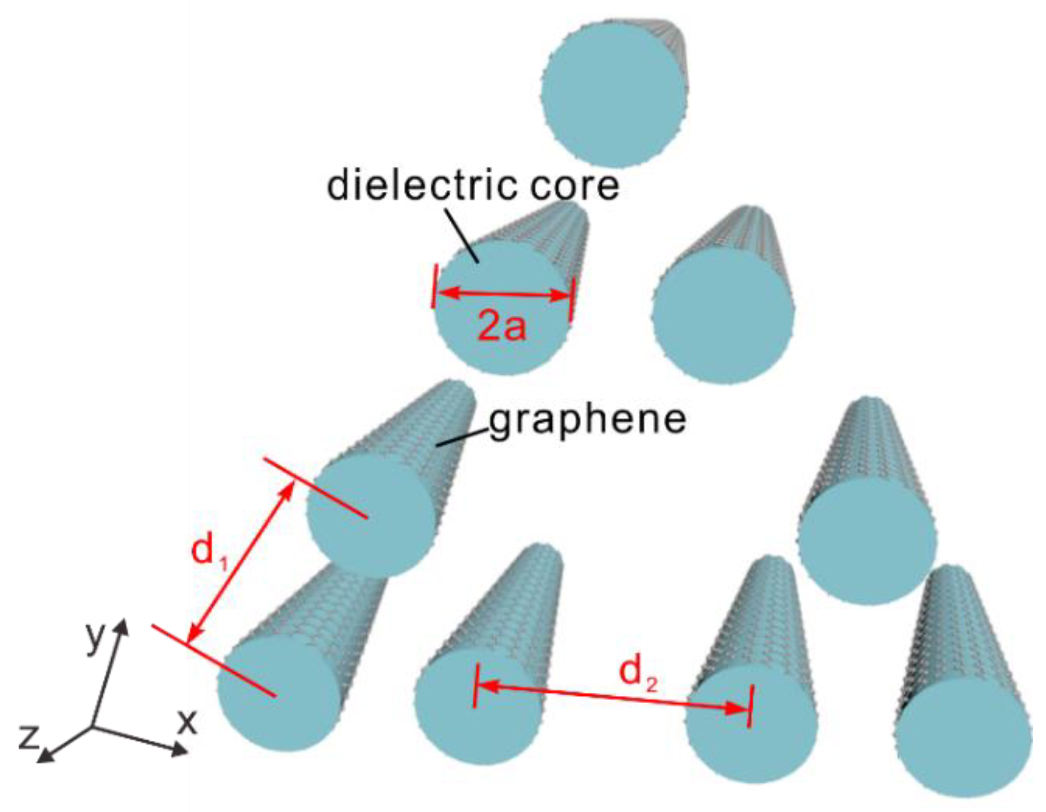
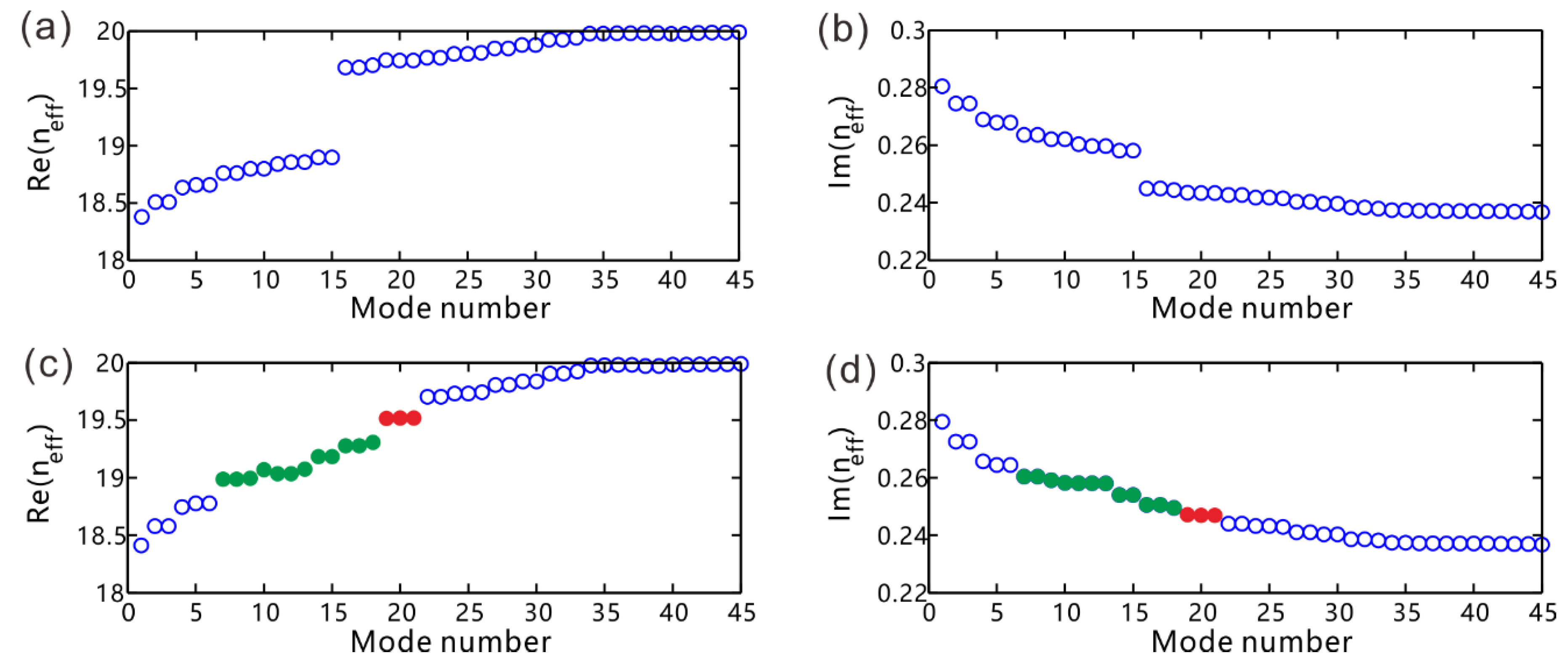
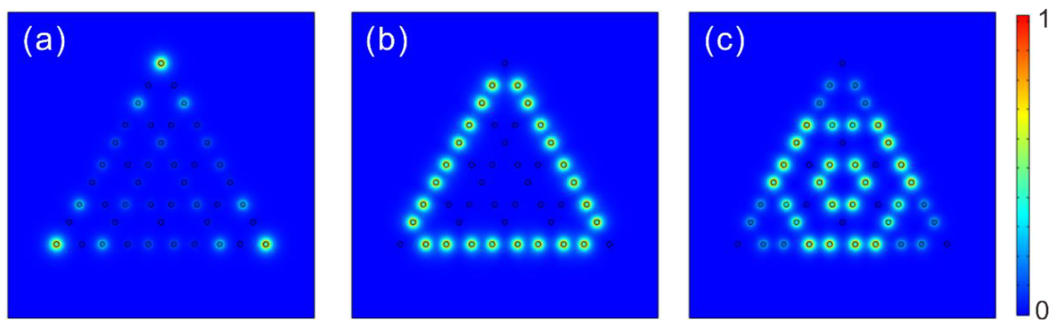
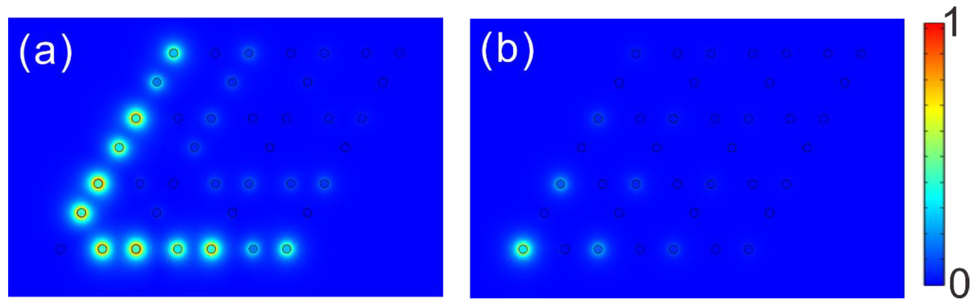
2. Triangle Lattice
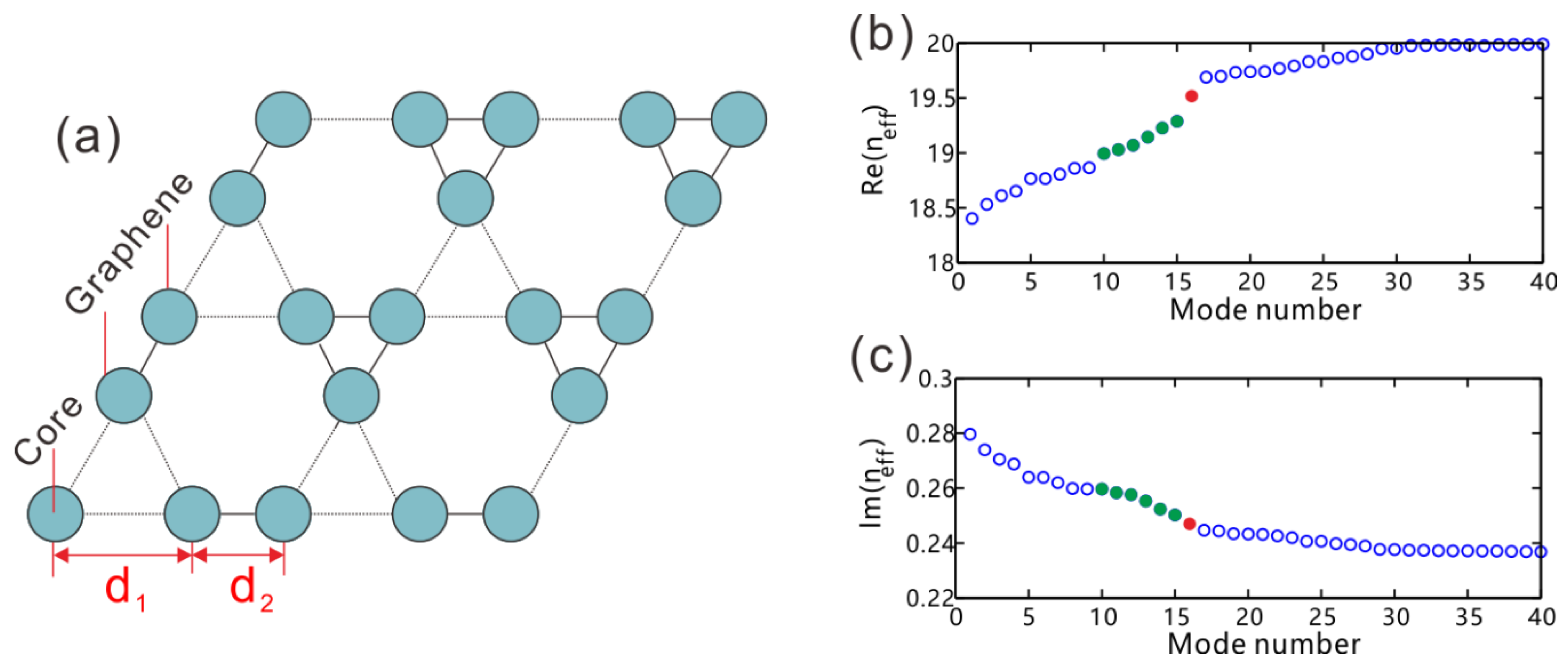
3. Rhombic Lattice
4. Conclusions
Author Contributions
Funding
Conflicts of Interest
References
- Maier, S.A. Plasmonics: Fundamentals and Applications; Springer: Berlin, Germany, 2007. [Google Scholar]
- Ke, S.; Wang, B.; Qin, C.; Long, H.; Wang, K.; Lu, P. Exceptional points and asymmetric mode switching in plasmonic waveguides. J. Lightwave Technol. 2016, 34, 5258–5262. [Google Scholar] [CrossRef] [Green Version]
- Kou, Y.; Förstner, J. Discrete plasmonic solitons in graphene-coated nanowire arrays. Opt. Express 2016, 24, 4714–4721. [Google Scholar] [CrossRef] [PubMed] [Green Version]
- Ke, S.; Wang, B.; Long, H.; Wang, K.; Lu, P. Topological mode switching in a graphene doublet with exceptional points. Opt. Quantum Electron. 2017, 49, 1–12. [Google Scholar] [CrossRef]
- Wang, Z.; Wang, B.; Long, H.; Wang, K.; Lu, P. Surface plasmonic lattice solitons in semi-infinite graphene sheet arrays. J. Lightwave Technol. 2017, 35, 2960–2965. [Google Scholar] [CrossRef] [Green Version]
- Han, X.; Wang, K.; Xing, X.; Wang, M.; Lu, P. Rabi Splitting in a Plasmonic Nanocavity Coupled to a WS2 Monolayer at Room Temperature. ACS Photonics 2018, 5, 3970–3976. [Google Scholar] [CrossRef]
- Bao, Q.; Loh, K.P. Graphene photonics, plasmonics, and broadband optoelectronic devices. ACS Nano 2012, 6, 3677–3694. [Google Scholar] [CrossRef] [PubMed]
- Zhao, D.; Wang, Z.; Long, H.; Wang, K.; Wang, B.; Lu, P. Optical bistability in defective photonic multilayers doped by graphene. Opt. Quantum Electron. 2017, 49, 163. [Google Scholar] [CrossRef]
- Chen, P.Y.; Al, A. Atomically thin surface cloak using graphene monolayers. ACS Nano 2011, 5, 5855–5863. [Google Scholar] [CrossRef]
- Ke, S.; Liu, J.; Liu, Q.; Zhao, D.; Liu, W. Strong absorption near exceptional points in plasmonic waveguide arrays. Opt. Quantum Electron. 2018, 50, 318. [Google Scholar] [CrossRef]
- Zhao, D.; Liu, F.; Meng, P.; Wen, J.; Xu, S.; Li, Z.; Zhong, D. Reflection Enhancement and Giant Lateral Shift in Defective Photonic Crystals with Graphene. Appl. Sci. 2019, 9, 2141. [Google Scholar] [CrossRef] [Green Version]
- Ke, S.; Zhao, D.; Liu, Q.; Liu, W. Adiabatic transfer of surface plasmons in non-Hermitian graphene waveguides. Opt. Quantum Electron. 2018, 50, 393. [Google Scholar] [CrossRef]
- Liu, J.X.; Park, S.; Nowak, D.; Tian, M.C.; Wu, Y.; Long, H.; Wang, K.; Wang, B.; Lu, P. Near-Field Characterization of Graphene Plasmons by Photo-Induced Force Microscopy. Laser Photonics Rev. 2018, 2018, 1800040. [Google Scholar] [CrossRef]
- Zhao, D.; Xu, B.; Guo, H.; Xu, W.; Zhong, D.; Ke, S. Low Threshold Optical Bistability in Aperiodic PT-Symmetric Lattices Composited with Fibonacci Sequence Dielectrics and Graphene. Appl. Sci. 2019, 9, 5125. [Google Scholar] [CrossRef] [Green Version]
- Huang, H.; Ke, S.; Wang, B.; Long, H.; Wang, K.; Lu, P. Numerical study on plasmonic absorption enhancement by a rippled graphene sheet. J. Lightwave Technol. 2017, 35, 320–324. [Google Scholar] [CrossRef]
- Li, J.; Fu, J.; Liao, Q.; Ke, S. Exceptional points in chiral metasurface based on graphene strip arrays. J. Opt. Soc. Am. 2019, 36, 2492–2498. [Google Scholar] [CrossRef]
- Wang, F.; Qin, C.Z.; Wang, B.; Long, H.; Wang, K.; Lu, P.X. Rabi oscillations of plasmonic supermodes in graphene multilayer arrays. IEEE J. Sel. Top. Quant. 2017, 23, 4600105. [Google Scholar] [CrossRef]
- Sanderson, M.; Ang, Y.; Gong, S.; Zhao, T.; Hu, M.; Zhong, R.; Chen, X.; Zhang, P.; Zhang, C.; Liu, S. Optical bistability induced by nonlinear surface plasmon polaritons in graphene in terahertz regime. Appl. Phys. Lett. 2015, 107, 203113. [Google Scholar] [CrossRef] [Green Version]
- Zhao, D.; Ke, S.; Hu, Y.; Wang, B.; Lu, P. Optical bistability of graphene embedded in parity-time-symmetric photonic lattices. JOSA B 2019, 36, 1731–1737. [Google Scholar] [CrossRef]
- Ooi, K.; Ang, S.; Cheng, J.L.; Ang, L.K.; Tan, D.T.H. Electronic scattering of graphene plasmons in the terahertz nonlinear regime. IEEE J. Sel. Top. Quantum Electron. 2017, 23, 5100206. [Google Scholar] [CrossRef]
- Yao, B.; Liu, Y.; Huang, S.-W.; Choi, C.; Xie, Z.; Flores, J.F.; Wu, Y.; Yu, M.; Kwong, D.-L.; Huang, Y.; et al. Broadband gate-tunable terahertz plasmons in graphene heterostructures. Nat. Photonics 2018, 12, 22–28. [Google Scholar] [CrossRef] [Green Version]
- Xu, S.; Zhou, Q.; Zhao, D.; Belic, M.; Zhao, Y. Spatiotemporal solitons in cold Rydberg atomic gases with Bessel optical lattices. Appl. Math. Lett. 2020, 106, 106230. [Google Scholar] [CrossRef]
- Lu, L.; Joannopoulos, J.D.; Soljačić, M. Topological photonics. Nat. Photonics 2014, 8, 821–829. [Google Scholar] [CrossRef] [Green Version]
- Ke, S.; Zhao, D.; Liu, J.; Liu, Q.; Liao, Q.; Wang, B.; Lu, P. Topological bound modes in anti-PT-symmetric optical waveguide arrays. Opt. Express 2019, 27, 13858–13870. [Google Scholar] [CrossRef] [PubMed]
- Liu, F.; Zhao, D.; Cao, H.; Xu, W.; Ke, S. Exceptional Points in Non-Hermitian Photonic Crystals Incorporated with a Defect. Appl. Sci. 2020, 10, 823. [Google Scholar] [CrossRef] [Green Version]
- Deng, H.; Chen, X.; Panoiu, N.C.; Ye, F. Topological surface plasmons in superlattices with changing sign of the average permittivity. Opt. Lett. 2016, 41, 4281–4284. [Google Scholar] [CrossRef] [PubMed]
- Fu, N.; Fu, Z.; Zhang, H.; Liao, Q.; Zhao, D.; Ke, S. Topological bound modes in optical waveguide arrays with alternating positive and negative couplings. Opt. Quantum Electron. 2020, 52, 61. [Google Scholar] [CrossRef]
- Fu, Z.; Fu, N.; Zhang, H.; Wang, Z.; Zhao, D.; Ke, S. Extended SSH Model in Non-Hermitian Waveguides with Alternating Real and Imaginary Couplings. Appl. Sci. 2020, 10, 3425. [Google Scholar] [CrossRef]
- Deng, H.; Chen, Y.; Panoiu, N.C.; Malomed, B.A.; Ye, F. Surface modes in plasmonic Bragg fibers with negative average permittivity. Opt. Express 2018, 26, 2559–2568. [Google Scholar] [CrossRef] [PubMed] [Green Version]
- Cheng, Q.; Pan, Y.; Wang, Q.; Li, T.; Zhu, S. Topologically protected interface mode in plasmonic waveguide arrays. Laser Photonics Rev. 2015, 9, 392–398. [Google Scholar] [CrossRef]
- Pocock, S.R.; Xiao, X.; Huidobro, P.A.; Giannini, V. Topological plasmonic chain with retardation and radiative effects. ACS Photonics 2018, 5, 2271–2279. [Google Scholar] [CrossRef]
- Ling, C.W.; Xiao, M.; Chan, C.T.; Yu, S.F.; Fung, K.H. Topological edge plasmon modes between diatomic chains of plasmonic nanoparticles. Opt. Express 2015, 23, 2021–2031. [Google Scholar] [CrossRef] [PubMed]
- Ge, L.; Wang, L.; Xiao, M.; Wen, W.; Chan, C.T.; Han, D. Topological edge modes in multilayer graphene systems. Opt. Express 2015, 23, 21585–21595. [Google Scholar] [CrossRef] [PubMed]
- Ke, S.; Wang, B.; Long, H.; Wang, K.; Lu, P. Topological edge modes in non-Hermitian plasmonic waveguide arrays. Opt. Express 2017, 25, 11132–11143. [Google Scholar] [CrossRef] [PubMed]
- Meng, P.; Zhao, D.; Zhong, D.; Liu, W. Topological plasmonic modes in graphene-coated nanowire arrays. Opt. Quantum Electron. 2019, 51, 156. [Google Scholar] [CrossRef]
- Wang, F.; Ke, S.; Qin, C.; Wang, B.; Long, H.; Wang, K.; Lu, P. Topological interface modes in graphene multilayer arrays. Opt. Laser Technol. 2018, 103, 272–278. [Google Scholar] [CrossRef]
- Ge, L.; Liu, L.; Xiao, M.; Du, G.; Shi, L.; Han, D.; Chan, C.T.; Zi, J. Topological phase transition and interface states in hybrid plasmonic-photonic systems. J. Opt. 2017, 19, 1–5. [Google Scholar] [CrossRef] [Green Version]
- Xu, C.; Zhang, P.; Zhao, D.; Guo, H.; Huang, M.; Ke, S. Plasmonic Jackiw-Rebbi Modes in Graphene Waveguide Arrays. Appl. Sci. 2019, 19, 4152. [Google Scholar] [CrossRef] [Green Version]
- Jin, D.; Christensen, T.; Soljačić, M.; Fang, N.X.; Lu, L.; Zhang, X. Infrared Topological Plasmons in Graphene. Phys. Rev. Lett. 2017, 118, 245301. [Google Scholar] [CrossRef] [Green Version]
- Benalcazar, W.A.; Bernevig, B.A.; Hughes, T.L. Quantized electric multipole insulators. Science 2017, 357, 61–66. [Google Scholar] [CrossRef] [PubMed] [Green Version]
- Imhof, S.; Berger, C.; Bayer, F.; Brehm, J.W.; Molenkamp, L.; Kiessling, T.; Schindler, F.; Lee, C.; Greiter, M.; Neupert, T.; et al. Topolectrical-circuit realization of topological corner modes. Nat. Phys. 2018, 14, 925–929. [Google Scholar] [CrossRef]
- Serra-Garcia, M.; Peri, V.; Süsstrunk, R.; Bilal, O.R.; Larsen, T.; Guillermo, L.; Huber, S.D. Observation of a phononic quadrupole topological insulator. Nature 2018, 555, 342–345. [Google Scholar] [CrossRef] [PubMed]
- Peterson, C.W.; Benalcazar, W.A.; Hughes, T.L.; Bahl, G. A quantized microwave quadrupole insulator with topologically protected corner states. Nature 2018, 555, 346–350. [Google Scholar] [CrossRef] [PubMed]
- Xue, H.; Yang, Y.; Gao, F.; Chong, Y.; Zhang, B. Acoustic higher-order topological insulator on a kagome lattice. Nat. Mater. 2019, 18, 108–112. [Google Scholar] [CrossRef] [PubMed] [Green Version]
- Chen, X.-D.; Deng, W.-M.; Shi, F.-L.; Zhao, F.-L.; Chen, M.; Dong, J.-W. Direct observation of corner states in second-order topological photonic crystal slabs. Phys. Rev. Lett. 2019, 122, 233902. [Google Scholar] [CrossRef] [PubMed] [Green Version]
- Chen, Y.; Lin, Z.; Chen, H.; Jiang, J. Plasmon-polaritonic quadrupole topological insulators. Phys. Rev. 2020, 101, 041109. [Google Scholar] [CrossRef] [Green Version]
- Ota, Y.; Liu, F.; Katsumi, R.; Watanabe, K.; Wakabayashi, K.; Arakawa, Y.; Iwamoto, S. Photonic crystal nanocavity based on a topological corner state. Optica 2019, 6, 786–789. [Google Scholar] [CrossRef]
- Mittal, S.; Orre, V.; Zhu, G.; Gorlach, M.A.; Poddubny, A.; Hafezi, M. Photonic quadrupole topological phases. Nat. Photonics 2019, 13, 692–696. [Google Scholar] [CrossRef] [Green Version]
- Xu, Y.; Xue, R.; Wan, S. Topological corner states on kagome lattice based chiral higher-order topological insulator. arXiv 2017, arXiv:1711.09202. [Google Scholar]
- Ezawa, M. Higher-Order Topological Insulators and Semimetals on the Breathing Kagome and Pyrochlore Lattices. Phys. Rev. Lett. 2018, 120, 026801. [Google Scholar] [CrossRef] [PubMed] [Green Version]
- Hassan, E.; Ashraf Flore, K.; Kunst, A.M.; Andler, G.; Emil, J.; Bourennane, B.; Bourennane, M. Corner states of light in photonic waveguides. Nat. Photonics 2019, 13, 697–700. [Google Scholar] [CrossRef] [Green Version]
- Atanasov, V.; Saxena, A. Tuning the electronic properties of corrugated graphene: Confinement, curvature, and band-gap opening. Phys. Rev. 2010, 81, 205409. [Google Scholar] [CrossRef] [Green Version]
- Atanasov, V.; Saxena, A. Electronic properties of corrugated graphene: The Heisenberg principle and wormhole geometry in the solid state. J. Phys. Condens. Matter 2011, 23, 175301. [Google Scholar] [CrossRef] [PubMed] [Green Version]


© 2020 by the authors. Licensee MDPI, Basel, Switzerland. This article is an open access article distributed under the terms and conditions of the Creative Commons Attribution (CC BY) license (http://creativecommons.org/licenses/by/4.0/).
Share and Cite
Liu, N.; Ding, C.; Liao, Q.; Ke, S. Topological Corner Modes in Graphene-Coated Nanowire Waveguide. Appl. Sci. 2020, 10, 4027. https://doi.org/10.3390/app10114027
Liu N, Ding C, Liao Q, Ke S. Topological Corner Modes in Graphene-Coated Nanowire Waveguide. Applied Sciences. 2020; 10(11):4027. https://doi.org/10.3390/app10114027
Chicago/Turabian StyleLiu, Ningliang, Chizhu Ding, Qing Liao, and Shaolin Ke. 2020. "Topological Corner Modes in Graphene-Coated Nanowire Waveguide" Applied Sciences 10, no. 11: 4027. https://doi.org/10.3390/app10114027