Article

A Uniform Eddy Current Probe with a Double-Excitation Coil for Flaw Detection on Aluminium Plates

by
Ageng Sadnowo Repelianto
1,2,*,
Naoya Kasai
1,*,
Kouichi Sekino
3 and
Masaki Matsunaga
1
1
Department of Risk Management and Environmental Sciences, Graduate School of Environment and Information Sciences, Yokohama National University, Yokohama 240-8501, Japan
2
Department of Engineering, Lampung University, Lampung 35145, Indonesia
3
Department of Mechanical and Materials Engineering, Kanagawa Institute of Industrial Science and Technology, Yokohama 243-0435, Japan
*
Authors to whom correspondence should be addressed.
Metals 2019, 9(10), 1116; https://doi.org/10.3390/met9101116
Submission received: 6 September 2019 / Revised: 8 October 2019 / Accepted: 15 October 2019 / Published: 19 October 2019

Abstract

:
In this present study, a new uniform eddy current (UEC) probe with a double-excitation coil and pancake orientation is proposed. It is confirmed that the probe generates a strong magnetic field induction that increases the intensity of uniform eddy currents; moreover, it is found to be more efficient in power consumption for excitation using a finite element simulation. Experiments are performed to detect different flaw lengths and depths on an aluminium plate. The flaw signal detected by the probe indicates a high signal-to-noise ratio and increases as a function of flaw depth. The quantitative evaluation of flaws with the proposed UEC probe is achieved based on experimental results.

Graphical Abstract

1. Introduction

Eddy current testing is widely used as a non-destructive testing technique in the industry to evaluate the size of flaws in structural components [1,2,3]. To date, researchers in both academia and industry continue to investigate and develop new eddy current probes to achieve high signal-to-noise (S/N) ratios of flaw signals [4,5].
Based on their configurations, eddy current probes are generally classified into two types. One is the combined transmit-receive probe equipped with a single coil that functions as an excitation coil and a detection coil. The concept of this single coil is based on the principle that a change in impedance occurs when discontinuities disrupt the eddy current distribution in the test piece [2,6].
Another type of eddy current probe is the separate transmit-receive (STR) probe that has two distinct coils, one for excitation and another for detection. A unique model of the STR probe is the uniform eddy current (UEC) probe. This probe has been developed to resist the effects of lift-off caused by the uneven surface of test materials, such as those found in weld zones [7,8,9,10,11,12,13,14]. UEC probes are for detecting flaws on the surface of the test piece with high frequency of excitation current and are specially designed to have resistance to lift-off variation in the measurement [1,7,8].
The nature of the UEC probe results from the self-differential properties possessed by its detector coil. The electromotive forces (emfs) generated on opposite parts of a detection coil are the same but have opposite polarities; accordingly, they cancel out each other. As a result, the output voltage, VO of the coil is zero; this nature is called self-nulling [7,11,13,15]. Because the UEC probe reduces the effect of lift-off on the measurement signal, the signal can be regarded as a reliable sizing indicator of the flaw [16,17]. However, because the excitation coil of the UEC probe is tangentially oriented, its signal is relatively small. In this configuration, not all parts of the detection coil contribute to induce the signal; only parts that are close and parallel to the test piece are actively involved in this regard. To overcome these relatively small signals, several trials using excitation currents with high frequencies and amplifier circuits have been conducted [11,12,18,19].
In the present study, a new demand for eddy current testing is for portable instruments able to detect smaller and buried flaws, using a lower amplitude of excitation currents. Thus, the operational time of the probe can be longer. In this study a probe with double excitation coils was used with a giant magnetoresistance sensor [20]. The configuration and shape of excitation and detection coils were designed to enhance the S/N ratio and power supply efficiency during measurement [21,22].
The proposed UEC probe consists of a pair of rectangular excitation coils and a circular detection coil; all coils are in a pancake orientation. The authors named the device the ‘butterfly probe’. The flaw detection principle involved in the butterfly probe is analysed with a finite element simulation. Its ability to detect flaws on the aluminium plate surface is discussed based on experimental results.

2. Materials and Methods

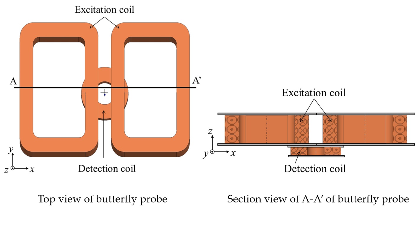
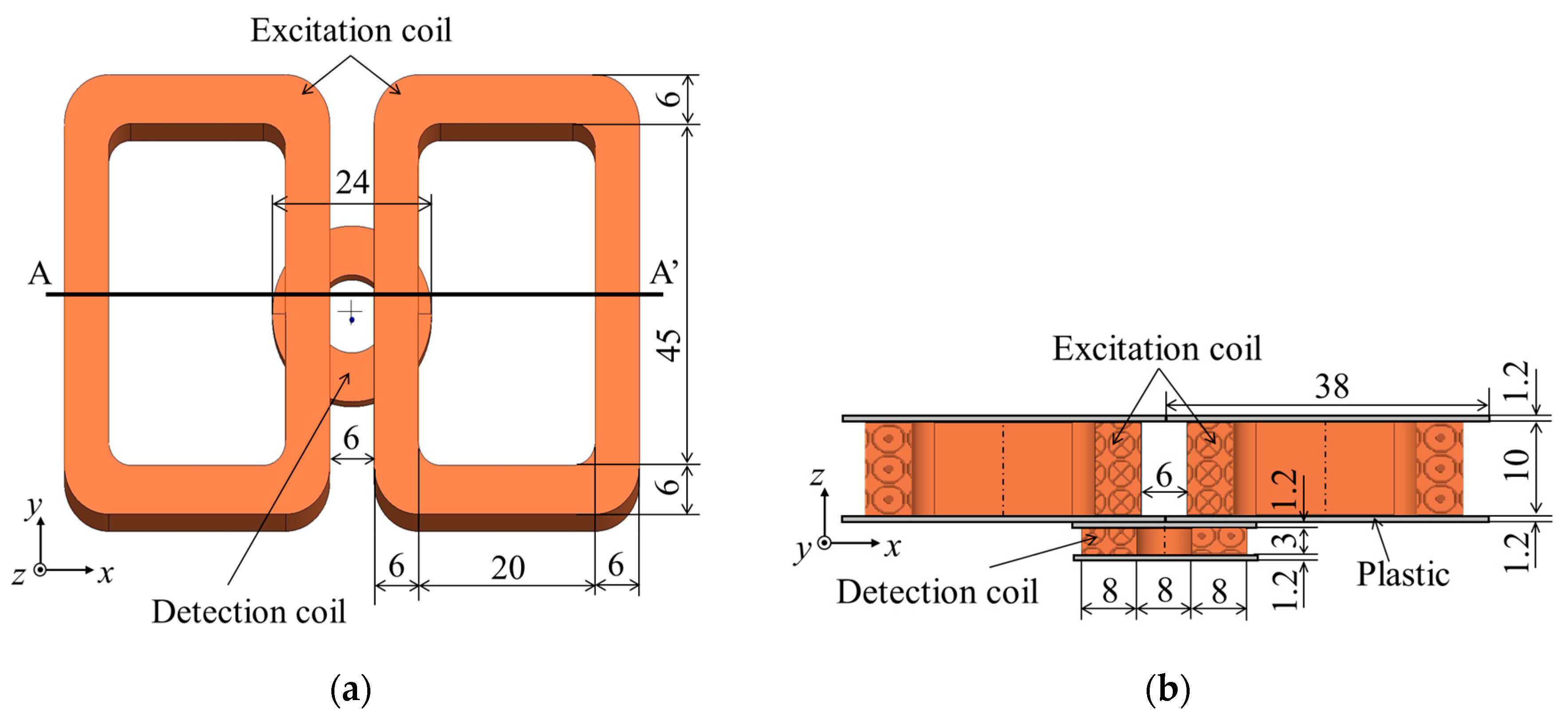
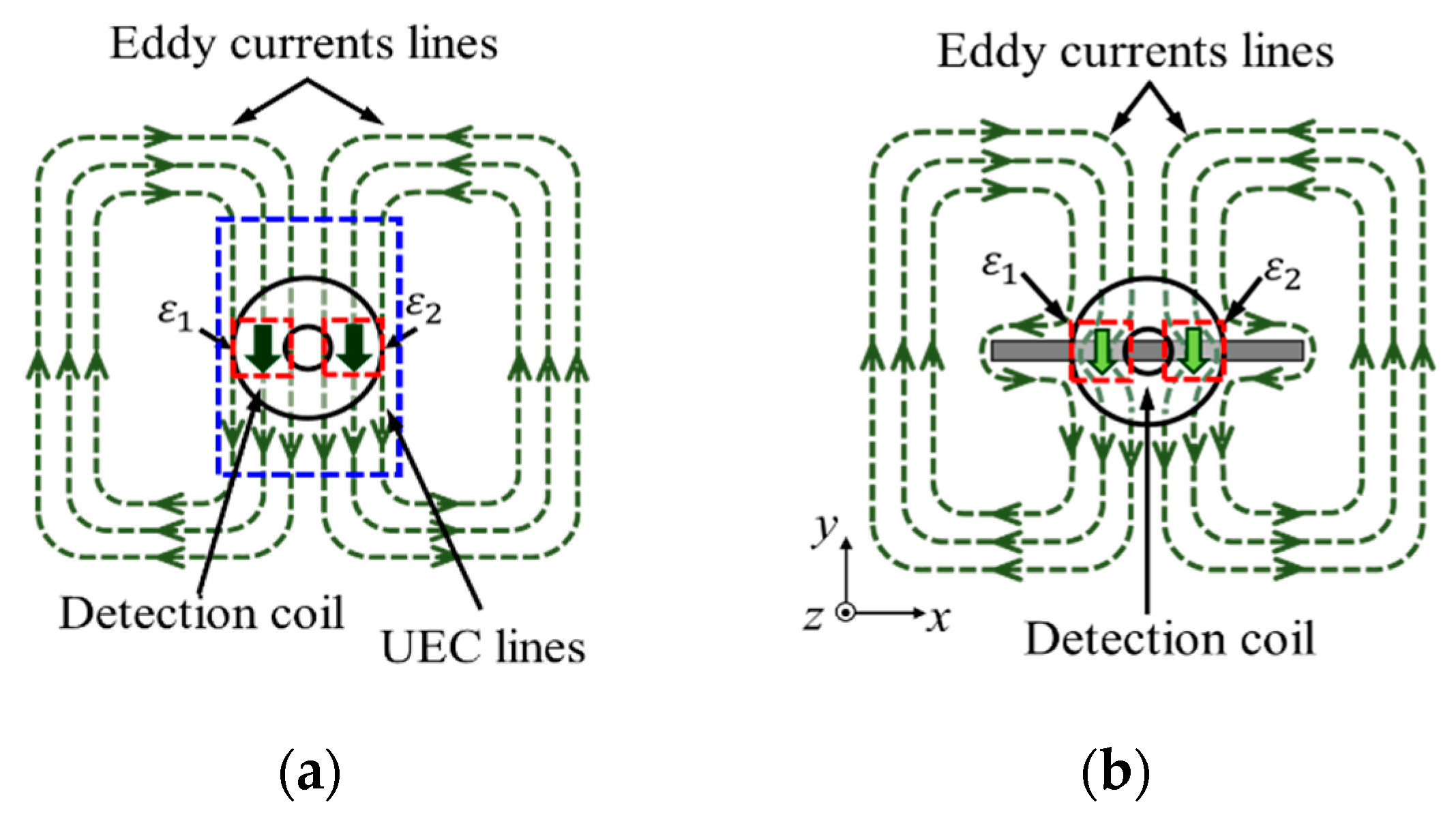
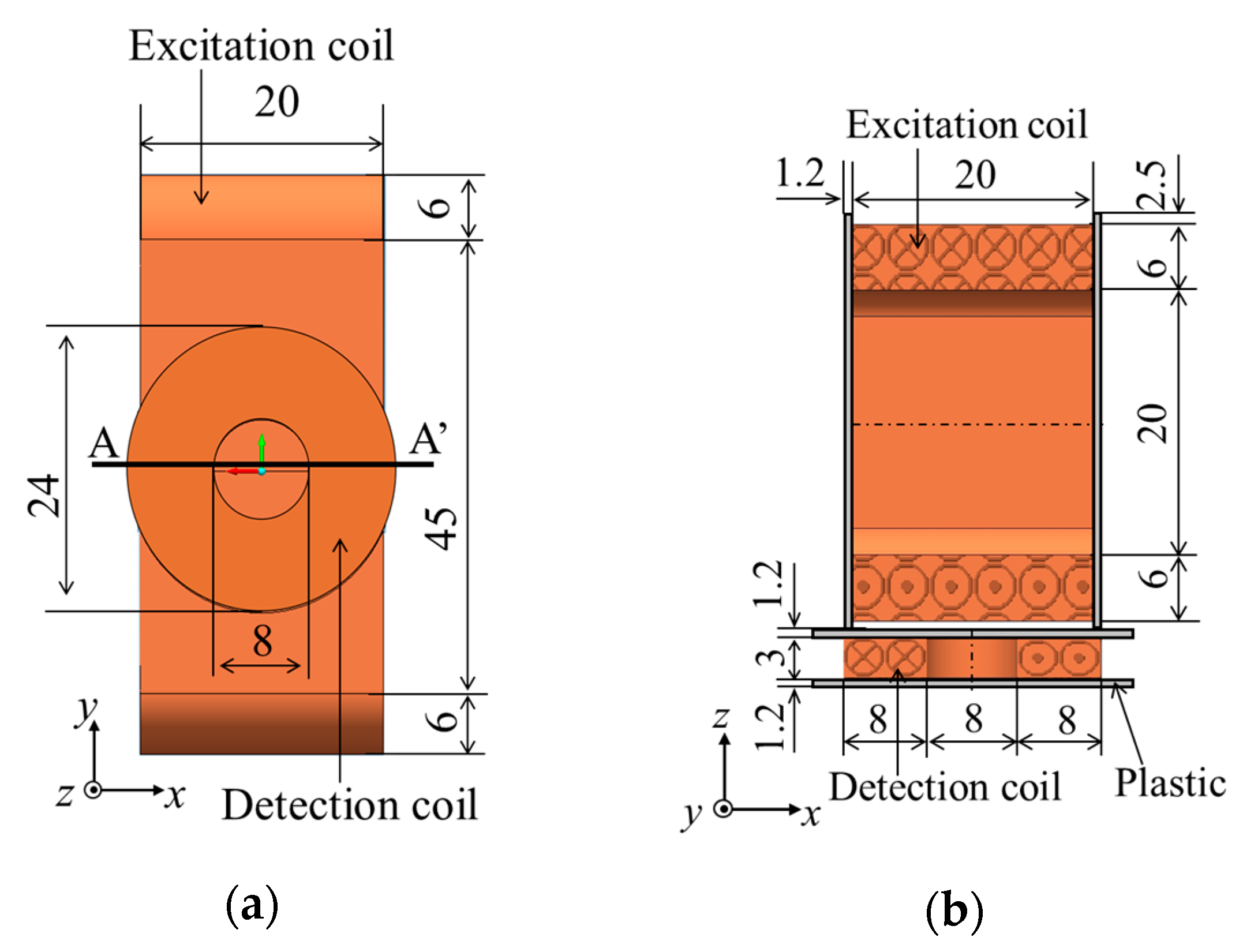
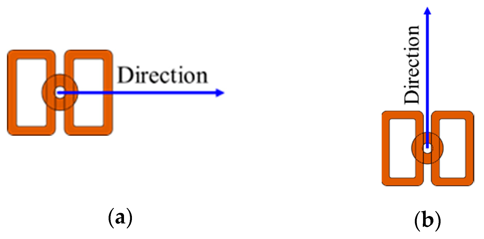
2.1. Butterfly Probe Design

To improve the detection capability of an eddy current probe, an essential factor is increasing the intensity of eddy currents generated by the probe. Accordingly, the butterfly probe has a pair of excitation coils with the same dimensions but wound in opposite directions; specifications are as shown in Figure 1. Each excitation coil generates an eddy current that is opposite in circulation to the coil’s winding direction. The circular detection coil is installed at the bottom and centre of the coils.
On the area with a blue dotted line shown in Figure 2, the eddy currents of the two coils merge and form uniform eddy currents with an intensity that is practically twice that of the eddy current from one coil.
There are two conditions in the butterfly probe: balanced and unbalanced conditions. These conditions are determined by the response of the interaction zone of the detection coil against the uniform eddy current, as shown by the red dotted line in Figure 2.
Under the balanced condition, emfs ε1 and ε2 of the detection coil are of the same amplitude, but opposite in polarities; as a result, they cancel out each other. Consequently, the detection coil output is zero; a nature called self-nulling. The output is also zero when the probe is positioned in the middle of a flaw, as shown in Figure 2b; this is because the eddy currents have the same disturbance at two sides of the detection coil.
The unbalanced condition shown in Figure 3 is divided into two models. The model in which the edge of a flaw is located under the detection coil is shown in Figure 3a. Because the disturbance caused by the flaw caused ε1 and ε2 of the detection coil to have unequal amplitudes, a generating output results.
The model in which a flaw is located a short distance away from the detection coil and disrupts the circulation eddy current is shown in Figure 3b. The flaw causes ε1 and ε2 of the detection coil to have unequal amplitudes; this also results in a generating output.
As mentioned above, the middle of the probe is the most sensitive area for detecting flaws.
To achieve the best accuracy, an important factor for the butterfly probe is that the specifications of the two excitation coils should be the same. Moreover, the detection coil must be installed in such a position where self-nulling occurs.

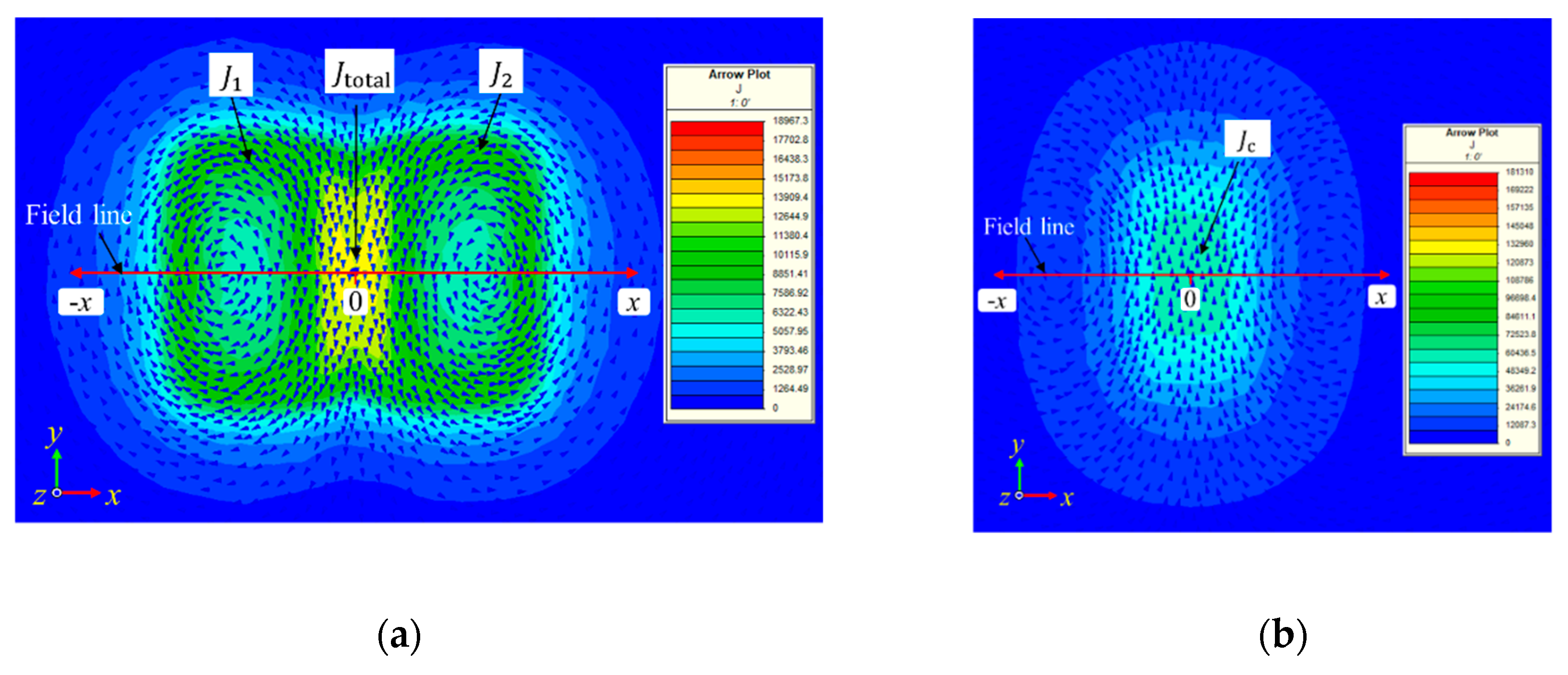
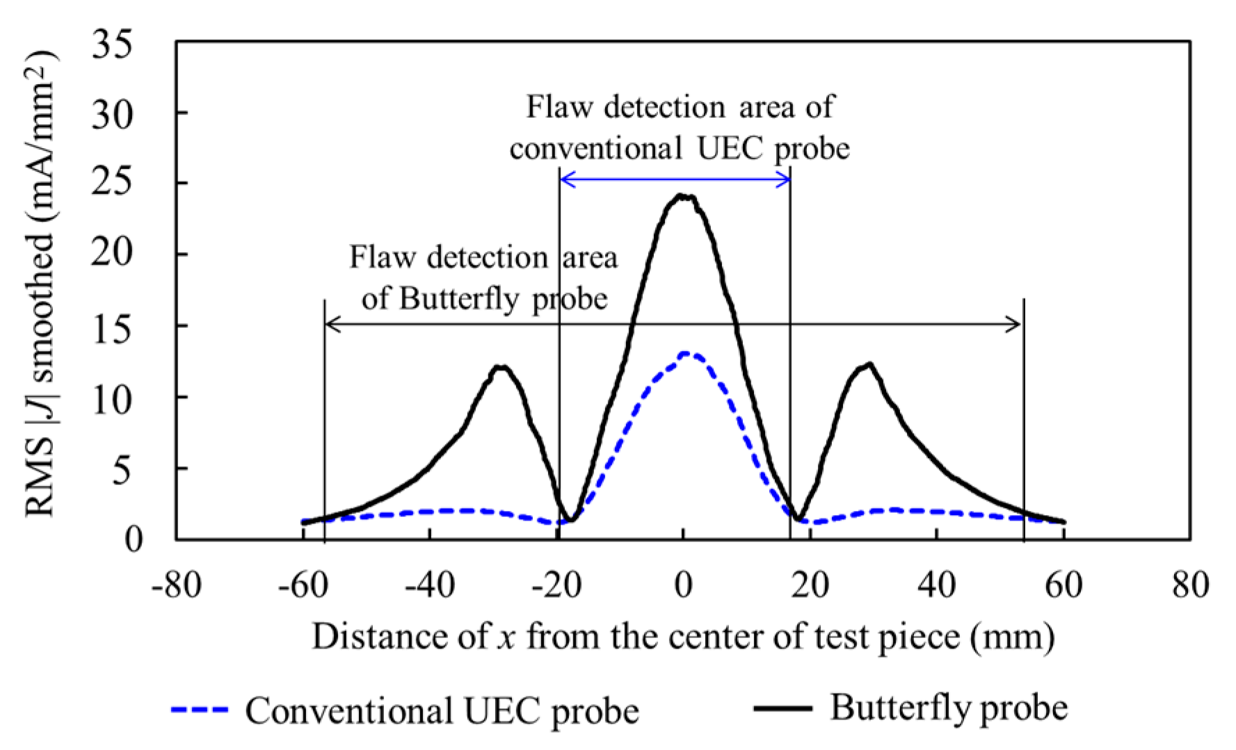
2.2. Numerical Calculations

To observe the distribution of eddy currents in the test pieces using the conventional UEC and butterfly probes, a time-harmonic analysis was implemented by employing finite element analysis software (Magnet 7 version 7.4.1, Mentor Graphics Corporation, Wilsonville, OR, USA). The sizes of the probes used in the analysis were the same as those shown in Figure 1; Figure 4. An aluminium plate, 315 mm in length, 315 mm in width, and 10 mm in thickness, was used as a test piece. The electromagnetic parameters used in the analysis are listed in Table 1. The excitation frequency and current for both probes are 10 kHz and 6 mA, respectively.
The analytical results are shown in Figure 5. In Figure 5a, the amplitudes of the eddy currents of J1 and J2 generated by each excitation coil of the butterfly probe are practically the same. Moreover, the induction, Jtotal, which is a UEC produced by both coils, is twice as large as J1 (or J2).
Meanwhile, in the conventional UEC probe shown in Figure 4, the eddy current (Jc) is smaller, as shown in Figure 5b, although the number of coil turns is the same as that in both excitation coils of the butterfly probe. The reason for this difference is that only the bottom part of the excitation coil of the conventional UEC probe mainly contributes to induction of the eddy current.
The amplitudes of eddy currents are measured along the x-direction (red line) shown in Figure 5; results are shown in Figure 6.
The eddy current density that is generated using the conventional UEC probe indicates only one amplitude peak. Meanwhile, the eddy current density generated using the butterfly probe indicates three peaks. The largest peak, which is located at the middle, is approximately 1.9 times greater than the other peaks. The largest peak of the butterfly probe is 1.8 times larger than that of the conventional UEC probe. Furthermore, because the eddy current distribution is wider, the detection area of the butterfly probe is three times wider than that of the conventional UEC probe; this is true although the signal is small on the area far from the center of the butterfly probe.

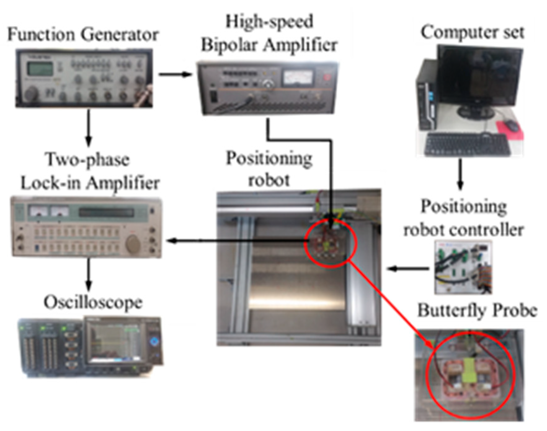
2.3. Experimental Setup

Aluminium plate 5052 is used as the test plate, as shown in Figure 7. On the surface, there are four artificial cracks whose sizes are listed in Table 2; their positions are shown in Figure 7.
The experimental setup is shown in Figure 8. The probes, including the excitation and detection coils, are arranged as shown in Figure 1. The specifications of the coils are summarised in Table 3. The excitation current of the sine wave with a 10-kHz cycle for the probe is generated using a function generator (WAVETEK Model 19, Wavetek Co., San Diego, CA., USA) and amplified to 6 mA with a high-speed bipolar amplifier (NF HAS 4012, NF Co., Yokohama, Japan).
The signal from the detection coil is processed with a two-phase lock-in amplifier (NF 5601B, NF Co., Yokohama, Japan) and stored in a digital oscilloscope (GL7000, Graphtec Co., Yokohama, Japan) with a 4-Hz data sampling capacity. To move the butterfly probe over the scanning surface of the test piece, a computer-controlled positioning robot module (X-SEL controller, IAI Co., Shizuoka, Japan) is used; the robot speed is 10 mm/s. The scanning interval is 2.5 mm in the x-direction and 2.5 mm in the y-direction. The clearance between the probe and aluminium plate surface is approximately 2 mm.
The butterfly probe has two scanning directions, as shown in Figure 9. Scanning 1 is perpendicular to the sensitive axis of the excitation coil; scanning 2 is parallel to the sensitive axis of this coil.

3. Experimental Results and Discussion

The scanning area and paths on the test piece is shown in Figure 10. In scanning 1, the butterfly probe moves in the x-direction and shifts in the y-direction, and is repeated until the scanning covers all the flaws. Scanning 2 is the opposite of scanning 1. The probe moves in the y-direction and shifts in the x-direction.

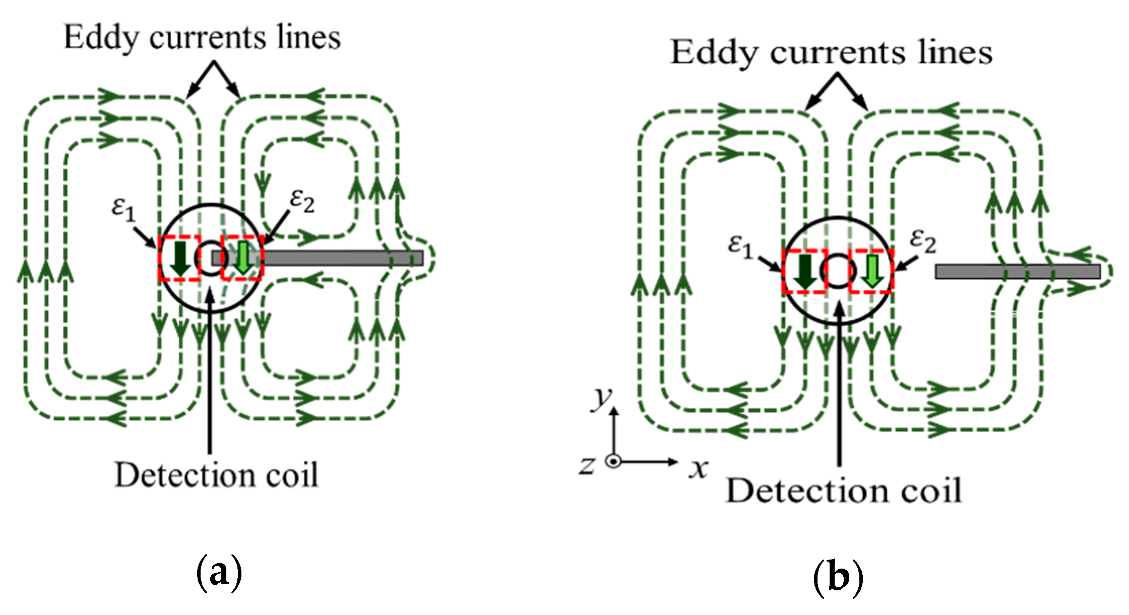
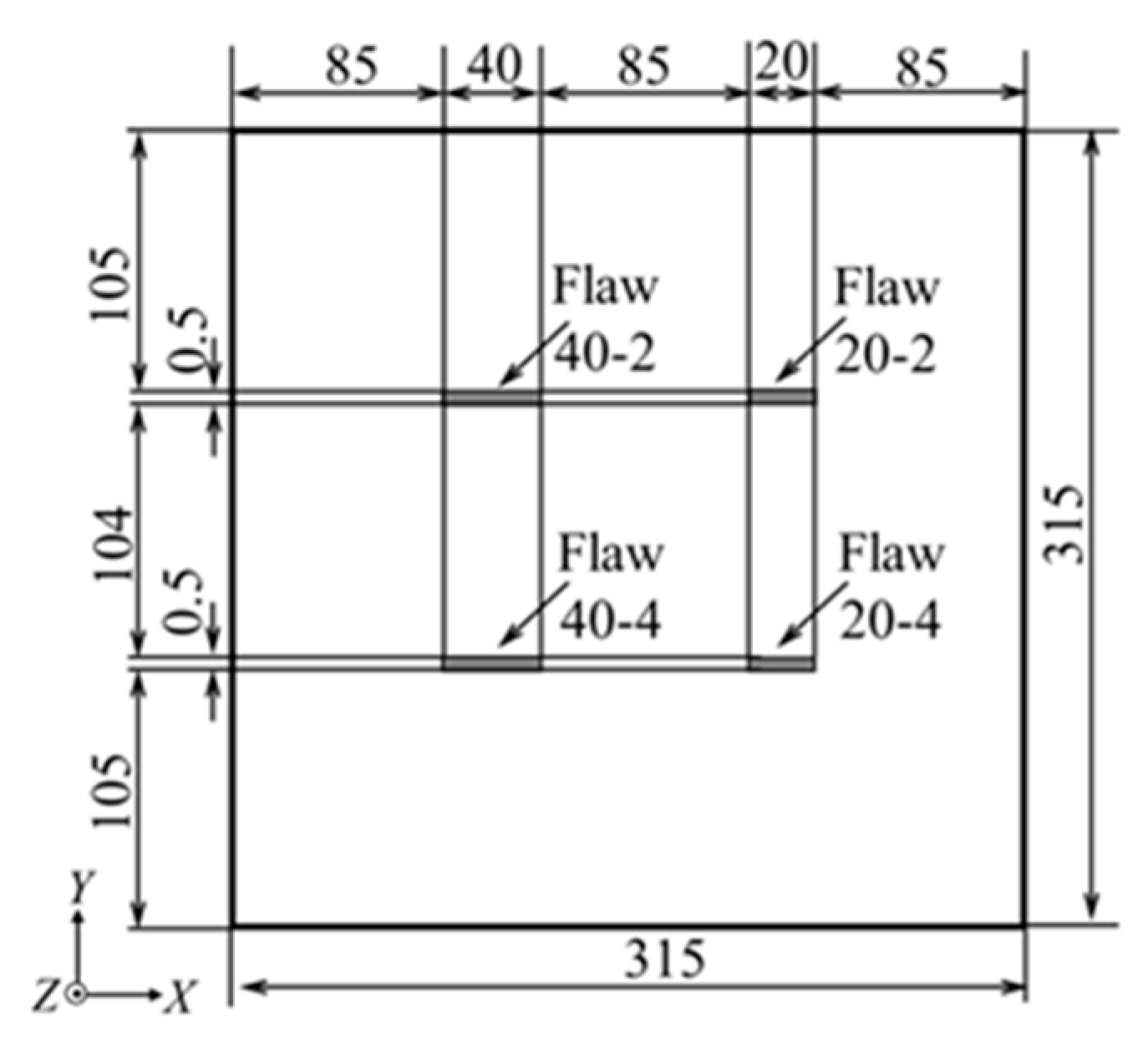
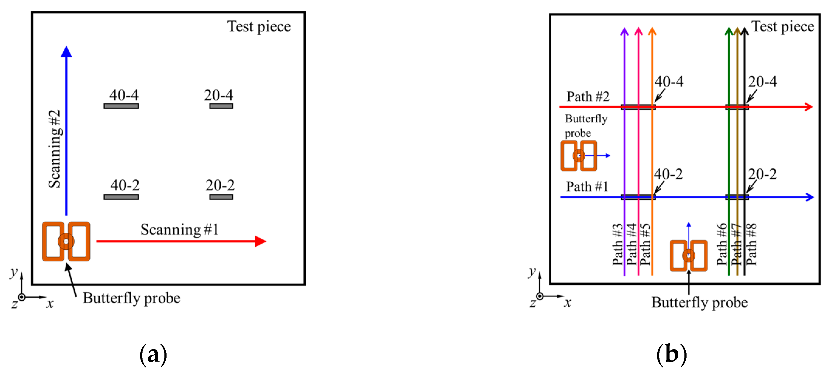
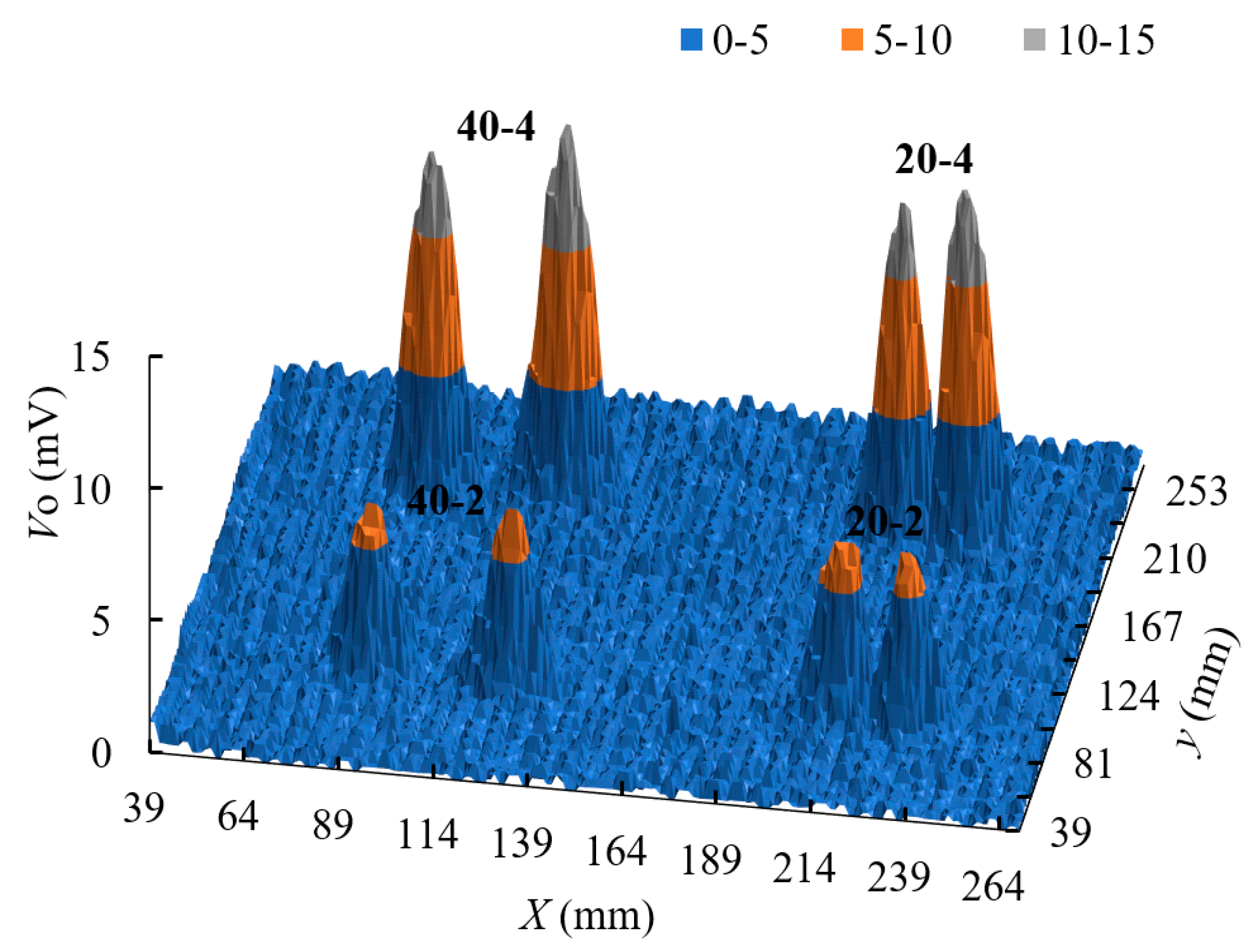
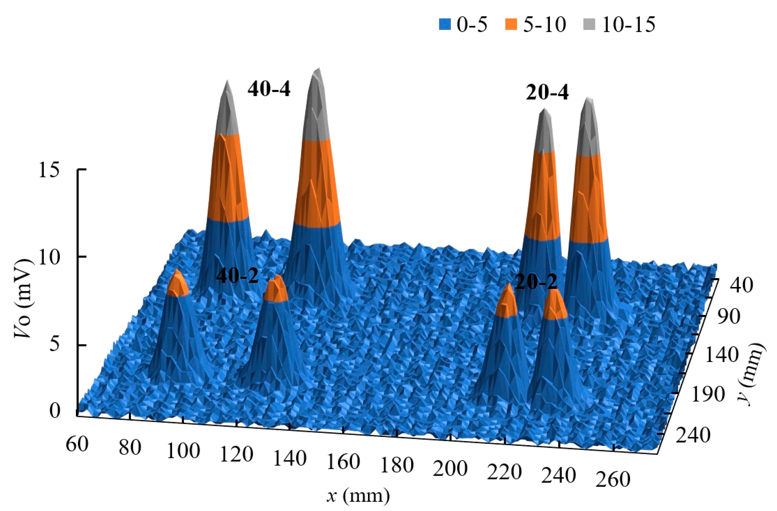
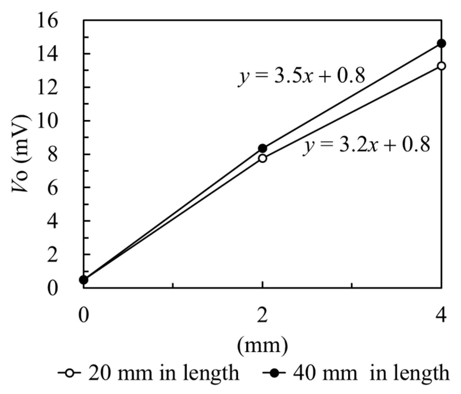
3.1. Measurement of Flaws in Scanning 1 and Scanning 2

Measurement results are shown in Figure 11 for scanning 1, and Figure 12 for scanning 2. In Figure 2; Figure 3, it can be observed that the flaws can be clearly detected, and the signal has a pair of peaks representing the length of the flaw. When the detection coil passes over the middle of the flaw length, the detection coil does not generate any significant signal because of the balanced condition of the coil, as shown in Figure 2b.
The experiments show that the butterfly probe generates better flaw signals in larger regions. Although the flaw is not under the detection coil when the excitation coil covers the flaw, the butterfly probe still produces signals, as shown in Figure 3b. The largest signal is generated when the flaw is under the detection coil.

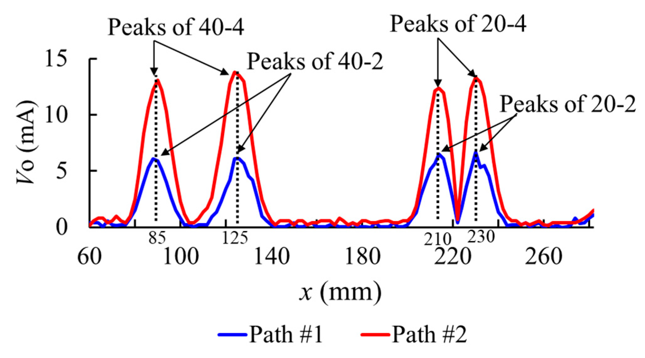
3.2. Measurement Results along Paths #1 and #2 with Scanning 1

The butterfly probe moves along paths #1 and #2, as shown in Figure 10; measurement results are shown in Figure 13.
Figure 13 shows a quantitative measurement of flaws. The length of the flaw is given by the distance between the two signal peaks, whereas the signal amplitude indicates the flaw depth.
Hence, in flaws with the same lengths, such as 40–4 and 40–2, or 20–4 and 20–2, the distance between two peaks of measured signals corresponds to flaw length. The peaks of the signal for 40-4 are twice that of the signal for 40–2. Because the tendencies of the signals for 20–4 and 20–2 are the same, the flaw depth can be quantitatively evaluated based on the amplitude of measured signals.

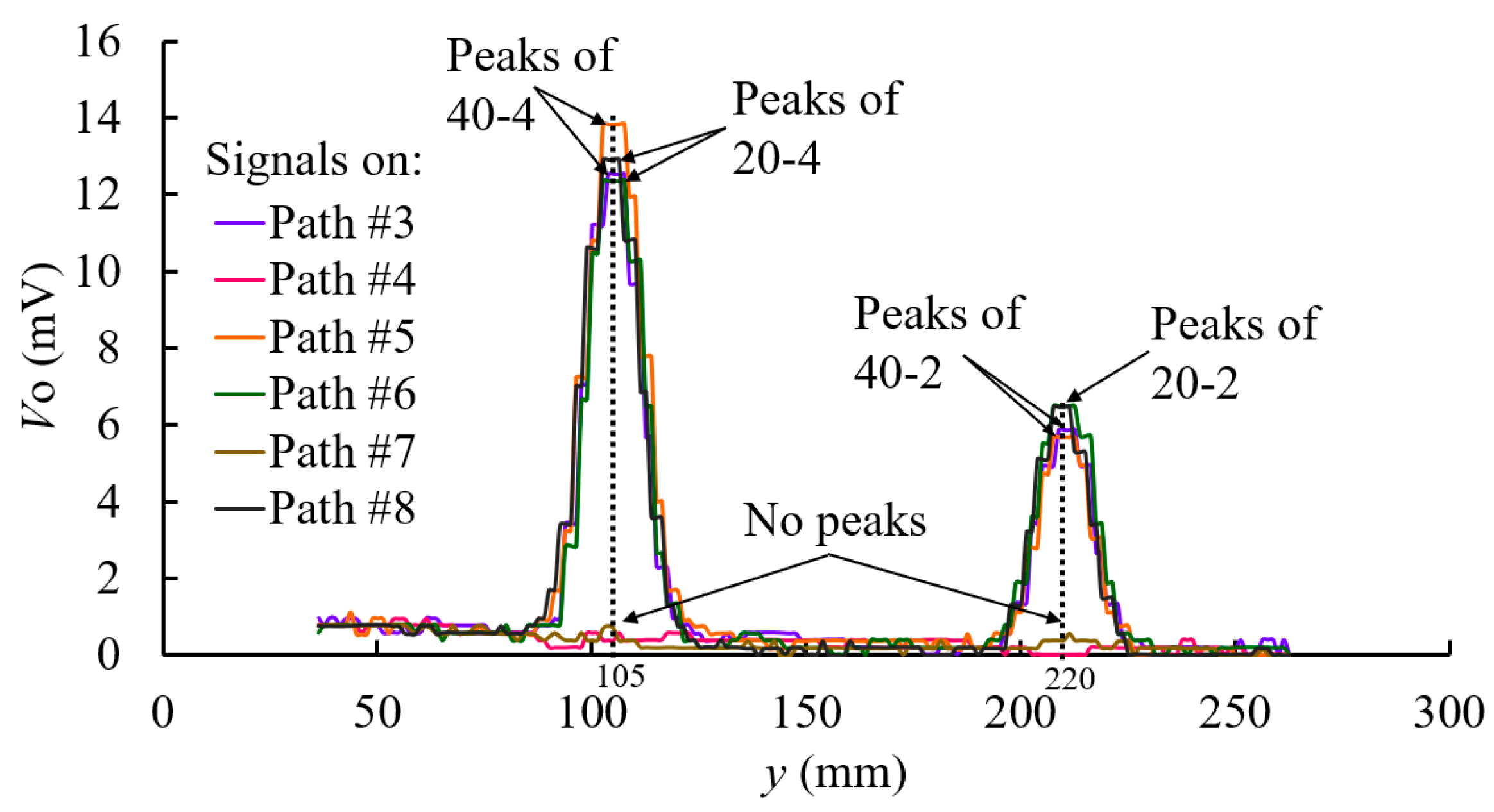
3.3. Measurement Results along Paths #3–#8 with Scanning 2

To describe the detection ability of the butterfly probe, the probe is moved along paths #3–#8 with scanning 2; results are shown in Figure 14.
The signals through paths #4 and #7 do not indicate any peaks. As the detection coil passes through the middle of the length of the flaw, it does not generate any significant signal because of this coil’s balanced condition, as shown in Figure 2b.
Furthermore, the signals along paths #3, #5, #6 and #8 indicate two different peaks for two flaws. The first peak is approximately 12 mV, and the second is approximately 6 mV, which is half of the first signal amplitude.
The results indicate that the probe can accurately evaluate flaws. The butterfly probe is also useful in evaluating flaw depth with scanning 2, which is for the angle of flaw; scanning 2 differs from scanning 1 by 90°.
The effect of flaw length and depth on signal amplitude is shown in Figure 15. The amplitude is approximately the same as the flaw depth. This indicates that the length of the flaw does not have a significant influence on evaluating flaw depth.
From the results of scanning 1 and 2, there was no significant difference between the detection signals. Both results have two amplitude peaks for each flaw that was relatively similar. These results show that the probe can clearly detect the flaws.
As for the effect of the lift-off on measurement, the amplitude of the signals on lift-off from 0 mm to 1 mm decreased from 14.6 mV to 12.5 mV for the flaw with the length of 40 mm and depth of 4 mm. The amplitude of the signals on lift-off from 0 mm to 1 mm decreased from 13.3 mV to 11.1 mV for the flaw with the length of 20 mm and depth of 4 mm. By using signals of lift-off value of 1 mm, the flaw depths were evaluated to 3.3 mm and 3.2 mm for the flaw with the length of 40 mm and 20 mm, respectively, which were an approximately 20% evaluation error.
Besides, a disadvantage of the developed probe is that it cannot detect flaws whose direction of the length is parallel to the uniform eddy current generated from the probe. Therefore, to detect flaws with unknown orientation, scanning in the field test must be carried out twice, in an orthogonal direction to each other.

4. Conclusions

In the present study, a new uniform eddy current probe with double-excitation coils, named the butterfly probe, is proposed.
In the finite element simulation analysis, the maximum eddy current density that is generated using the butterfly probe is 1.8 times larger than that using the conventional UEC probe. The butterfly probe can clearly detect a flaw; the signals have a pair of peaks that correspond to the flaw length. When the detection coil passes through the middle of the flaw length, the detection coil does not generate significant signals because of the balanced condition of the detection coil. Meanwhile, the largest signal is generated when the edge of the flaw is under the detection coil.
In addition, the butterfly probe generates better flaw signals with larger regions and is able to evaluate flaw depth with scanning 2. Scanning 2 is also used for detecting the angle of the flaw and differs from scanning 1 by 90°. Because the flaw length evaluation does not significantly affect flaw depth measurement results, the butterfly probe may be regarded as superior in terms of its reliable flaw depth evaluation.

Author Contributions

Conceptualization, A.S.R. and N.K.; methodology, A.S.R.; software, N.K.; validation, A.S.R. and N.K.; formal analysis, A.S.R., K.S. and N.K.; investigation, A.S.R., K.S., and M.M.; resources, K.S.; data curation, A.S.R. and M.M.; writing—original draft preparation, A.S.R.; writing—review and editing, A.S.R. and N.K.; visualization, A.S.R. and M.M.; supervision, N.K.; project administration, A.S.R.; funding acquisition, N.K.

Funding

This research was founded by the Yokohama National University, The Japan Welding Engineering Society and the Scholarships of Excellence for Indonesian Lecturers (BUDI)–Indonesia Endowment Fund for Education (LPDP) of the Research, Technology and Higher Learning Ministry of Indonesia.

Acknowledgments

The authors gratefully acknowledge the financial support from Yokohama National University, the Japan Welding Engineering Society, the Indonesian Directorate General for Higher Education and Ministry of Finance, and the Republic of Indonesia through Indonesia Endowment Fund for Education (BUDI–LPDP) Scholarship.

Conflicts of Interest

The authors declare no conflict of interest.

References

  1. Sophian, A.; Tian, G.Y.; Taylor, D.; Rudlin, J. Electromagnetic and eddy current NDT: A review. Insight Non-Destr. Test. Cond. Monit. 2001, 43, 302–306. [Google Scholar]
  2. Garcí, J.; Gomez-Gil, J.E.V.-S. Non-Destructive Techniques Based on Eddy Current Testing. Sensors 2011, 11, 2525–2565. [Google Scholar] [CrossRef] [PubMed] [Green Version]
  3. Sukhorukov, V.V.; Slesarev, D.A.; Vorontsov, A.N. Electromagnetic Inspection and Diagnostics of Steel Ropes: Technology, Effectiveness and Problems. Mater. Eval. 2014, 72, 1019–1027. [Google Scholar]
  4. Ramos, H.G.; Ribeiro, A.L. Present and future impact of magnetic sensors in NDE. Procedia Eng. 2014, 86, 406–419. [Google Scholar] [CrossRef]
  5. Bettaieb, L.; Kokabi, H.; Poloujadoff, M.; Krauss, H.J.; Coillot, C. Comparison of the Use of SQUID and Hall Effect Sensors in Nondestructive Testing. Mater. Eval. 2010, 68, 535–541. [Google Scholar]
  6. Rao, B.P.C. Eddy current testing: Basics. J. Non Destr. Test. Eval. 2011, 10, 1–16. [Google Scholar]
  7. Hoshikawa, H.; Koyama, K. Uniform Eddy Current Probe with Little Disrupting Noise. In Review of Progress in Quantitative Nondestructive Evaluation; Thompson, D.O., Chimenti, D.E., Eds.; Plenum Press: New York, NY, USA; Springer: Boston, MA, USA, 1998; Volume 17A, pp. 1059–1066. [Google Scholar]
  8. Koyama, K.; Hoshikawa, H.; Mito, Y. Surface Flaw Testing of Weld Zone by Uniform Eddy Current Probe. J. Jpn. Soc. Non-Destr. Insp. 2006, 60, 275–282. [Google Scholar]
  9. Dolapchiev, I. A New Eddy Current Surface Probe with Perpendicular Coils. Mater. Sci. Forum 2016, 856, 207–212. [Google Scholar] [CrossRef]
  10. Lopes Ribeiro, A.; Geirinhas Ramos, H.; Postolache, O. A simple forward direct problem solver for eddy current non-destructive inspection of aluminum plates using uniform field probes. Meas. J. Int. Meas. Confed. 2012, 45, 213–217. [Google Scholar] [CrossRef]
  11. Repelianto, A.S.; Kasai, N. The improvement of flaw detection by the configuration of uniform eddy current probes. Sensors 2019, 19, 397. [Google Scholar] [CrossRef] [PubMed]
  12. Gao, P.; Wang, C.; Li, Y.; Cong, Z. Electromagnetic and eddy current NDT in weld inspection: A review. Insight Non-Destr. Test. Cond. Monit. 2015, 57, 337–345. [Google Scholar] [CrossRef]
  13. Hoshikawa, H.; Koyama, K. A New ECT Probe with Rotating Direction Eddy Current. In Review of Progress in Quantitative Nondestructive Evaluation; Thompson, D.O., Chimenti, D.E., Eds.; Springer: Boston, MA, USA, 1996; Volume 15A, pp. 1091–1098. [Google Scholar]
  14. Sheng, X.; Li, Y.; Lian, M.; Xu, C.; Wang, Y. Influence of Coupling Interference on Arrayed Eddy Current Displacement Measurement. Mater. Eval. 2016, 74, 1675–1683. [Google Scholar]
  15. Wincheski, B.; Fulton, J.P.; Nath, S.; Namkung, M.; Simpson, J.W. Self-nulling eddy current probe for surface and subsurface flaw detection. NDT E Int. 2002, 28, 247. [Google Scholar]
  16. Yusa, N.; Janousek, L.; Rebican, M.; Chen, Z.; Miya, K.; Chigusa, N.; Ito, H. Detection of embedded fatigue cracks in Inconel weld overlay and the evaluation of the minimum thickness of the weld overlay using eddy current testing. Nucl. Eng. Des. 2006, 236, 1852–1859. [Google Scholar] [CrossRef]
  17. Postolache, O.; Ribeiro, A.L.; Ramos, H.G. GMR array uniform eddy current probe for defect detection in conductive specimens. Meas. J. Int. Meas. Confed. 2013, 46, 4369–4378. [Google Scholar] [CrossRef]
  18. Koyama, K.; Hoshikawa, H. Basic Study of a New ECT Probe Using Uniform Rotating Direction Eddy Current. Rev. Prog. Quant. Nondestruct. Eval. 1997, 16, 1067–1074. [Google Scholar]
  19. Tumanski, S. Modern magnetic field sensors-a review. Organ 2013, 10, 1–12. [Google Scholar]
  20. Bernieri, A.; Ferrigno, L.; Laracca, M.; Rasile, A. Eddy Current Testing Probe Based on Double-Coil Excitation and GMR Sensor. IEEE Trans. Instrum. Meas. 2019, 68, 1533–1542. [Google Scholar] [CrossRef]
  21. Hur, D.H.; Choi, M.S.; Shim, H.S.; Lee, D.H.; Yoo, O. Influence of signal-to-noise ratio on eddy current signals of cracks in steam generator tubes. Nucl. Eng. Technol. 2014, 46, 883–888. [Google Scholar] [CrossRef]
  22. Valentino, M. Experimental Results in Eddy Current Non-Destructive Testing based on Superconductive and Conventional Electromagnetic Probes. Int. J. Mod. Phys. B 1999, 13, 1117–1122. [Google Scholar] [CrossRef]
Figure 1. Structure of butterfly probe (units in mm); the number of turns in each excitation coil is 1000: (a) top view; (b) section view of A-A’.
Metals 09 01116 g001
Figure 2. Butterfly probe under balanced conditions: (a) without flaw, (b) with flaw.
Metals 09 01116 g002
Figure 3. Butterfly probe under unbalanced conditions: (a) the edge of a flaw is located under the detection coil; (b) the flaw is located a short distance away from the detection coil.
Metals 09 01116 g003
Figure 4. Coil structure of conventional uniform eddy current (UEC) probe (units in mm). The number of turns of an excitation coil is 2000: (a) bottom view; (b) section view of A-A’.
Metals 09 01116 g004
Figure 5. Arrow plot of eddy current distribution on the surface of aluminium test piece using (a) butterfly probe; (b) conventional UEC probe.
Metals 09 01116 g005
Figure 6. Eddy current density in the x-direction on the surface of the aluminium test piece using butterfly and conventional UEC probes.
Metals 09 01116 g006
Figure 7. Specifications of test piece (units in mm).
Metals 09 01116 g007
Figure 8. Experimental set-up.
Metals 09 01116 g008
Figure 9. Scanning position of butterfly probe: (a) scanning 1; (b) scanning 2.
Metals 09 01116 g009
Figure 10. Scanning areas and paths on test piece: (a) scanning areas direction (b) scanning paths direction.
Metals 09 01116 g010
Figure 11. Measurement results of the butterfly probe with scanning 1 in x-y area.
Metals 09 01116 g011
Figure 12. Measurement results of the butterfly probe with scanning 2 in x-y area.
Metals 09 01116 g012
Figure 13. Measurement results of the butterfly probe along paths #1 and #2.
Metals 09 01116 g013
Figure 14. Measurement results of the butterfly probe on the test piece along paths #3–#6.
Metals 09 01116 g014
Figure 15. Effect of flaw length and depth on signal amplitude.
Metals 09 01116 g015
Table 1. Electromagnetic parameters used in the analysis.
ParametersAluminium Test PieceCopper Wire of Coil
Electrical conductivity, σ35 MS/m57.7 MS/m
Relative permeability, μ11
Table 2. Size of flaws on test piece surface.
Symbol of FlawWidth (mm)Length (mm)Depth (mm)
20–20.5202
20–44
40–2402
20–44
Table 3. Specifications of excitation and detection coils.
ComponentSpecification
Butterfly probeDouble-excitation coil Wire diameter0.2 mm
Turns2 × 1000
Resistance240 Ω
Inductance87.8 mH
Impedance 5.51 kΩ
Detection coilWire diameter0.2 mm
Turns330
Resistance16.2 Ω
Inductance1.42 mH
Impedance 91.0 Ω

