Article

Fabrication and Characterization of Wire Arc Additively Manufactured AlSi5 Structures

1
Institute of Electronics, Bulgarian Academy of Sciences, Tzarigradsko Chaussee 72, 1784 Sofia, Bulgaria
2
Department of Joining and Welding Technology, Brandenburg University of Technology, Platz der Deutschen Einheit 1, 03046 Cottbus, Germany
3
Institute of Metal Science, Equipment, and Technologies with Center for Hydro- and Aerodynamics, Bulgarian Academy of Sciences, 67 Shipchenski prohod Blvd., 1574 Sofia, Bulgaria
4
Department of Mathematics, Informatics and Natural Sciences, Technical University of Gabrovo, 4 Hadzhi Dimitar Str., 5300 Gabrovo, Bulgaria
*
Author to whom correspondence should be addressed.
Metals 2022, 12(11), 1870; https://doi.org/10.3390/met12111870
Submission received: 14 October 2022 / Revised: 28 October 2022 / Accepted: 30 October 2022 / Published: 2 November 2022
(This article belongs to the Special Issue Advanced Welding Technology in Metals II)

Abstract

:
For the purpose of this research, single track details were manufactured in the shape of thin walls with a length of 100 mm and a height of 80 mm. Two welding speeds were chosen for this experiment–13.3 mm/s and 20.0 mm/s corresponding to the following heat inputs: 120 J/mm and 80 J/mm. The gas metal arc welding (GMAW) method was used for the build-up of the specimens in the cold arc pulse mode. The structure of the specimens was studied using X-ray diffraction (XRD) analysis carried out with CuKα radiation with a wavelength of 1.5406 Ǻ, optical microscopy, scanning electron microscopy (SEM), and energy dispersive X-ray spectroscopy (EDX). Furthermore, the Vickers hardness of the samples was determined using a ZwickRoell DuraScan 10/20 G5 unit at a force of 1 N. A preferred crystallographic orientation towards the (200) plane was observed in all cases, however a vastly textured structure was observed with inclusions of peaks in the (111), (220), and (311) crystallographic planes. The full width at half maximum (FWHM) of samples taken from different stages of build-up was calculated indicating an increase of the dislocation density at the more advanced stages of specimen growth. Despite that an increase of the hardness was observed towards the top of both specimens. This is attributed to the change in the structure of the αAl + Si formations from an irregular one at the bottom of the specimens, towards a fibrous one at the top. The results are discussed in regard to the optimization of the build-up process during wire arc additive manufacturing (WAAM).

1. Introduction

The concept of additive manufacturing has been an object of scientific studies for a number of decades now, where the process is known as layer-by-layer manufacturing of components [1]. In recent years though its’ popularity has increased significantly, due to the technological development of electronic components and systems. The modernization of additive manufacturing has led to the manufacturing of much more versatile systems with a wide range of applications, and a completely autonomous design. Nowadays there are a large number of additive manufacturing techniques used for manufacturing industrial components of both metals and polymeric materials [2,3]. Each of them has its’ advantages and disadvantages (some have higher deposition rate, others higher precision, etc. [4]).
Wire arc additive manufacturing is one of the most popular methods used for the fabrication of metal components, and the diversity of all the different techniques employed in practice for the realization of this method are all too vast [5,6,7,8]. A widespread technique used for the manufacturing of metal components is gas metal arc welding (GMAW) [9,10]. The benefits of this technique include the possibility of manufacturing large size details with a significantly high accuracy and a high layer deposition rate in a controlled protective gas environment, which increases the quality of the formed structure. Two known variations of gas metal arc welding are most commonly employed in industrial applications–cold metal transfer (CMT) and cold arc pulse [11,12,13,14]. These studies indicate that the two methods are similar in that they strive to achieve the same goal through two slightly different approaches. Both methods use the formation of an electric arc in order to from high energy plasma between the electrode and the welded substrate. When the moving electrode comes in contact with the substrate an electric arc is ignited resulting in the melting of the substrate and the filler electrode. The difference between the cold arc pulse and the cold metal transfer methods is in the way the molten electrode filler material is “injected” into the substrate. The CMT method is mechanically assisted by an electric motor which retracts the filler wire back when a short circuit is detected reducing the power of the electric arc. Influenced by the high current and high electromagnetic force the molten droplet is forced into the substrate. The cold arc pulse method however uses an electronically controlled material integration system. When a short circuit is detected an electronic control module reduces the power output of the electric arc by severely reducing the voltage. The current on the other hand increases which similar to the CMT method leads to the transfer of the molten material into the substrate. Immediately after the separation of the two electrodes the voltage momentarily increases and the current decreases. The power of the electric arc is then regulated back to the values preset by the electronic control module. These methods of material deposition are repeated until the completion of the welding process. Furthermore, the frequency of the pulses in regard to both CMT and cold metal transfer can be controlled in relation to the deposited filler wire and welded materials. The high controllability of the two processes is what makes them ideal for automation and integration in complicated mechatronic devices such as fully automated robotic systems. The pulsing nature of the welding process leads to the formation of a smaller heat affected zone, which intern allows for the employment of the two methods for the welding of thin metal sheets, as well as light metal components such as aluminum which has one of the lowest melting temperatures amongst other metals [11,12,13,14].
Manufacturing aluminum components as well as modifying already existing ones is of upmost significance due to the major application of aluminum and its’ alloys in all sorts of industrial fields. Recently, the possibility of manufacturing AlMg5Cr (Al5356) and AlSi5 (Al4043) components using wire arc additive manufacturing in the CMT mode has already been studied and the relation between the different technological conditions during the build-up process and the geometry and mechanical properties has been established [15,16,17,18,19,20]. The influence of different heat inputs on the geometrical and mechanical properties of CMT build specimens has also been observed [18]. However, currently there are no present studies that show the correlation between the geometrical, structural and mechanical properties of wire arc additively manufactured specimens using gas metal arc welding in the cold arc pulse mode. Furthermore, no clear results are present regarding the correlation between the crystallographic and micro structures, and the mechanical properties of wire arc additively manufactured (WAAM) components.
Therefore, in this work the influence of different heat inputs on the crystallography, microstructure, and hardness of AlSi5 specimens built using GMAW in the cold arc pulse mode by varying the welding speed was studied. The results presented in this work are expected to provide a detailed explanation of the relationship between the crystallographic structure, the microstructure, and the mechanical properties of hypoeutectic AlSi5 WAAM alloys. The results can be used for the further optimization of wire arc additive manufacturing using the gas metal arc welding technique.

2. Materials and Methods

The wire arc additive manufacturing system used consists of a KUKA KR15/1 robotic system (KUKA Deutschland GmbH, Augsburg, Germany) and an EWM Alpha Q 552 pulse power supply, along with the necessary control unit used for controlling the motion of the robotic arm. The specimens were build-up on an Al6082 T6 substrates with dimensions of 300 mm × 65 mm × 15 mm. Each substrate’s surface was smoothened with a 400 grit sandpaper and cleaned with isopropyl alcohol before the first layer deposition. The wire used for the current experiments was AlSi5 (Al4043) with a diameter of 1.2 mm. The chemical composition of the substrate and the welding wire is given in Table 1.
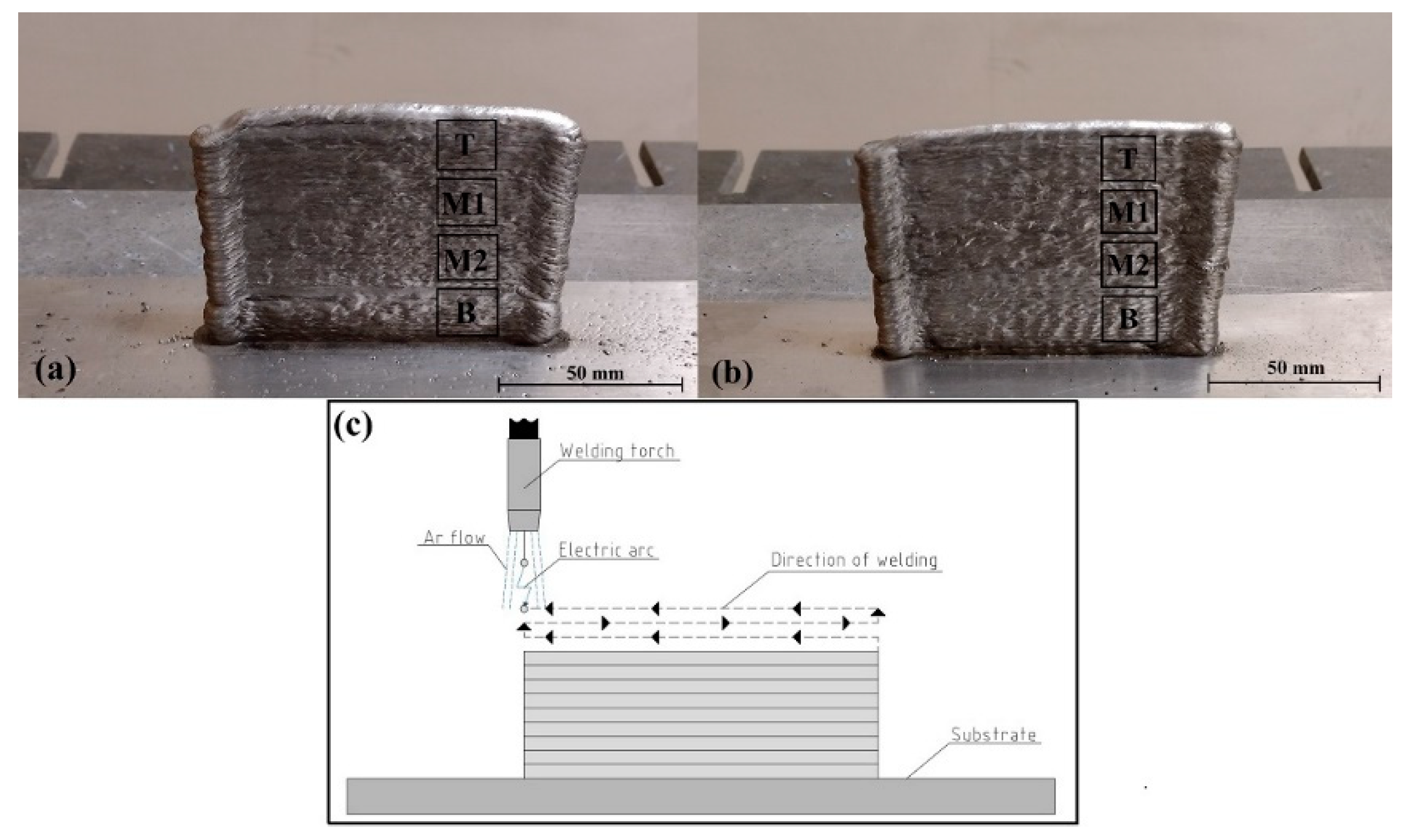
Two different specimens in the shape of thin walls, shown in Figure 1a,b with dimensions of 100 mm × 80 mm were manufactured using the GMAW technique Figure 1c, and implementing the cold arc pulse method. The shielding gas used during the experiments was Ar with a 99.999% purity and a flow rate of 17 l/min. The specimens were build-up at different welding speeds–13.3 mm/s and 20.0 mm/s, corresponding to the following heat inputs–120 J/mm and 80 J/mm. The heat input values were calculated using the heat input formula for MIG/MAG welding (Equation (1)) in agreement with the DIN EN ISO 15614-1 standard:
Q = (k×U×I)/v, [J/mm].
The heat input (Q) is in direct correlation to the input power (U.I), the welding speed (v), and the thermal efficiency of the welding process (k), which in the case of MIG/MAG welding is assumed to be 0.8. The wire feeding speed was 100 mm/s, the current was 117 A, and the voltage was 17.1 V. The pulse frequency correction control circuit was utilized and set to 10 kHz in the negative direction. The offset in the z-direction (the direction of specimen growth) was set to 0.85 mm per layer while using the 20.0 mm/s welding speed. The offset during the fabrication of the specimen build with the lower welding speed was set to 0.95 mm per layer.
The built specimens were cut into four different sections from the different stages of growth, marked as “T”, “M1”, “M2”, and “B”, corresponding to the top, middle, and bottom. The obtained samples, with dimensions of 15 × 15 mm, were covered in epoxy resin and the surface of each sample was mechanically processed in a step-by-step polishing pattern using abrasive paper sheets with the following grain sizes–P240, P400, P600, P800, P1200, and P2500. The mechanical polishing was followed by etching of the surface of the samples with a solution containing a 10% concentration of hydrofluoric acid (HF).
The phase composition and the texture of the samples was studied using X-ray diffraction (XRD) in a symmetrical Bragg-Bretano mode. The measurements were carried out using CuKα radiation with a wavelength of 1.5406 Ǻ in the range of 20 to 80 degrees of the 2θ scale. The structure of the samples is observed using both an optical microscope (Drawell MIT 300/500 series) and a scanning electron microscope (SEM) employing the backscattered electrons mode. The chemical composition as well as the concentration of Si in the manufactured specimens was also studied using energy dispersive X-ray spectroscopy (EDX).
The Vickers hardness at each individual growth stage of the specimens was obtained by a ZwickRoell Dura Scan 10/20 G5 hardness tester equipped with a pyramid shaped diamond indenter tip, and in agreement with the ISO 6507-2 standard. During the experiments, 15 consecutive measurements were taken with an applied contact force of 1N and a time of contact of 5 s.

3. Results

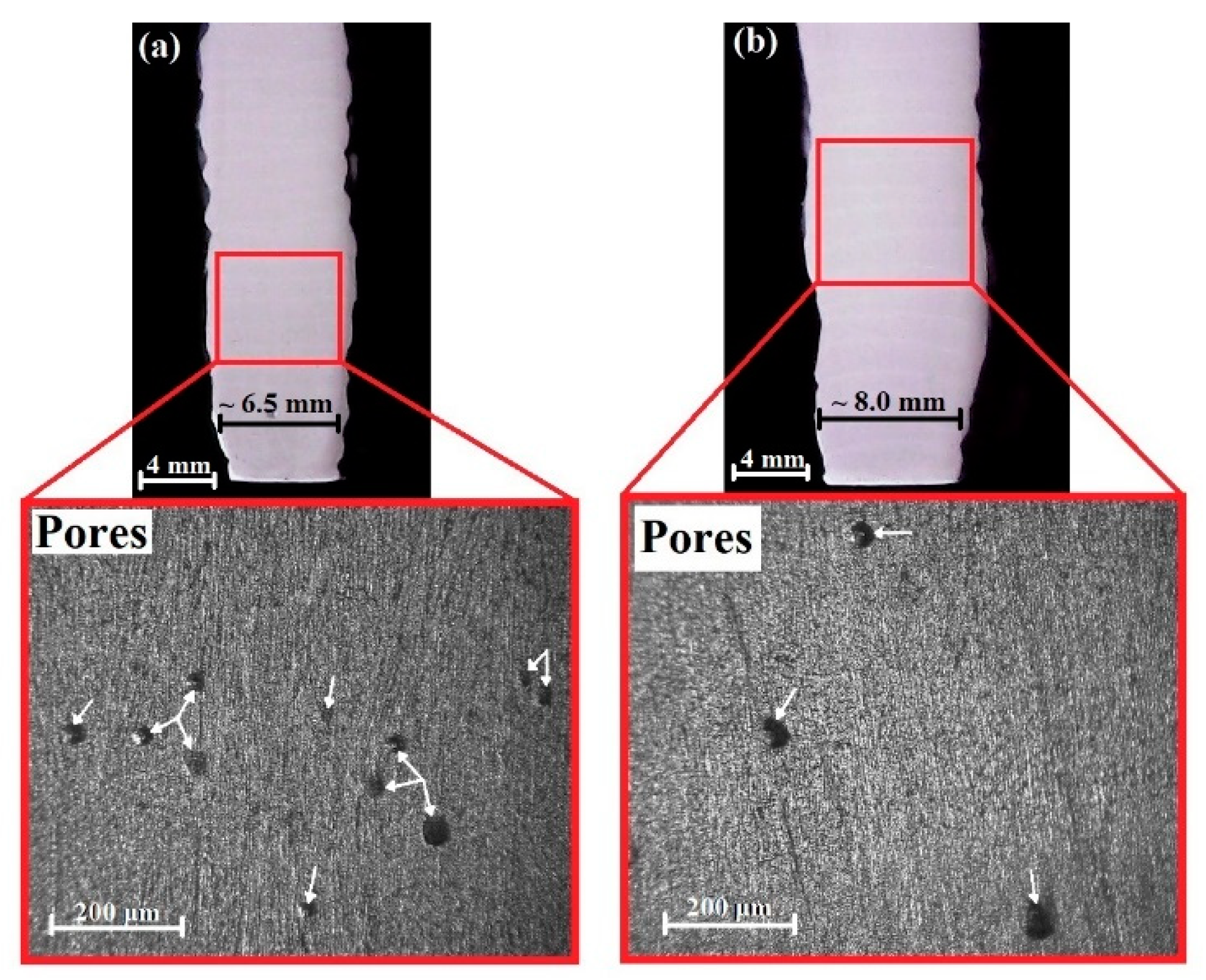
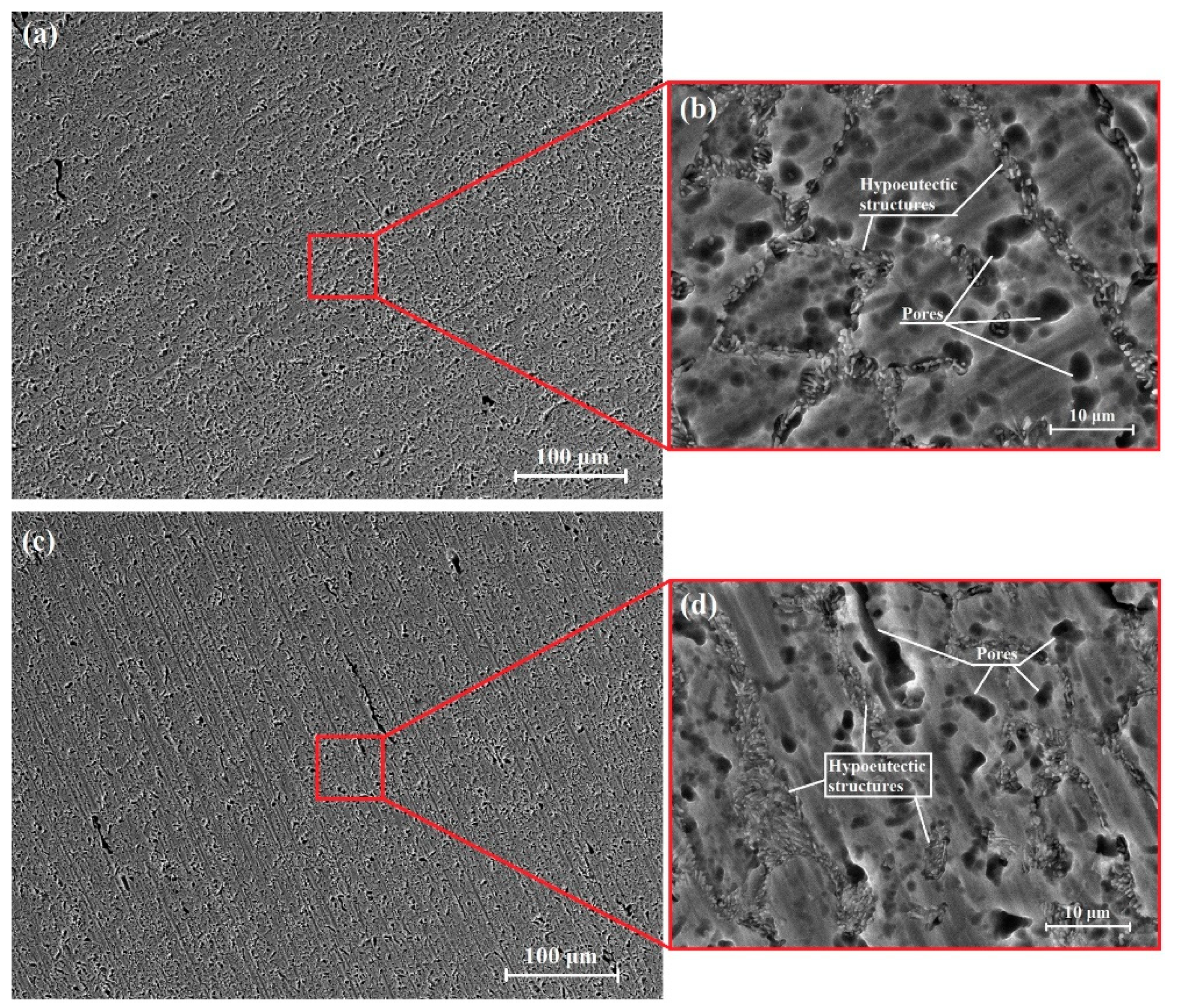
Preliminary observations of the microstructure of the samples were carried out using an optical microscope. Cross sectional samples taken from every stage of build-up were analyzed, indicating no significant change in the porosity level of each separate specimen at the different stages of growth. Due to this the images displayed in Figure 2a,b correspond only to the samples taken from the bottom (B) of each specimen and are indicative of the level of porosity observed in the entire cross section of each specimen. When comparing the two specimens a higher level of porosity is observed in the structure of the one built at a welding speed of 20 mm/s. This is caused by the shorter life of the weld pool in that case which impairs the diffusion of gases during the process of welding.
A noticeable difference in the thickness of the specimen is observed where the one build at a welding speed of 20.0 mm/s has a thickness of 6.5 mm on average, and the one build at a speed of 13.3 mm/s has a thickness of 8.0 mm on average. Despite the difference in thickness no further geometrical differences between the two specimens were detected.
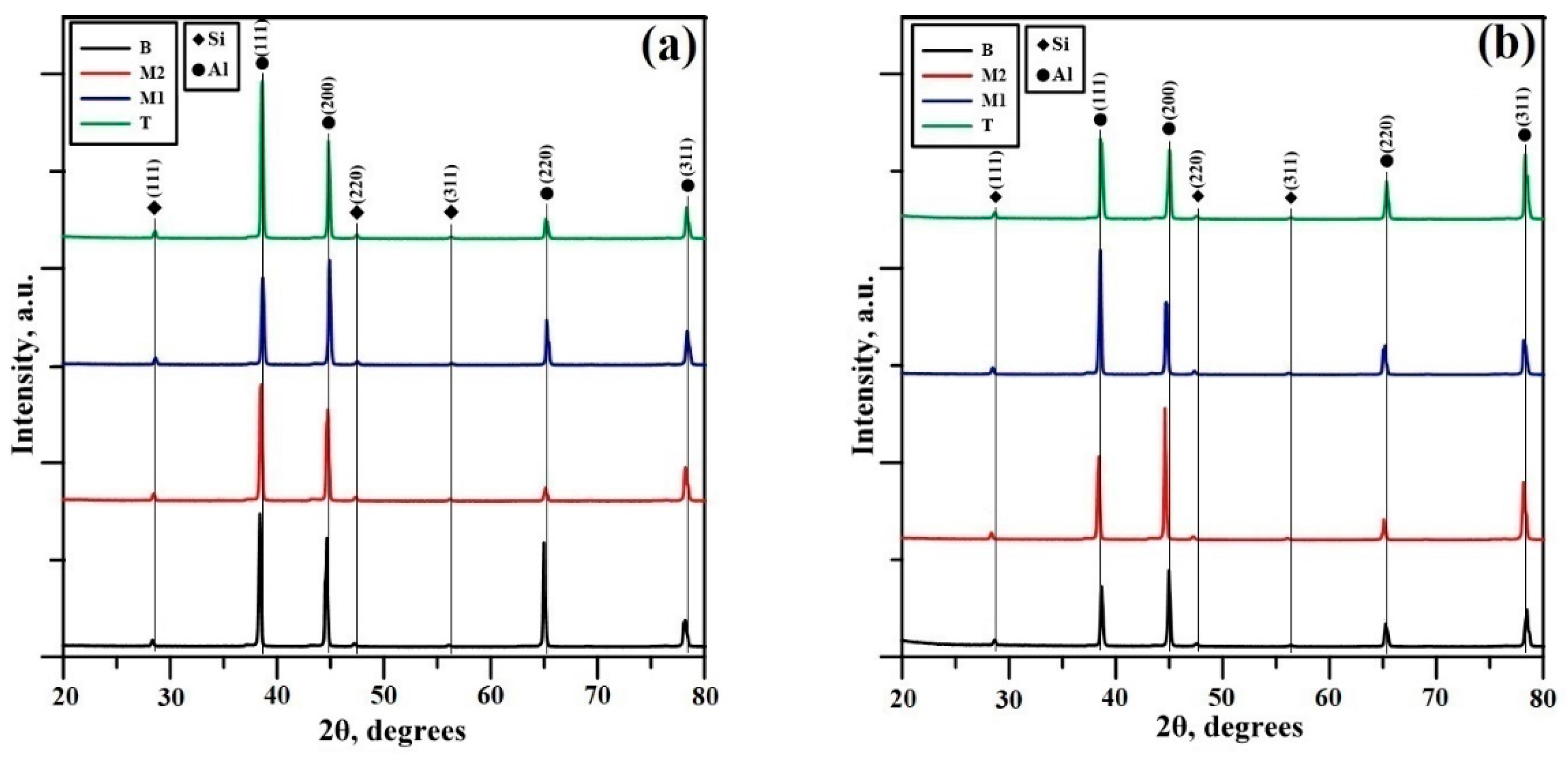
Following the study of the structure using an optical microscope an X-ray diffraction analysis was performed. The XRD results for all samples taken from both specimens built at different welding speeds are shown in Figure 3a,b. A double phase structure consisting of Al and Si peaks is detected. This type of configuration of the phase composition is characteristic for WAAM AlSi5 specimens as confirmed by Su et al. [21]. Both detected phases have a face-centered cubic structure (fcc).
The preferred crystallographic orientation in relation to the different stages of specimen growth was determined using the pole density (Phkl) [22], calculated using Equation (2):
Phkl = (Iexp/Ist)/[(1/n) × Σn(Iexp/Ist)],
where Iexp is the experimentally detected intensity of a certain diffraction maximum, Ist is a standard value taken from the crystallographic ICDD (international center for diffraction data) database, and n is the number of the studied peaks. The results are summarized in Table 2. In the case of the lower welding speed an initial preferred crystallographic orientation towards the (220) plane is detected at the bottom of the specimen, followed by a change in the preferred orientation towards the (200) plane. In the case of a welding speed of 20.0 mm/s a change in the preferred crystallographic orientation from the (200) plane towards the (311) plane is observed towards the upper parts of the specimen. These orientation shifts are attributed to the high thermodynamic nature of the arc welding process, where the aluminum alloy wire is heated beyond its’ melting point followed by a rapid solidification. This leads to a texture change in favor of the (200), (220), and (311) crystallographic planes. These results are in agreement to the results obtained by He et al. [23], who notice a change in the preferred crystallographic orientation of pure aluminum from the (111) plane towards the (200) plane after pressurizing and heating the samples to a temperature of 430 °C (700 K). The initial deposition temperature is in the range of 25–40 °C and increases with the increase of the specimens’ height [18]. Reportedly the (111) crystallographic orientation of aluminum and aluminum alloys is the most stable one corresponding to a highly dense structure. This crystallographic orientation of aluminum has the highest deformation resistance due to the higher density of that orientation [24]. Although the processes of texture control are still debatable it is obvious that the specimen built at a welding speed of 13.3 mm/s, the contribution of (111) is slightly higher, which is evidence for the formation of a denser structure with less amount of defects compared to the specimen built at a welding speed of 20.0 mm/s. During the process of welding using the speed of 13.3 mm/s, the aluminum atoms realign in a way that allows them to form a higher quantity of denser bonds resulting in higher inclusions of the (111) crystallographic orientation.
In order to study the change in the structural imperfections of the specimens in relation to their growth during the process of build-up the full width at half maximum (FWHM) of each obtained sample was calculated. The results are presented in Table 3.
According to the X-ray diffraction theory, the diffraction maximum broadening is a function of the crystallographic imperfections. In most cases an increase of the FWHM with the increase of the height of the specimens is observed, with exception of the results obtained for the peak corresponding to the (220) plane in the case of the higher welding speed. In that case an initial FWHM value of 0.3677 is obtained corresponding to the sample taken from the bottom (B) of the specimen, and a value of 0.2636 is obtained for the sample taken from the top (T). Vashita et al. [25] have observed the relation between the internal residual stress and the FWHM, suggesting an increase of the FWHM indicates a higher presence of internal strain in the structure, which leads to an increase of the concentration of defects. Studying the evolution of the crystallographic peaks we can conclude that their FWHM slightly increases at the more advanced stages of build-up in both cases. This corresponds to the higher cooling rate resulting in faster solidification of the molten material.
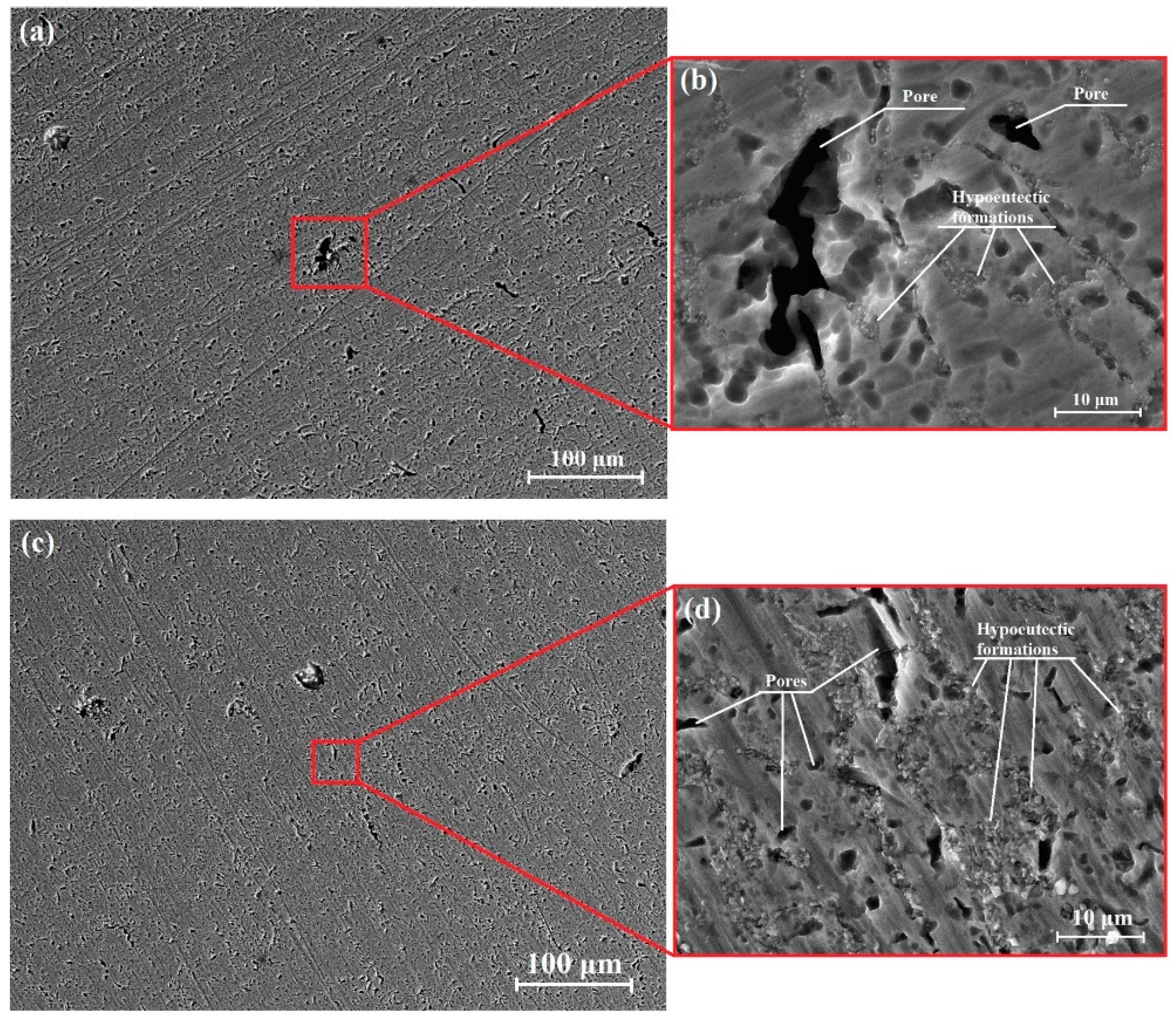
In order to further study, the structure of the specimens scanning electron microscopy is employed. Figure 4a,c depict larger scale images of samples “T” and “M2” taken from the specimen built at a welding speed of 20 mm/s. The images are taken in the backscattered electrons (BSE) mode. Figure 4b,d depict images of closer studied areas of the samples taken in the secondary electrons (SE) mode. Similarly Figure 5a,c show larger scale images of the samples “T” and “M2” taken from the specimen built at a welding speed of 13.3 mm/s in the backscattered electrons (BSE) mode, and Figure 5b,d show images of closer studied areas of the samples taken in the secondary electrons (SE) mode. Evidently, studying both specimens, a higher concentration of defects is observed in the structure of the samples taken from the specimen built at the higher welding speed. The observed defects are predominantly in the form of irregular solidification pores, which form due to the fast solidification nature of the weld pool during the process of arc welding [26]. These results are in agreement with the results obtained during the carried out optical microscopy and X-ray diffraction experiments. The microstructure of the specimens consists of pure aluminum fractions and αAl + Si eutectic (hypoeutectic) inclusions. A higher concentration of eutectic formations is detected in the case of the specimen built at the lower welding speed. Obviously, the lower welding speed leads to a higher material input per unit of time, causing an increase of the density of eutectic formations.
The chemical composition of the obtained samples was studied by the EDX mapping and the results are shown in Figure 6, Figure 7, Figure 8 and Figure 9. 
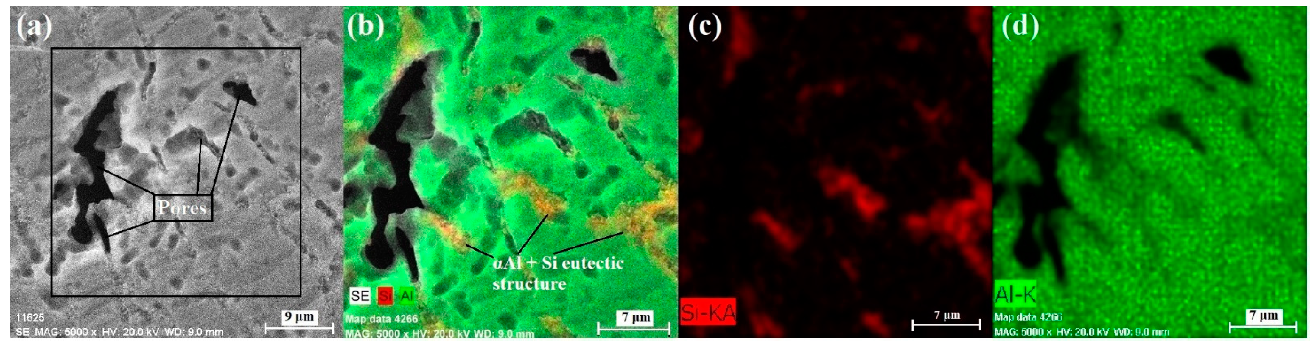
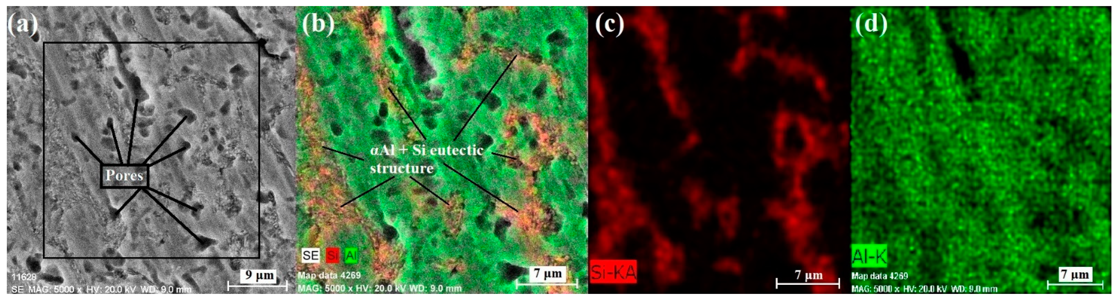
Figure 6a depicts a SEM image of the cross section of the sample taken from the top (T) of the specimen build at the higher welding speed of 20.0 mm/s using the backscattered electron (BSE) mode. High quantity of defects is observed in the structure of this part of the specimen in the form of pores. Figure 6b shows an EDX mapping of the squared zone in Figure 6a. The results of this experiment indicate a presence of 4.06 wt% of Si in the studied area. Furthermore, fibrous eutectic structures of αAl + Si are observed. The formation of this type of a double phase structure is typical for AlSi5 alloys [27]. Figure 6c depicts the Si component in the eutectic structures, and Figure 6d depicts the Al component in the structure.
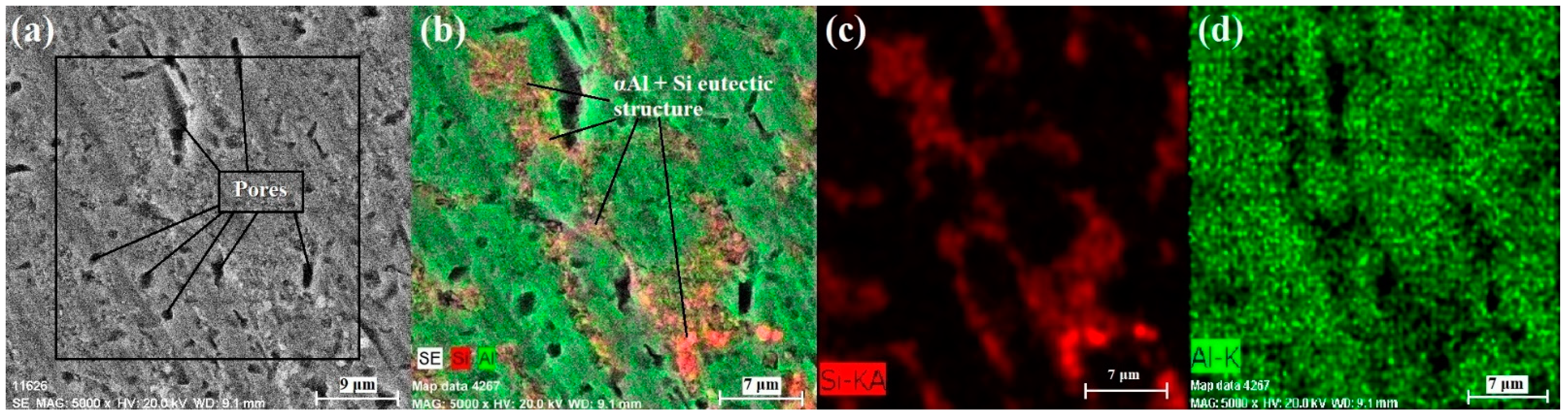
Figure 7a depicts a SEM image of the cross section of sample M2 taken from an area closer towards the bottom of the specimen build at the higher welding speed of 20 mm/s using the backscattered electron (BSE) mode. A highly porous structure is also detected in the structure of this sample. Figure 7b shows an EDX mapping of the squared zone in Figure 7a. The results of this experiment indicate a presence of 7.59 wt% of Si in the studied area. This amount of silicon is significantly higher compared to that at the top of the specimen, however, this can be attributed entirely to the depicted zone in Figure 6a, which has a large pore taking up most of the studied zone. In the case of sample M2, irregular eutectic structures of αAl + Si can be observed. Figure 7c depicts the Si component in the eutectic structures, and Figure 7d depicts the Al component in the structure.
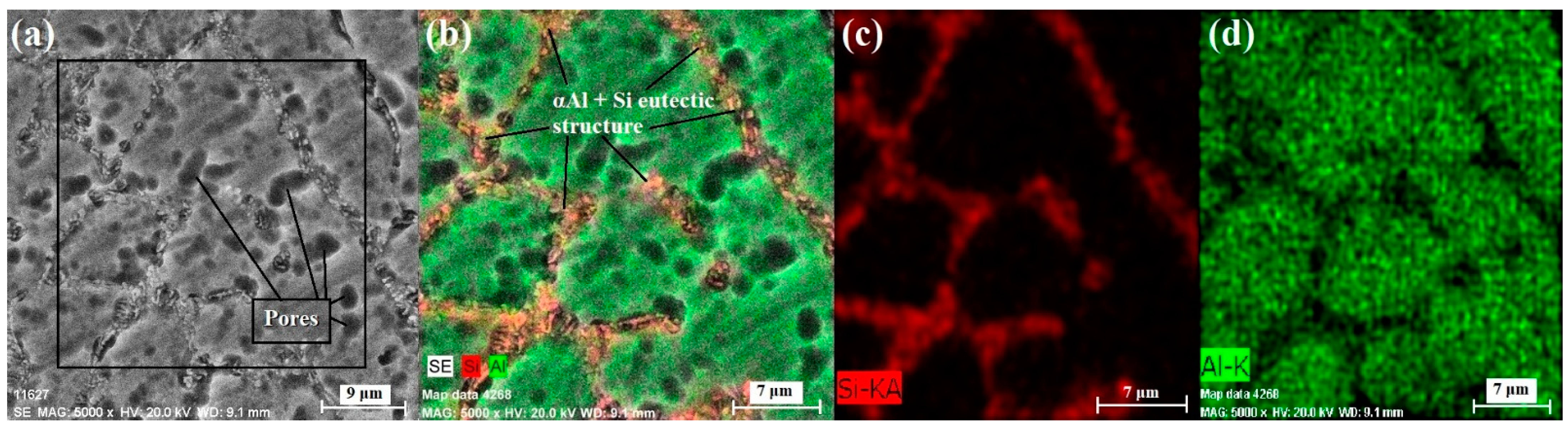
Figure 8a shows the obtained SEM micrograph for the sample taken from the top (T) part of the specimen built using the lower welding speed–13.3 mm/s. Figure 9a shows a SEM micrograph of a specimen taken from an area closer towards the bottom (M2) of the specimen built at the lower welding speed. A smaller size of the formed pores is detected in both cases as compared to the specimen built at the higher welding speed. Figure 8b and Figure 9b show an EDX mapping of the studied zone, where the already described eutectic aluminum silicon structures are colored in a brownish tint. A concentration of 6.23 wt% of Si is detected in the sample taken from the top of the specimen, and a concentration of 8.11 wt% of Si is detected closer towards the bottom of the specimen. This quantitatively proves the higher material input during the welding process compared to the specimen built at a speed of 20.0 mm/s. Furthermore, the same evolution of the eutectic formations is observed with the more advanced stages of build-up. The initially irregular structure transforms into a fibrous one at the top of the specimen. Figure 8 and Figure 9c,d show the silicon and aluminum components in the structure, respectively.
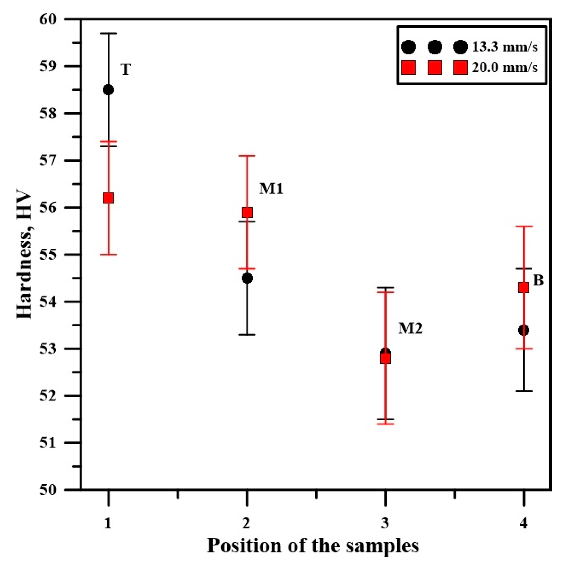
Figure 10 shows the results of the carried out Vickers hardness experiments. It is obvious that the hardness of the AlSi specimens is inhomogeneous at the different stages of growth. The initial hardness of the specimen built at a welding speed of 20.0 mm/s is about 54 HV0.1 ± 2.6 HV0.1, followed by a slight decrease to 53 HV0.1 ± 2.8 HV0.1. Then an increase of the hardness to about 56 HV0.1 ± 2.4 HV0.1 can be observed for both samples M1 and T. In the case of the specimen built at a speed of 13.3 mm/s its’ initial hardness is 53.5 HV0.1 ± 2.6 HV0.1, which also decreases to 53 HV0.1 ± 2.8 HV0.1. However, the hardness of the M1 sample is slightly lower compared to that of the specimen built using the higher welding speed. Its’ maximum hardness of 58.5 HV0.1 ± 2.4 HV0.1 was measured at the top (T) of the specimen. In any case the deviation of the hardness of the samples is very small with the difference between the lowest and highest detected values being just 8 HV0.1. These results are in agreement with the results reported by Tian et al. [28]. The variable hardness of the specimens seems to be characteristic for AlSi alloys. Similar results are also reported by [29] along with a possibility of increasing and equalizing the hardness of manufactured AlSi components by a subsequent heat treatment.

4. Discussion

The technological conditions of layer deposition are in direct correlation to the geometrical characteristics of the built components. Köhler et. al. [15] have studied the influence of the wire feeding speed and different thermal cycles on the geometrical characteristics of WAAM built Al5356 specimens in the CMT mode. They reported that the increase of the wire-feeding rate leads to the increase of the thickness of the specimens due to the higher quantity of the input material. Furthermore, the thickness of the specimens also increases with the advance of the build-up process due to the higher layer deposition temperature. The correlation between the pulse frequency correction factor and the geometry of WAAM built Al5183 specimen in the CMT mode is described in detail by Kang et al. [30]. Reportedly, with the increase of the negative pulse correction frequency, the width and height of the specimens increases. In addition, the decrease of the welding speed leads to the further increase of the width and height of the specimens [30]. All of the results described above are in agreement with the results obtained in this work. During the build-up of the specimens, a noticeable change in their thickness is observed in relation to the welding speed. The wall-shaped detail built with a welding speed of 20.0 mm/s has an average thickness of 6.5 mm, whereas the one built at a welding speed of 13.3 mm/s has an average thickness of 8.0 mm. This is caused by the constant wire-feeding rate which in the case of the slower welding process causes a higher aluminum input per pulse. The growth of the specimen is also directly correlated to the input of the electrode material. Due to the formation of a larger weld pool during welding at a speed of 13.3 mm/s, the growth of the specimen is increased along with its’ width. This poses the necessity of increasing the offset in the z direction after each layer deposition.
The welding speed also has a direct influence on the microstructure of the aluminum components. The porosity level in the case of both hydrogen entrapment caused pores and solidification pores of the samples manufactured with the lower welding speed is significantly lower compared to that of the samples taken from the specimen built using the higher welding speed. These results are confirmed by both the scanning electron microscopy results and the observations made with the optical microscope. Despite the significantly high flow rate of the protective gas (Ar in this case), small quantities of hydrogen can be adsorbed in the hot melt pool during the welding process. This leads to the formation of hollow gas cavities (pores) in the structure of the specimens. The formation of pores is highly undesirable since it leads to a significant deterioration of the mechanical properties of the specimen, particularly in regard to its’ shear strength [6]. The increase in the porosity level in the case of the higher welding speed is attributed to the lower lifetime of the weld pool due to the lower heat input. During the process of welding, any gases trapped in the structure of the specimen are diffused in the direction of specimen growth. This is caused since the zone containing a higher concentration of pores has a higher pressure compared to the newly formed one which has a lower pressure. This causes the gas molecules to migrate from the bottom of the weld pool towards its’ top. The diffusion of gases, however, is directly correlated to the heat input and the duration of the molten phase of the welded zone. The longer the duration of the molten phase is, the higher the rate of diffusion is. This leads to the significant reduction of the number of pores observed in the cross-section of the specimen.
The Vickers hardness analyses in the present study carried out at a load of 1 N indicate an average hardness of about 56 HV0.1 ±8 HV0.1 in the case of both specimens. It seems that such a hardness is characteristic for WAAM manufactured aluminum silicon alloys as reported by other researchers [28,29]. However, the obtained microhardness values are lower compared to those of cast aluminum alloys [27]. This is undoubtedly caused by the high heat input and significantly more rapid solidification of the alloy during the arc welding process resulting in the reorientation of the aluminum crystal structure from the denser (111) plane towards the more unstable (200), (220), and (311) planes. The increased contribution of these crystallographic orientations leads to the increase of the defects in the structure of the specimens leading to the decrease of their overall hardness. This is confirmed by the higher full width at half maximum of the aluminum peaks in the (200), (220), and (311) planes. The different contribution of the detected crystallographic planes signifies to the difference in the texture of each different sample which partly explains the inhomogeneous nature of the hardness of WAAM built AlSi5 specimens. Nikanorov et. al.[27] have studied the effect of different silicon contents on the mechanical properties of cast aluminum alloys and reported that with the increase of the silicon content the hardness and Young’s modulus of the specimens increase. In the present study, however, the exactly opposite tendency is observed. A decrease of the concentration of Si in the structure of each specimen per unit of area is observed with the more advanced stages of growth. In addition, a higher concentration of defects in the structure of both specimens is observed. The paradox, however, is the increase of the hardness of the specimens in that area, despite the higher concentration of defects and lower concentration of silicon. This is caused by the change in the type of the eutectic structures. Initially they are in the form of irregular formations due to the lower deposition temperature, thus the lower cooling rate. With the increase of the height of the specimens the influence of the water-cooled substrate decreases which leads to the increase of the layer deposition temperature. As it is known, an increase of the thermal input leads to the increase of the cooling rate, thus an increase of the solidification of the material. Due to the much higher thermal conductivity of aluminum compared to silicon, it has a much higher solidification speed [31]. This forces the silicon particles to take up the free space between the polycrystalline aluminum grains forming fibrous eutectic formations, which follow almost ideally the path of defects in the structure. This reinforces the aluminum matrix by reducing the mobility of defects in the structure of the alloy, which intern increases the coefficient of elastic deformation, which leads to the slight increase of the hardness [32]. These observations are in agreement with the obtained microhardness results as the samples taken from the top of each specimen have the highest detected values. The sample taken from the top of the specimen built at a welding speed of 20.0 mm/s has a lower hardness similar to that of the middle section of the specimen, due to the increased concentration of defects in the structure.
A highly known drawback to AlSi alloys is the necessity of subsequent heat treatment in order to form a highly homogenized structure. This leads to the major improvement of the mechanical characteristics of the alloy [33] but increases the production costs. Furthermore, any heat treatment of other materials and their alloys that may be included in the WAAM process and conjoined with the AlSi5 built structure may cause highly undesirable effects on them such as a degradation of some of the mechanical properties of the alloy such as the coefficient of plastic deformation, shear strength, hardness, wear resistance, etc. This stresses the importance of optimization of the process of wire arc additive manufacturing in order to manufacture components with sufficient technological characteristics, potentially omitting the necessity of subsequent heat treating.

5. Conclusions

In this study, two wire arc additively manufactured specimens were built using the gas metal arc welding (GMAW) method in the cold arc pulse mode implementing two welding speeds-13.3 mm/s and 20 mm/s in order to better understand the influence of the heat input on the structure and some mechanical properties of AlSi5 components. Observing the results obtained in this work the following conclusions can be made:
(1)
Both specimens have a double phase composition consisting of aluminum and silicon peaks with a face-centered cubic structure. The preferred crystallographic orientation of the specimen built at a speed of 13.3 mm/s is initially directed towards the (220) plane followed by a 45° unit cell shift towards the (200) crystallographic plane. In the case of a welding speed of 20 mm/s a preorientation from the (200) plane towards the (311) plane is observed towards the top of the specimen due to the increase of the deposition temperature. An increase of the FWHM, thus the concentration of defects, is observed parallel to the increase of the height of the specimens;
(2)
The lowering of the welding speed resulted in an increase of the thickness of the specimens. The density of αAl + Si eutectic formations in their structure was also increased. In addition, the lower welding speed increased the volume of the melt pool and the lifetime of liquid phase respectively, which improved the diffusion of gases and thus led to the decrease of the concentration of pores in the structure of the specimens;
(3)
Irregularly structured eutectic formations were observed at the initial stages of specimen growth in both cases. Since the deposition temperature increased at the more advanced stages of growth a higher cooling rate was observed, which led to the faster solidification of the melt pool. As it is known aluminum has a higher heat of fusion and a higher thermal conductivity compared to silicon, which explains its’ higher solidification rate. This causes a change in the structure of the αAl + Si eutectic formations from irregular to fibrous. The newly formed fibers occupy the space between the aluminum polycrystalline grains, where most of the defects in the structure are formed. This leads to the decrease of the mobility of defects in the aluminum matrix, which leads to the increase of the coefficient of elastic deformation. This intern leads to the slight increase of the hardness of the specimens.
The obtained results in this work explain the correlation between microstructure and microhardness of WAAM AlSi5 specimens using GMAW. This study can be used for the further optimization of the technological conditions of specimen build-up. The unification of the hardness of the specimens at the different stages of growth could omit the need for subsequent heat treatment of the formed components depending on their application, of course.

Author Contributions

Conceptualization, G.K., S.V., R.O. and N.D.; methodology, S.V., G.K., M.O., R.O., N.D., V.M.; validation, G.K., S.V., M.O., N.D.; formal analysis, G.K., M.O., A.N.; investigation, G.K., M.O., N.D., A.N.; data curation, G.K., M.O., A.N.; writing—original draft preparation, G.K.; writing—review and editing, S.V., G.K., N.D., V.M.; funding acquisition, S.V., R.O., V.M. All authors have read and agreed to the published version of the manuscript.

Funding

This research was funded by the Bulgarian National Science Fund, grant number KP 06-DO 02/1 (2019).

Data Availability Statement

Not applicable.

Conflicts of Interest

The authors declare no conflict of interest.

References

  1. Herzog, D.; Seyda, V.; Wycisk, E.; Emmelmann, C. Additive manufacturing of metals. Acta Mater. 2016, 117, 371–392. [Google Scholar] [CrossRef]
  2. Ngo, T.; Kashani, A.; Imbalzano, G.; Nguyen, K.; Hui, D. Additive manufacturing (3D printing): A review of materials, methods, applications and challenges. Compos. Part B 2018, 143, 172–196. [Google Scholar] [CrossRef]
  3. Frazier, W. Metal Additive Manufacturing: A Review. J. Mater. Eng. Perf. 2014, 23, 1917–1928. [Google Scholar] [CrossRef]
  4. DebRoy, T.; Wei, H.; Zuback, J.; Mukherjee, T.; Elmer, J.; Milewski, J.; Beese, A.; Wilson-Heid, A.; De, A.; Zhang, W. Additive manufacturing of metallic components—Process, structure and properties. Prog. Mater. Sci. 2018, 92, 112–224. [Google Scholar] [CrossRef]
  5. Wu, B.; Pan, Z.; Ding, D.; Cuiuri, D.; Li, H.; Xu, J.; Norrish, J. A review of the wire arc additive manufacturing of metals: Properties, defects and quality improvement. J. Manuf. Process. 2018, 35, 127–139. [Google Scholar] [CrossRef]
  6. Ramalho, A.; Santos, T.; Bevans, B.; Smoqi, Z.; Rao, P.; Oliveira, J. Effect of contaminations on the acoustic emissions during wire arc additive manufacturing of 316L stainless steel. Add. Manuf. 2022, 51, 102585. [Google Scholar] [CrossRef]
  7. Rodrigues, T.; Escobar, J.; Shen, J.; Duarte, V.; Ribamar, G.; Avila, J.; Maawad, E.; Schell, N.; Santos, T.; Oliveira. Effect of heat treatments on 316 stainless steel parts fabricated by wire and arc additive manufacturing: Microstructure and synchrotron X-ray diffraction analysis. Add. Manuf. 2021, 48, 102428. [Google Scholar] [CrossRef]
  8. Li, S.; Li, J.; Jiang, Z.; Cheng, Y.; Li, Y.; Tang, S.; Leng, J.; Chen, H.; Zou, Y.; Zhao, Y.; et al. Controlling t he columnar-to-equiaxed transition during Directed Energy Deposition of Inconel 625. Add. Manuf. 2022, 57, 102958. [Google Scholar] [CrossRef]
  9. Hauser, T.; Reisch, R.; Breese, P.; Lutz, B.; Pantano, M.; Nalam, Y.; Bela, K.; Kamps, T.; Volpp, J.; Kaplan, A. Porosity in wire arc additive manufacturing of aluminum alloys. Addit. Manuf. 2021, 41, 101993. [Google Scholar] [CrossRef]
  10. Norrish, J.; Cuiuri, D. The controlled short circuit GMAW process: A tutorial. J. Manuf. Process. 2014, 16, 86–92. [Google Scholar] [CrossRef]
  11. Kah, P.; Suoranta, R.; Martikainen, J. Advanced gas metal arc welding processes. Int. J. Adv. Manuf. Technol. 2013, 67, 655–674. [Google Scholar] [CrossRef]
  12. Ayarkwa, K.; Williams, S.; Ding, J. Investigation of pulse advance cold metal transfer on aluminum wire arc additive manufacturing. Int. J. Rapid. Manuf. 2015, 5, 44–57. [Google Scholar] [CrossRef]
  13. Chen, T.; Xue, S.; Wang, B.; Zhai, P.; Long, W. Study on Short-Circuiting GMAW Pool Behaviour and Microstructure of the Weld with Different Waveform Control Methods. Metals 2019, 9, 1326. [Google Scholar] [CrossRef] [Green Version]
  14. Matusiak, J.; Pfeifer, T. The research of technological and environmental conditions during low-energetic gas-shielded metal arc welding of aluminum alloys. Welding Int. 2013, 27, 338–344. [Google Scholar] [CrossRef]
  15. Kumar, M.; Manikandan, M. Assessment of Process, Parameters, Residual Stress Mitigation, Post Treatments and Finite Element Analysis Simulations of Wire Arc Additive Manufacturing Technique. Met. Mater. Int. 2022, 28, 54–111. [Google Scholar] [CrossRef]
  16. Veiga, F.; Suarez, A.; Aldalur, E.; Bhujangrao, T. Effect of the Metal Transfer Mode on the Symmetry of Bead Geometry in WAAM Aluminum. Symmetry 2021, 13, 1245. [Google Scholar] [CrossRef]
  17. Köhler, M.; Fiebig, S.; Hensel, J. Wire and Arc Additive Manufacturing of Aluminum Components. Metals 2019, 9, 608. [Google Scholar] [CrossRef] [Green Version]
  18. Köhler, M.; Hensel, J.; Dilger, K. Effects of Thermal Cycling on Wire and Arc Additive Manufacturing of Al-5356 Components. Metals 2020, 10, 952. [Google Scholar] [CrossRef]
  19. Geng, Y.; Panchenko, I.; Chen, X.; Ivanov, Y.; Konovalov, S. Investigation of Microstructure and Fracture Mechanism of Al-5.0Mg Alloys Fabricated by Wire Arc Additive Manufacturing. J. Mater. Eng. Perf. 2021, 30, 7406–7416. [Google Scholar] [CrossRef]
  20. Sun, J.; Hensel, J.; Köhler, M.; Dilger, K. Residual stress in wire and arc additively manufactured aluminum components. J. Mater. Process. 2021, 65, 97–111. [Google Scholar] [CrossRef]
  21. Su, C.; Chen, X.; Konovalov, S.; Singh, R.; Jayalakshmi, S.; Huang, L. Effect of Deposition Strategies on the Microstructure and Tensile Properties of Wire Arc Additive Manufactured Al-5Si Alloys. J. Mater. Eng. Perf. 2021, 30, 2136–2146. [Google Scholar] [CrossRef]
  22. Valkov, S.; Kotlarski, G.; Ormanova, M.; Doynov, N.; Ossenbring, R.; Petrov, P.; Michailov, V. Crystallographic structure and mechanical properties of wire arc additively manufactured Al5356 components. C. R. Acad. Bulg. Sci. 2021, 74, 820–827. [Google Scholar] [CrossRef]
  23. He, D.; Zhao, Y.; Daemen, L.; Qian, J.; Lokshin, K.; Shen, T.; Zhang, J.; Lawson, A. Thermoelastic and texture behavior of aluminum at high pressure and high temperature investigated by in situ neutron diffraction. J. Appl. Phys. 2004, 95, 4645–4650. [Google Scholar] [CrossRef]
  24. Wang, X.; Shen, B.; Deng, L.; Li, J. Effects of original orientation combination on substructure characteristics during continuous dynamic recrystallization in an extruded Al-Cu-Li alloy. Mat. Char. 2017, 130, 113–122. [Google Scholar] [CrossRef]
  25. Vashista, M.; Paul, S. Correlation between full width at half maximum (FWHM) of XRD peak with residual stress on ground surfaces. Phil. Mag. 2012, 92, 4194–4204. [Google Scholar] [CrossRef]
  26. Tawfik, M.; Nemat-Alla, M.; Dewidar, M. Enhancing the properties of aluminum alloys fabricated using wire + arc additive manufacturing technique—A review. J. Mater. Res. Tech. 2021, 13, 754–768. [Google Scholar] [CrossRef]
  27. Nikanorov, S.P.; Volkov, M.; Gurin, V.; Burenkov, Y.; Derkachenko, L.; Kardashev, B.; Regel, L.; Wilcox, W. Structural and mechanical properties of Al-Si alloys obtained by fast cooling of a levitated melt. Mat. Sci. Eng. A 2005, 390, 63–69. [Google Scholar] [CrossRef]
  28. Tian, Y.; Shen, J.; Hu, S.; Wang, Z.; Gou, J. Microstructure and mechanical properties of wire and arc additive manufactured Ti-6Al-4V and AlSi5 dissimilar alloys using cold metal transfer welding. J. Manuf. Process. 2019, 46, 337–344. [Google Scholar] [CrossRef]
  29. Neuser, M.; Grydin, O.; Frolov, Y.; Schaper, M. Influence of solidification rates and heat treatment on the mechanical performance and joinability of the cast aluminum alloy AlSi10Mg. Prod. Eng. 2022, 16, 193–202. [Google Scholar] [CrossRef]
  30. Lee, T.; Kim, C.; Kang, M. Effects of Electrode Negative Pulsing Ration in Direct Energy Deposition via Variable-Polarity Cold Metal Transfer Process on the Deposition Behavior and Microstructural Characteristics. Metals 2022, 12, 475. [Google Scholar] [CrossRef]
  31. Makhlouf, M.; Guthy, H. The aluminum-silicon eutectic reaction: Mechanisms and crystallography. J. Light Met. 2001, 1, 199–218. [Google Scholar] [CrossRef]
  32. Barrirero, J. Eutectic Modification of Al-Si Casting Alloys; Linköping University: Linköping, Sweden, 2019. [Google Scholar]
  33. Sjölander, S.; Seifeddine, S. The heat treatment of Al-Si-Cu-Mg casting alloys. J. Mater. Process. 2010, 210, 1249–1259. [Google Scholar] [CrossRef]
Figure 1. WAAM specimens, and their corresponding sample positions, built at a welding speed of 13.3 mm/s (a), and 20.0 mm/s (b) using gas metal arc welding (c).
Metals 12 01870 g001
Figure 2. Optically detected pores in the cross sectional area of samples: (a) 20.0 mm/s, and (b) 13.3 mm/s, taken from the bottom position (B) of the specimens.
Metals 12 01870 g002
Figure 3. X-ray diffraction results at the different stages of growth of the specimens build-up at a welding speed of: (a) 13.3 mm/s; (b) 20.0 mm/s.
Metals 12 01870 g003
Figure 4. Cross-sectional SEM micrographs of the specimen built at a welding speed of 20.0 mm/s: larger scale micrographs of samples T (a) and M2 (c) taken in the BSE mode, and closer studied areas of both samples (b,d) taken in the SE mode.
Metals 12 01870 g004
Figure 5. Cross sectional SEM micrographs of the specimen built at a welding speed of 13.3 mm/s: larger scale micrographs of samples T (a) and M2 (c) taken in the BSE mode, and closer studied areas of both samples (b,d) taken in the SE mode.
Metals 12 01870 g005
Figure 6. Sample “T” taken from the specimen at a welding speed of 20.0 mm/s: (a) SEM micrograph of the studied zone; (b) EDX mapping; (c) silicon content detected; (d) aluminum content detected.
Metals 12 01870 g006
Figure 7. Sample “M2” taken from the specimen build at a welding speed of 20.0 mm/s: (a) SEM micrograph of the studied zone; (b) EDX mapping; (c) silicon content detected; (d) aluminum content detected.
Metals 12 01870 g007
Figure 8. Sample “T” taken from the specimen build at a welding speed of 13.3 mm/s: (a) SEM micrograph of the studied zone; (b) EDX mapping; (c) silicon content detected; (d) aluminum content detected.
Metals 12 01870 g008
Figure 9. Sample “M2” taken from the specimen build at a welding speed of 13.3 mm/s: (a) SEM micrograph of the studied zone; (b) EDX mapping; (c) silicon content detected; (d) aluminum content detected.
Metals 12 01870 g009
Figure 10. Vickers hardness of the samples taken from both specimens.
Metals 12 01870 g010
Table 1. Chemical composition of the substrate and the welding wire in wt%.
AlloyAlSiFeCuMnMgZnBeTiCrOthers
AlSi5Bal.4.5–5.50.60.30.150.20.10.00030.15-0.15
Al6082T6Bal.1.20.50.10.40.60.2-0.10.250.15
Table 2. Preferred crystallographic orientation in relation to the specimens’ growth.
Position in the SpecimenPhkl, %
P111P200P220P311
13.3 mm/s
T26.835.415.522.3
M113.233.931.321.6
M222.737.912.027.4
B14.024.449.811.8
20.0 mm/s
T11.922.025.940.2
M122.327.724.026.0
M211.940.113.634.4
B12.633.621.832.0
Table 3. Full width at half maximum (FWHM) of the detected peaks.
Material and Detected PlaneFWHM
13.3 mm/s
TM1M2B
Al (111)0.26010.26180.21110.2120
Al (200)0.26150.21080.26160.2626
Al (220)0.31410.26260.31510.2411
Al (311)0.36770.42020.31510.4220
20.0 mm/s
Al (111)0.26240.21330.21010.2121
Al (200)0.26260.26250.21120.2107
Al (220)0.26360.31510.31930.3677
Al (311)0.36760.36770.26280.3151
Publisher’s Note: MDPI stays neutral with regard to jurisdictional claims in published maps and institutional affiliations.

