Article

Effect of Proton Irradiation on the Defect Evolution of Zr/Nb Nanoscale Multilayers

1
Division for Experimental Physics, National Research Tomsk Polytechnic University, Tomsk 634050, Russia
2
Dzhelepov Laboratory of Nuclear Problems, Joint Institute for Nuclear Research, Dubna 141983, Russia
3
Department of Structural Research, Institute of Nuclear Physics Polish Academy of Sciences, PL-31342 Krakow, Poland
4
Institute of Electrophysics and Radiation Technologies, NAS of Ukraine, Chernyshevsky St. 28, 61002 Kharkov, Ukraine
*
Author to whom correspondence should be addressed.
Metals 2020, 10(4), 535; https://doi.org/10.3390/met10040535
Submission received: 31 March 2020 / Revised: 15 April 2020 / Accepted: 18 April 2020 / Published: 21 April 2020
(This article belongs to the Special Issue 10th Anniversary of Metals: Metallurgy and Metal Technology)

Abstract

:
Nanoscale multilayer coatings (NMCs) with different crystal structures are considered as capable of self-healing after radiation damage due to the recombination of vacancies and interstitials. This work is focused on a defect distribution study of NMCs based on Zr/Nb layers (25/25 nm and 100/100 nm) after proton irradiation. Coatings with a total thickness of 1.05 ± 0.05 µm were irradiated by 900-keV protons using a pelletron-type electrostatic accelerator with an ion current of 2 µA for durations of 60 min to 120 min. The influence of the irradiation effect was studied by X-ray diffraction analysis (XRD), glow discharge optical emission spectrometry (GD–OES), and Doppler broadening spectroscopy using a variable energy positron beam. The results obtained by these methods are compatible and indicate that defect concentration of Zr/Nb NMCs remains unchanged or slightly decreases with increasing irradiation time.

1. Introduction

Radiation-induced defects and the corresponding changes in mechanical properties in irradiated materials have been carefully studied in recent decades for various multilayer coatings [1,2,3,4,5,6,7]. These structures with various crystal structures are widely used as self-healing coatings in radiation point defects, where vacancies and interstitials can recombine [8,9,10,11]. Based on this concept, metals with various crystal structures (bcc, fcc, and hcp) were combined to produce nanoscale multilayer coatings (NMCs) with increased tolerance to radiation damage caused by He ion and proton bombardment.
Most of the previous studies have been devoted to multilayer fcc/bcc systems such as Cu/Nb [12], V/Ag [13], Cu/W [14], and Ni/Fe [15], since the large mismatch of the lattice parameters of the fcc/bcc interfaces increases the ability to store defects in NMCs [16].
Recently, NMCs based on hcp/bcc systems have begun to attract attention: Mg/Nb [8], Zr/Nb [17,18,19], Co/Mo [9], Mg/Ti [10], Cu/Zr [20], etc. Most studies of hcp-based NMCs are focused on the relationship between the structural and strength characteristics of as-deposited nanoscale layers. However, there are only a few studies on the defect structure evolution of the hcp-based NMCs before and after irradiation [6,7]. The Zr/Nb multilayer system is regarded as promising for the creation of radiation-tolerant composite nanomaterials for the following reasons: both Zr and Nb are elements with a low thermal neutron capture cross-section, and are widely used in structural materials. Zr and Nb have different crystal lattices of hcp and bcc, respectively. The discrepancy between the parameters and types of the lattices is sufficient to form incoherent or semi-coherent interfaces that act as sinks for irradiation defects [21]; the Zr/Nb system can form immiscible and thermostable interfaces. To understand whether the proton irradiation recovery process occurs in the hcp/bcc system, the Zr/Nb multilayers were subjected to this exposure.
The positron annihilation spectroscopy (PAS) method is a promising nuclear physical method for investigation and control of structural defects in multilayer coatings. Due to the phenomenon of “positron capture by defects”, this tool has become for today the most sensitive instrument for open-volume defect study among all existing methods traditionally used in material science (TEM, XRD, and so on) [22]. The effectiveness of using the PAS method to study radiation defects and multilayer coatings has been demonstrated in many papers [23,24,25,26,27,28,29]. Topical issues that can be solved by using the PAS method are the study of mechanisms and dynamics of appearance, transformation, and elimination of defects on irradiation of charged particles.
The aim of this work is the experimental study of defect evolution and the crystalline structure of Zr/Nb multilayer system after proton irradiation for the design of radiation-tolerant materials.

2. Materials and Research Methods

The Zr/Nb NMCs were deposited on single-crystal Si (110) substrate via direct current (DC) magnetron sputtering. The residual pressure in the vacuum chamber was 10−3 Pa. Before deposition, the Si substrates were etched by Ar ions at 0.1 Pa for 15 min. For deposition, two balanced magnetrons (90 mm in diameter) with Zr (99.95%) and Nb (99.9%) targets equipped with a DC power supply (APEL-M-5PDC, Tomsk, Russia) were used. The operation pressure was 0.25 Pa (Ar), while the distance from targets to the substrate was 100 mm. The target power density was 15 W/cm2 [30,31]. The Zr/Nb NMCs with individual layer thickness of about 100 ± 10 nm (named as Zr/Nb100) and 25 ± 2 nm (named as Zr/Nb25) were deposited. A total thickness of coatings was 1.05 ± 0.05 µm. After deposition, the substrates with Zr/Nb multilayers were cut into 10 mm × 10 mm plates and exposed to a perpendicular 900-keV H+ beam for 60, 90, and 120 min with ion current of about 2 µA. Thus, the radiation dose was in the range from 9 × 10¹⁶ to 1.8 × 10¹⁷ ion/cm2. Irradiation was performed on the pelletron-type electrostatic accelerator with a magnetic energy analyzer. An 11 µm thickness aluminum energy degrader covered the samples of Zr/Nb NMCs. The proton energy and foil thickness were chosen according to the SRIM calculation to place the Bragg peak position and stop the majority of ions in NMCs. This part of the research was performed at the large-scale IRT-T research reactor facility (Tomsk, Russia).
The cross-section of samples was observed by scanning electron microscopy in secondary electron mode using Mira II (Tescan, Brno, Czech Republic). The structural evolution of native and irradiated Zr/Nb multilayers was investigated by X-ray diffraction on a Shimadzu XRD-7000S diffractometer (Shimadzu, Kyoto, Japan) in a Bragg-Brentano (Theta-2Theta) configuration with Cu Kα radiation (λ = 0.154 nm) [32]. The layer-by-layer distribution of the Zr and Nb elements was investigated using glow discharge optical emission spectrometry [33,34]. GD–OES is a method with a high depth resolution and low detection limit of chemical elements. The depth profiling was carried out on a GD-Profiler 2 (Jobin Yvon Emission Horiba Group, France) with a 4 mm anode using the following parameters: pressure, 650 Pa; power, 40 W; frequency, 4 kHz; duty cycle, 25%. The electrical resistivity of unirradiated and irradiated Zr/Nb NMCs was measured using the four-point probe technique conducted at a temperature of 20 °C [35].
The defect-free reference, as well as the irradiated samples, were studied using the PAS method, Doppler broadening of the annihilation line (DBAL) using the variable positron energy at the JINR DLNP in Dubna, Russia [36,37]. A monoenergetic flux of positrons with a diameter of 5 mm with an intensity of 106 e+/s was used. The energy range of the implanted positron ranged from 0.1 keV to 36 keV. Annihilation γ radiation was detected by an HPGe detector (model GEM25P4-70 AMETEK ORTEC, USA) with an energy resolution of 1.20 keV, interpolated for the energy of 511 keV. The obtained DBAL spectra were analyzed by extracting the S and W parameters, defined as the zone below central or wing part of annihilation line divided by total area below this line, respectively. The S parameter represents numbers of positrons which annihilate with low-energy electrons and increase with defect concentration (CD). In contrast, the W parameter decreases with CD and annihilate with high-momentum electrons.
Most applications of positron beams require knowledge of the implantation characteristics for an appropriate interpretation of the experimental data. It is generally recognized that the positron implantation profile for a monoenergetic positron beam in a semi-infinite solid can be expressed by the Gaussian derivative, which is described in general terms by the so-called Makhovian profile:
P ( z ) = m × z m 1 z 0 m × e x p ( ( z z 0 ) m ) ,
where z is the depth of penetration of the positron from the surface; and m and z0 are parameters that are determined experimentally for each material [38].
It is well known that only z0 depends on the energy of the positron implant E (in keV) as follows:
z 0 = A ρ × Γ ( 1 + 1 m ) × E n ,
where ρ is the density of the material; A and n are constants; and Γ is the Gamma function, which can be expressed as:
Γ ( z ) = 0 x z 1 e x d x ;
The parameter z0 can be associated with mean positron implantation depth z according to the formula:
z = Γ ( 1 + 1 m ) × z 0 .

3. Results and Discussion

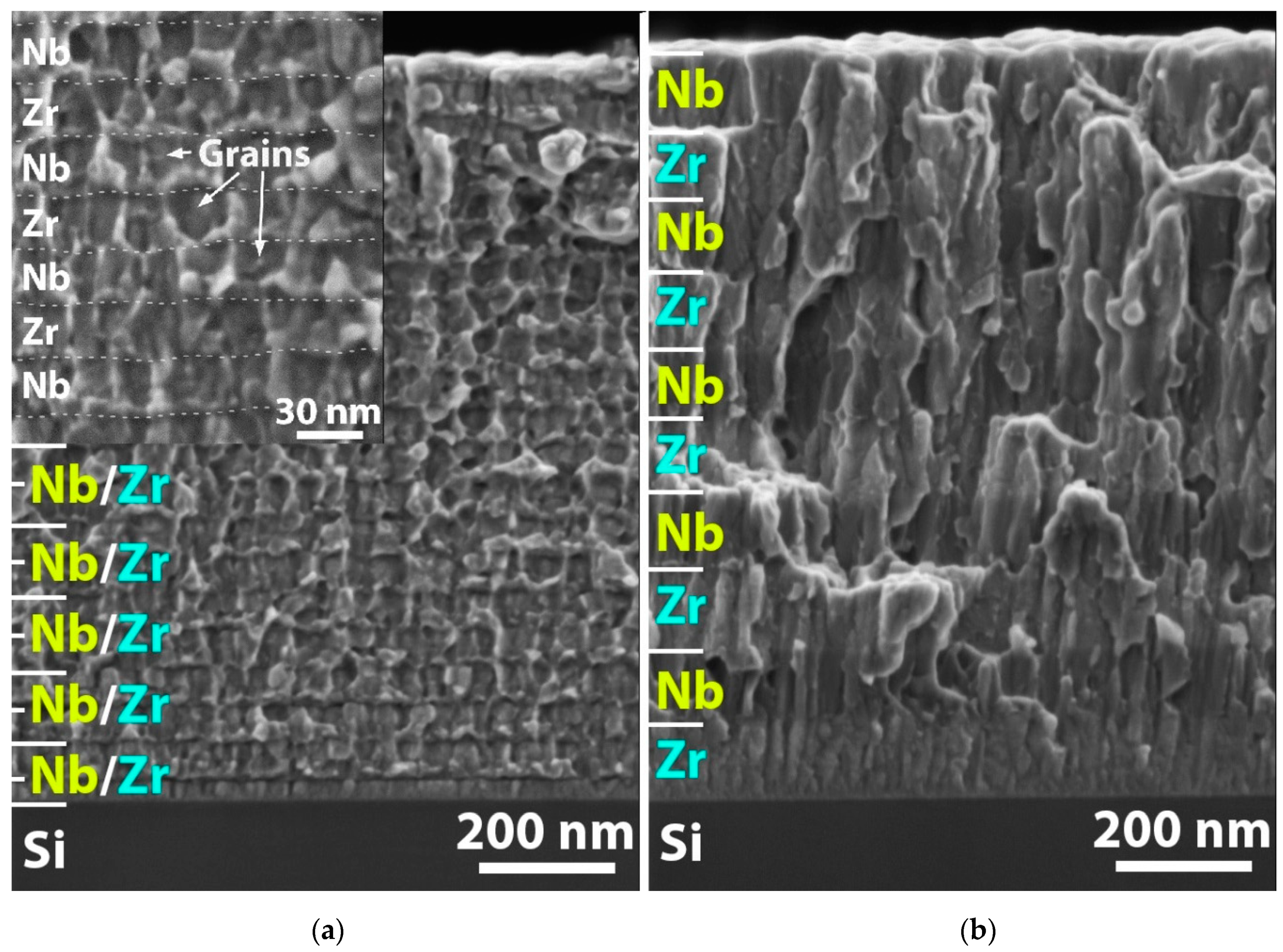
3.1. SEM of As-Deposited Zr/Nb Multilayer Coatings

Figure 1 shows the microstructures of the as-deposited Zr/Nb coatings with layer periodicities of 25 nm (Zr/Nb25) and 100 nm (Zr/Nb100). Analysis of the thickness measurements in different areas showed that the total thickness for both coatings was 1.05 ± 0.05 μm. Minor deviations in thickness of individual layers (up to approximately 10%) were observed. The grain size of the Zr/Nb25 coating did not exceed the thickness of the individual layers (Figure 1a). The Zr/Nb100 coating had a pronounced columnar structure in which grains continued to grow from one layer to another (Figure 1b). The width of the columns increased as the coating grew. The individual layer boundaries were visible for the Zr/Nb25 coating. In contrast, the layer boundaries for the Zr/Nb100 coating were mostly determined by contrast due to the difference in Zr and Nb densities. However, it should be noted that in the final layers of the Zr/Nb25, the boundaries became hardly distinguishable. In general, it can be concluded that an increase in periodicity (reduction of monolayer thickness) leads to inhibited grain growth and a less pronounced column structure of the coating.

3.2. SRIM Calculations

The SRIM-2013 [39] calculation of H+ irradiation was performed on Zr/Nb multilayered systems with individual layer thicknesses of 25 nm and 100 nm and a total thickness of 1 µm (Figure 2). The simulation was carried out using ion distribution and a quick calculation of damage mode with perpendicular 900 keV H+ beam, where the total number of incident particles was 5 × 10⁵. The presence of an 11 μm aluminum energy degrader was taken into account.
The simulation shows that the chosen energy and energy degrader thickness provided H+ implantation with deposition peak at depth of approximately 800 nm below the surface of the coating. Due to the difference in stopping power of Zr and Nb, there were dips and peaks on the graph that corresponded to Zr and Nb layers. A small number of ions were stopped in the Si substrate. Nonetheless, the majority of ions were stopped in the Zr/Nb NMC.

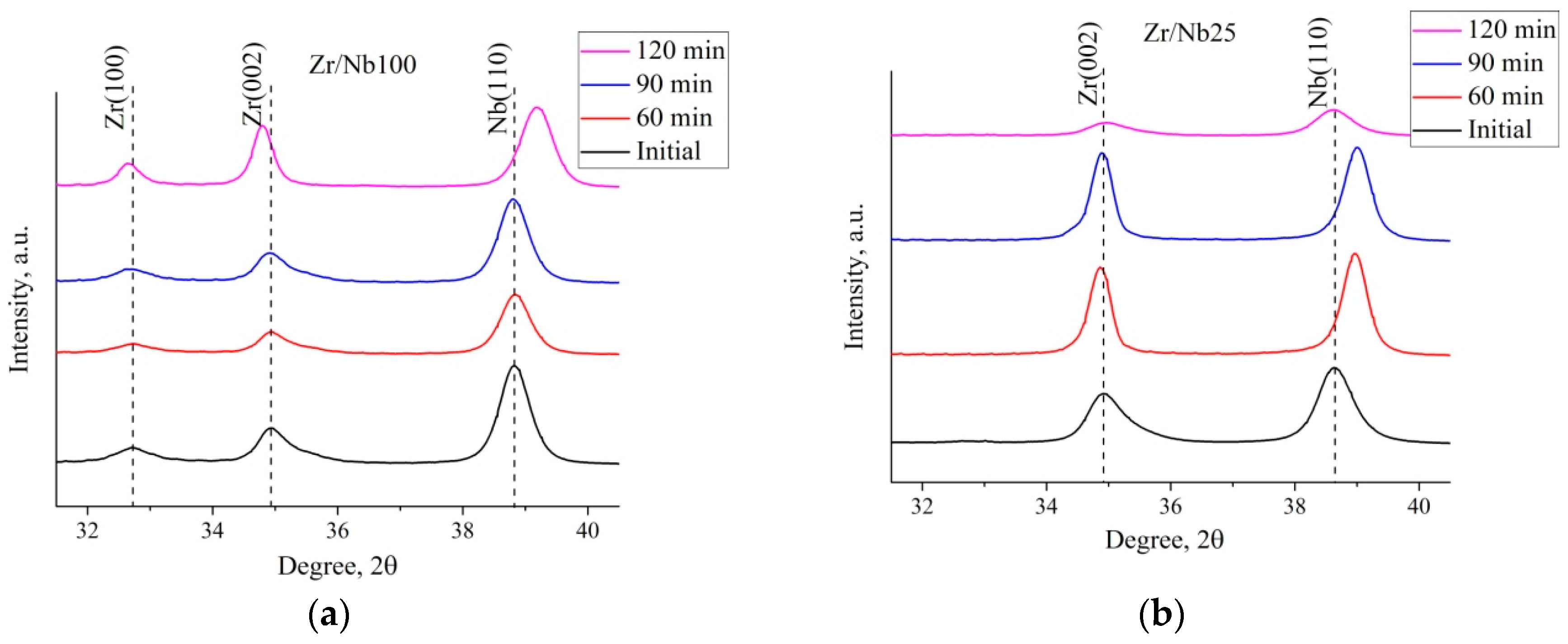
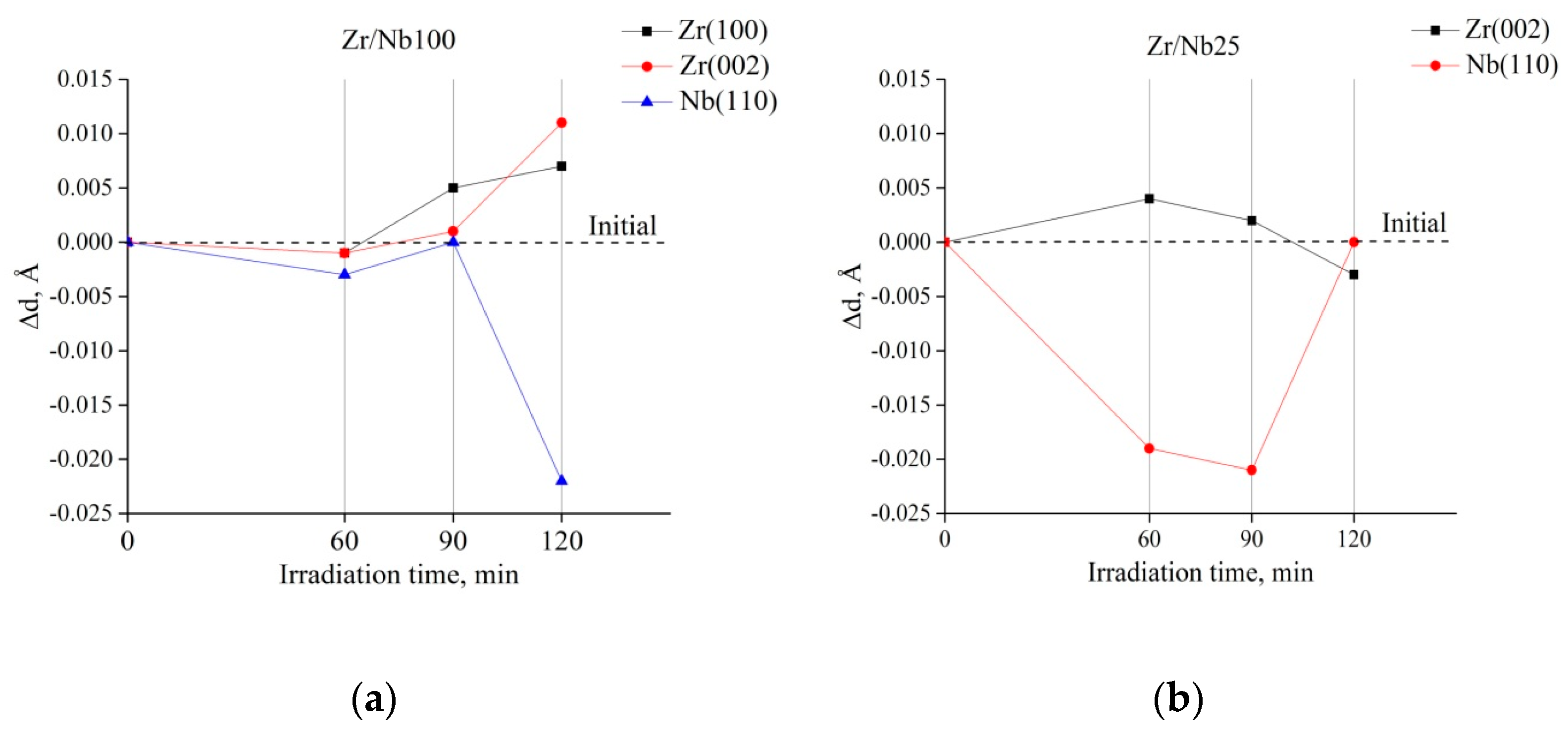
3.3. XRD Structure Analysis

The XRD investigation performed for the initial and proton-irradiated Zr/Nb100 and Zr/Nb25 NMCs revealed that Zr/Nb100 have Zr (100), Zr (002), and Nb (110) orientation: for Zr/Nb25 only Zr (002) and Nb (110) diffraction peaks were detected.
In the case of Zr/Nb100 multilayers (Figure 3a), no peak shift was observed up to 90 min of irradiation, whereas after 120 min of irradiation, diffraction peak shifts to a lower 2θ angle (for Zr) and to a higher 2θ angle (for Nb) occurred. In contrast for Zr/Nb25 multilayers (Figure 3b), Zr diffraction peaks remained stable at all irradiation times, and Nb diffraction peaks shifted remarkably to a higher 2θ angle over 90 min of irradiation. After reaching 120 min, no peak shifting was observed. The observed variations in the position of diffraction peaks indicate a change in interplanar spacing (d-spacing) and the presence of residual stresses on a scale larger than the grain size (macrostresses). The d-spacing was calculated using Bragg’s equation:
d = λ 2 s i n   θ   .
Figure 4 presents the changes in d-spacing (Δd) caused by H+ irradiation. It should be mentioned that the as-deposited Zr/Nb NMC coatings showed smaller d-spacing than the unstressed ideal crystals. In ideal unstressed crystal, d-spacing is 2.798 Å for Zr (100), 2.574 Å for Zr (002), and 2.334 Å for Nb (110). In this work, d-spacing in Zr/Nb100 NMCs was 2.735 Å for Zr (100), 2.566 Å for Zr (002), and 2.319 Å for Nb (110). In Zr/Nb25 NMCs it was 2.567 Å for Zr (002) and 2.328 Å for Nb (110). Hence, it can be seen that in all multilayers there was a presence of tensile macrostresses. It should be noted that d-spacing for Zr/Nb100 NMCs was more stable at lower irradiation times (60 min and 90 min) and considerably changed at 120 min of irradiation. Such changes are attributed to formation of tensile macrostress in the Nb layer and compressive macrostress in the Zr layer, causing their opposite shift. In contrast, d-spacing for Zr/Nb25 experienced lesser changes over 120 min of irradiation. However, it can be clearly seen that peaks corresponding to 120 min of irradiation became wider and less intensive in relation to the formation of residual stresses that vary on the scale of a grain (microstresses).
To estimate peak broadening due to changing of microstress on H+ irradiation, the relation between full width on half maxima of irradiated (FWHM) and initial (FWHM0) samples versus irradiation time was built. The analysis of peak broadening showed that for Zr/Nb100 multilayers with irradiation times of 60 min and 90 min the Zr (100) diffraction peak became broader, with a maximum at 60 min, while those of Zr (002) and Nb (110) remained stable (Figure 5a). After reaching 120 min of irradiation, both Zr diffraction peaks became narrower, and the Nb (110) diffraction peak slightly broadened. For Zr/Nb25 multilayers, changes in full width on half maxima were more intensive. As shown by Figure 5b, over 60 min and 90 min of irradiation the full width on half maxima value decreased remarkably, and slightly increased at 120 min of irradiation. From peak shifting and broadening it can be noted that Zr/Nb NMCs responded to irradiation by the formation of macro- or microstresses. NMCs that showed formation of macrostresses (Zr/Nb100: 120 min; Zr/Nb25: 60, 90 min) did not show the formation of microstresses, and vice versa. The decrease in full width on half maxima value indicates a microstress decrease in the coatings due a probable reduction of defectiveness with some kind of restoration process. This could be related to the motion of existing dislocations to the interfaces triggered by ion bombardment. This motion of existing dislocations and irradiation-induced defects with further accumulation can shear interfaces [40], causing macrostresses to occur. The appearance of macrostresses in Zr/Nb25 NMCs at shorter irradiation times is associated with a higher volume density of the interfaces; consequently, it is easier for defects to reach them. Further accumulation of damage on the interfaces may lead to non-uniform distribution of stress that appears in wide and less intensive peaks on XRD for Zr/Nb25 NMCs exposed to 120 min of irradiation.

3.4. Resistivity Measurements

It is generally known that during irradiation the electrical resistance should increase in proportion to the defect concentration, indicating the presence of a defect structure. The following equation determined the resistivity of unirradiated and irradiated Zr/Nb NMCs:
ρ = 4.53 × U I t ,
where 4.53 is the constant related to the distance between probes, U and I are probe voltage and current, respectively, and t is the coating thickness.
The dependence of resistivity on irradiation time showed that there was no increase in resistivity of the Zr/Nb NMCs after irradiation (Figure 6a,b). For Zr/Nb100 irradiated for 60 min and 120 min, decreases in resistivity of 10% and 26% were detected, respectively. For Zr/Nb25, no apparent changes in electrical resistivity were noted. Hence, the concentration of defects in the irradiated samples was the same or lower than in unirradiated ones, proving the recovery process during irradiation.

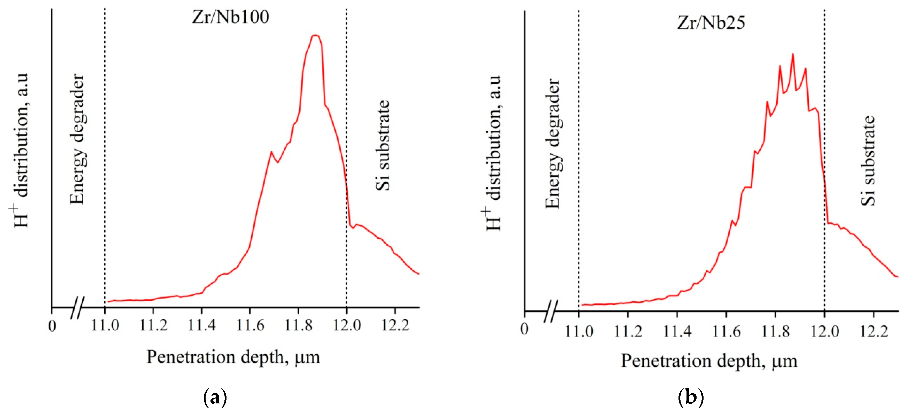
3.5. Variable Energy Positron Beam Spectroscopy

Figure 7 shows the dependence of S parameters on the energy of incident positrons for Zr/Nb100 and Zr/Nb25 after and before proton irradiation. The upper axis was calculated using Equation (4) and parameters for Nb: m = 1.733, n = 1.662, and A = 2.87 [41], taking into account different densities of Nb and Zr. The S parameter for 100 nm system firstly increased with positron energies up to 9 keV. This increase was caused by the difference in S parameter for Zr and Nb films. The S parameter was higher for Zr, and this rise is linked with the number of positrons annihilated in the Zr layer. When the energy of positrons was sufficient to reach the third layer (over 13 keV), a drop in the S parameter could be observed. The depth resolution decreased with positron energy and was caused by comprehensive implantation profile, according to Equation (3). For energies higher than 15 keV due to poor resolution, the following layers could only be described by the mean S parameter. In other words, positrons annihilate in several layers at once. It could also be seen that the S parameter increased when positrons reached the substrate Si region at about 30–32 keV. Performed studies indicated that S parameter of the initial sample decreased with irradiation time and was the lowest for samples irradiated for 120 min, especially at a depth of 800 nm corresponding to Bragg peak position (see Figure 2). This was caused by lower defect concentration than in the initial sample.
As for the dependency of S parameter in the 25 nm system, when the energy of positrons increased from 0.1 keV to 3 keV, there was a similar gradual increase in the S parameter in all samples, caused by the implantation of positrons to the second layer. The end of the second layer was blurry. The decrease in layer size made it difficult to recognize the boundary of layers. This could be for two reasons. Firstly, a depth resolution is not sufficient to observe a single 25 nm layer. Secondly, positrons can easily diffuse to the boundary of films and annihilate on its surface, causing S parameters to be almost constant over all layers. Only small increase of S parameter could be noted when positrons reached the silicon after an energy of 33 keV, similar to the Zr/Nb100. The S parameter differences for initial and irradiated samples were minimal. Additional defects were not observed. Furthermore, at a depth of around 800 nm the S parameters for irradiated and unirradiated samples were within the uncertainty range. The PAS measurements indicated that for both layer systems the defect evolution was similar and did not change much with irradiation time in the Bragg peak area. To analyze types of defects it is necessary to consider the dependence of S (W).
Figure 8 shows the dependence of the S (W) parameter for the 100 nm and 25 nm Zr/Nb NMCs. As can be seen from Figure 8a, defects arose from proton irradiation in all samples and were almost identical. The S-W points for treated samples lay on a straight line but with a lower position than initial ones. That indicates that defects type changed slightly during irradiation. More significant differences were observed for Zr/Nb25 samples (see Figure 8b). Here, in all samples the defect type drastically changed and depended on irradiation time. This suggests that with the increasing number of interfaces between coatings, the process of defect evolution depends on the dose and becomes more complicated.

3.6. Investigation of NMCs Zr/Nb by Beam Positron Spectroscopy and GD–OES

When analyzing coatings by the GD-OES method, a layer-by-layer correlation of data with beam positron spectroscopy was discovered, which led us to consider these results in more detail. Figure 9 shows graphs of the dependence of the Zr and Nb emission intensity on the sputtering depth of the initial sample with a coating of 100 ± 10 nm and the relationship of the positron energy with the S parameter of the initial and irradiated samples. The results obtained by GD–OES were in good agreement with the results of the positron beam spectroscopy. One can note a certain tendency: during the sputtering of the niobium layer, the S parameter increased, and during the sputtering of the zirconium layer, the S parameter decreased. Furthermore, this cycle was repeated throughout the entire measurement range; this behavior of the S parameter was caused by different lattices of these metals. Hence, peaks and drops began at the layer interface, as confirmed by the results of GD–OES.
Figure 10 shows dependence of the Zr and Nb emission intensity on the sputtering depth of the initial sample with a coating of 25 ± 2 nm and the relevance of positron energy on the S parameter of the initial and irradiated samples. In this case, the cycle was repeated over the entire measurement range as in the graphs above; this behavior of the S parameter is also explained by different lattices of the studied metals.
Therefore, when analyzing multilayer coatings based on Zr and Nb, it can be assumed that the defective structure of these NMCs does not increase upon proton irradiation; the interfaces do not mix either before or after irradiation.

4. Conclusions

The Zr/Nb-based NMCs with thicknesses of individual layers of 100 ± 10 nm and 25 ± 2 nm were successfully deposited by DC magnetron sputtering. The obtained NMCs were irradiated with 900 keV protons for various times periods (60 min to 120 min). As a result of the work, the following conclusions can be drawn:
(1)
The study of the distribution of layers and chemical elements of Zr/Nb NMCs using GD–OES before and after irradiation with 900 keV photons with different irradiation duration times from 60 min to 120 min showed that the structure of the NMCs did not change as a result of irradiation, and the layers did not mix;
(2)
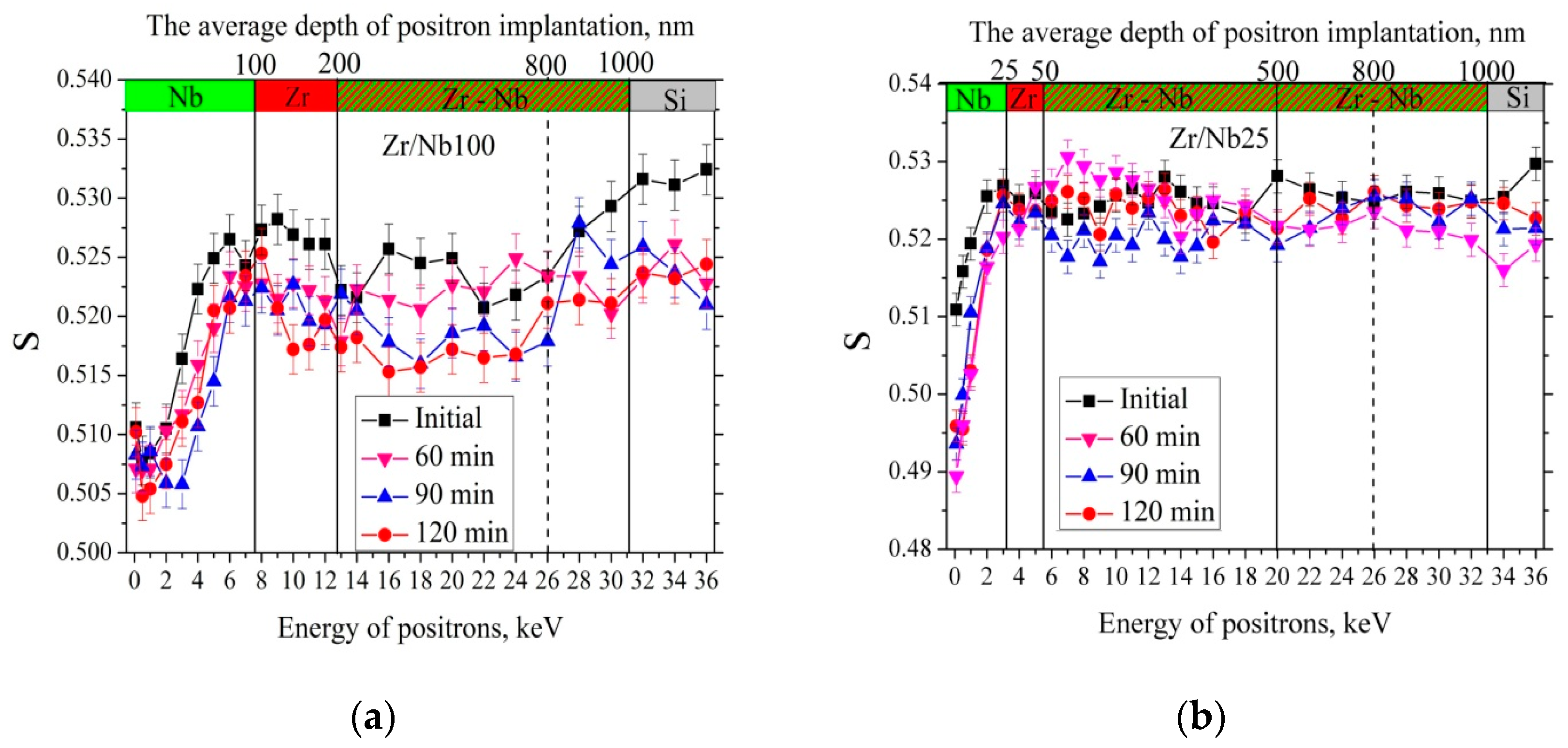
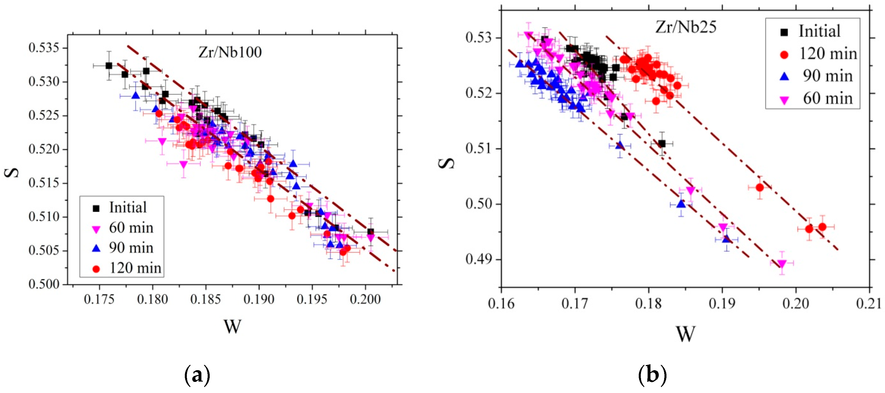
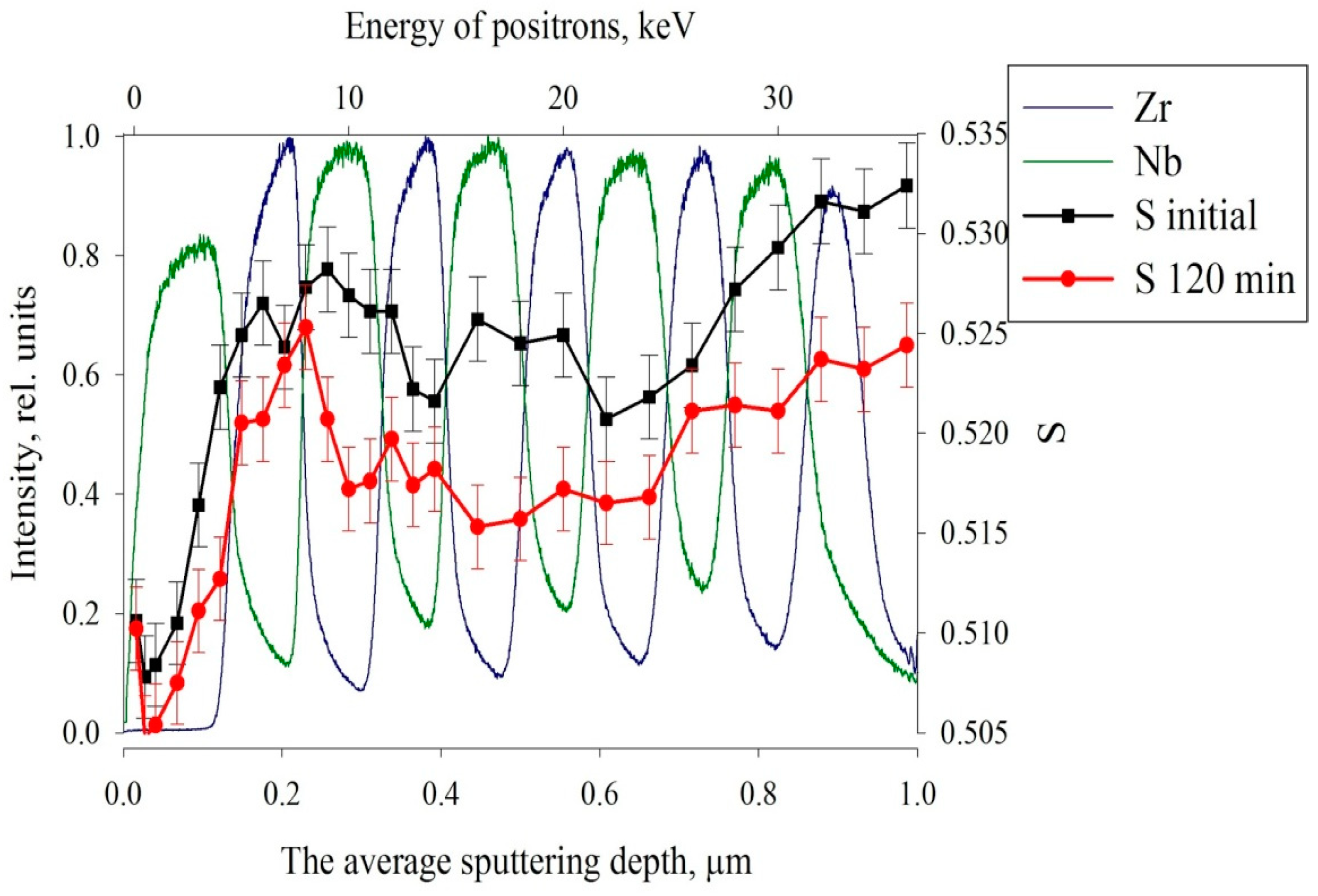
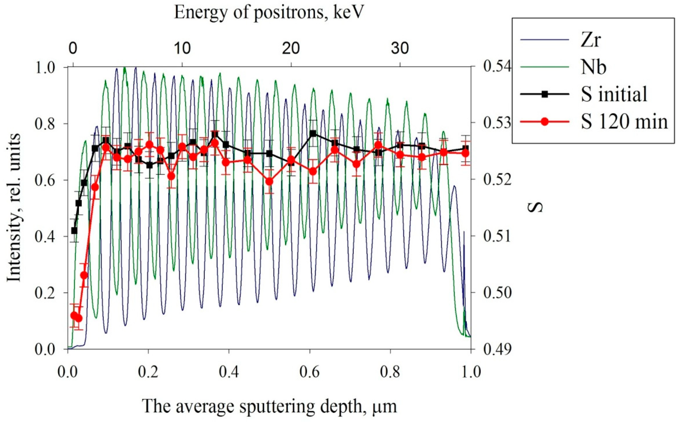
A study of the distribution of defects in Zr/Nb NMCs before and after irradiation with protons using positron beams with variable energy by Doppler broadening spectroscopy method showed that the defect structure of the samples before and after irradiation was approximately on the same level; in some cases at a depth around 800 nm corresponding to Bragg peak there was a slight decrease in defectiveness in irradiated samples;
(3)
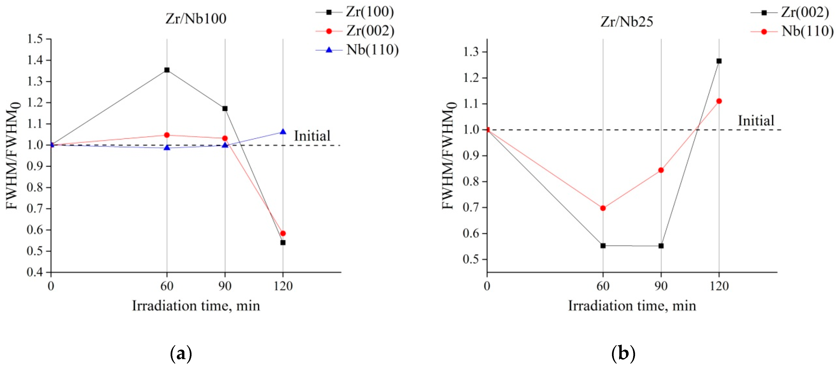
Microstructure evolution of Zr/Nb NMCs after irradiation examined by XRD study showed good radiation tolerance against 900 keV H+ irradiation. However, detected some minor changes were detected in diffraction peak positions and full width on half maxima values. Zr/Nb25 showed higher sensitivity to doses at 60 min and 90 min of irradiation, and Zr/Nb100 was more sensitive to doses at 120 min;
(4)
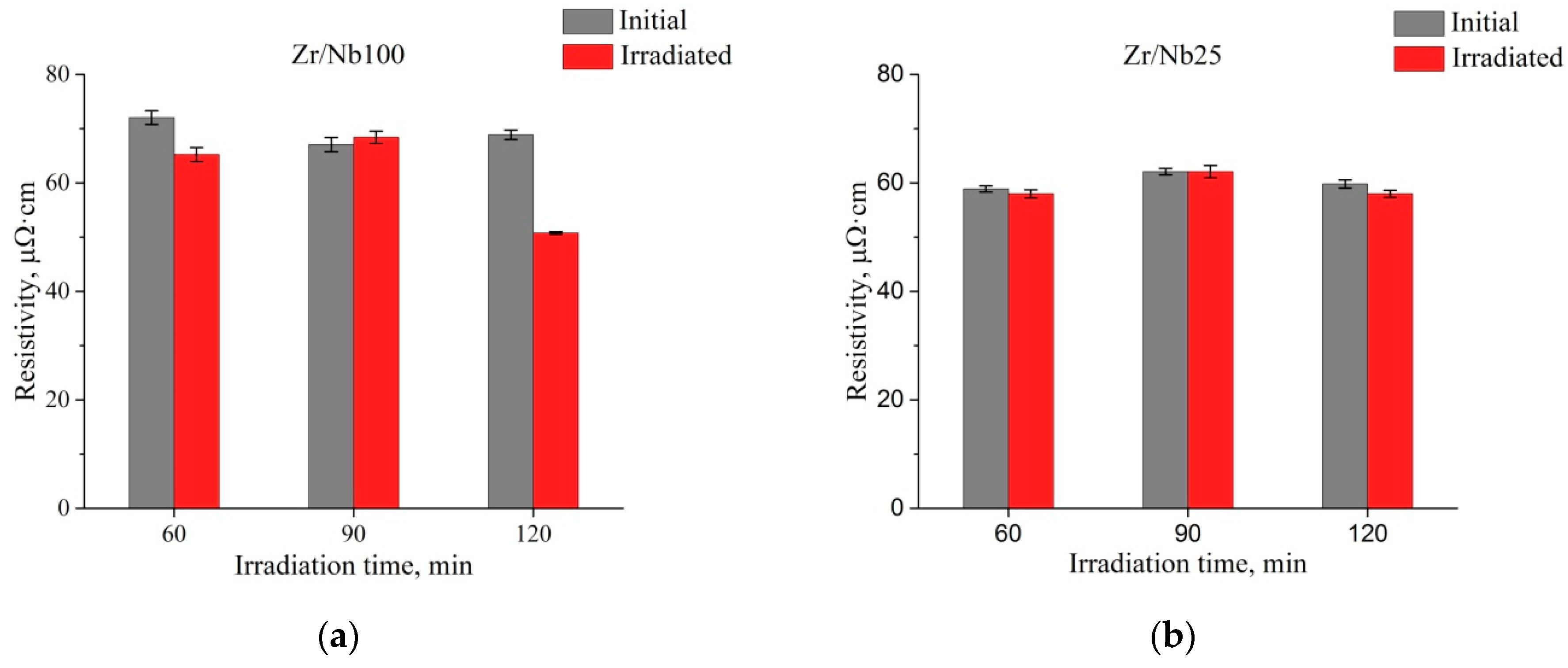
Investigation of electrical resistance showed nearly zero changes of resistivity after irradiation for most regimes. For Zr/Nb100 irradiated during 60 min and 90 min decreases in resistivity of 10% and 26%, respectively, were observed;
(5)
Studies showed that irradiation of Zr/Nb NMCs with H+ did not lead to any severe damage and in some cases the structure of the coatings became more ordered than in the native ones. This phenomenon can be attributed to the fact that at such doses, the defect formation rate is suppressed by the high volume density of defect sinks and is not sufficient for the formation of a stable defective structure. Moreover, the macrostresses on the interfaces occurring during irradiation stimulate the diffusion mobility of defects, leading to the reduction of the overall defect level.

Author Contributions

R.L. organized the workflow and preparation of the article. A.L. measured samples using the GD–OES method. D.K. provided SRIM calculations and irradiation of the samples. M.S. performed XRD analysis. E.K. carried out sample preparation and microstructure analysis using electron microscopy methods. Y.B. measured and analyzed electrical resistances. K.S. and A.K. performed adjustment and layer-by-layer analysis using positron spectroscopy methods. All authors read and agreed to the published version of the manuscript.

Funding

This work was carried out within the framework of the Competitiveness Enhancement Program of National Research Tomsk Polytechnic University.

Acknowledgments

The authors are grateful to TPU associate professor Dmitrii Sidelev for the help in preparing samples and discussing the results as well as Aleksei Obrosov for SEM measurements.

Conflicts of Interest

The authors declare no conflict of interest.

References

  1. Uglov, V.V.; Abadias, G.; Zlotski, S.V.; Kvasov, N.T.; Saladukhin, I.A.; Malashevih, A.A. Blister formation in ZrN/SiN multilayers after He irradiation. Surf. Coat. Technol. 2018, 344, 170–176. [Google Scholar] [CrossRef]
  2. Abadias, G.; Uglov, V.V.; Saladukhin, I.A.; Zlotski, S.V.; Tolmachova, G.; Dub, S.N.; van Vuuren, A.J. Growth, structural and mechanical properties of magnetron-sputtered ZrN/SiNx nanolaminated coatings. Surf. Coat. Technol. 2016, 308, 158–167. [Google Scholar] [CrossRef]
  3. Callisti, M.; Karlik, M.; Polcar, T. Competing mechanisms on the strength of ion-irradiated Zr/Nb nanoscale multilayers: Interface strength versus radiation hardening. Scr. Mater. 2018, 152, 31–35. [Google Scholar] [CrossRef] [Green Version]
  4. Ryskulov, A.E.; Kozlovskiy, A.L.; Ivanov, I.A.; Uglov, V.V.; Kislitsin, S.B.; Zdorovets, M.V. The effect of Ni12+ heavy ion irradiation on the optical and structural properties of BeO ceramics. Ceram. Int. 2020, 46, 4065–4070. [Google Scholar] [CrossRef]
  5. Uglov, V.V.; Abadias, G.; Zlotski, S.V.; Saladukhin, I.A.; Safronov, I.V.; Shymanski, V.I.; Janse van Vuuren, A.; O’Connell, J.; Skuratov, V.; Neethling, J.H. Features of microstructure of ZrN, Si3N4 and ZrN/SiNx nanoscale films irradiated by Xe ions. Vacuum 2017, 143, 491–494. [Google Scholar] [CrossRef]
  6. Sen, H.S.; Polcar, T. Vacancy-interface-helium interaction in Zr-Nb multi-layer system: A first-principles study. J. Nucl. Mater. 2019, 518, 11–20. [Google Scholar] [CrossRef]
  7. Callisti, M.; Lozano-Perez, S.; Polcar, T. Structural and mechanical properties of γ-irradiated Zr/Nb multilayer nanocomposites. Mater. Lett. 2016, 163, 138–141. [Google Scholar] [CrossRef] [Green Version]
  8. Ham, B.; Zhang, X. High strength Mg/Nb nanolayer composites. Mater. Sci. Eng. A 2011, 528, 2028–2033. [Google Scholar] [CrossRef]
  9. Yang, G.H.; Zhao, B.; Gao, Y.; Pan, F. Investigation of nanoindentation on Co/Mo multilayers by the continuous stiffness measurement technique. Surf. Coat. Technol. 2005, 191, 127–133. [Google Scholar] [CrossRef]
  10. Lu, Y.Y.; Kotoka, R.; Ligda, J.P.; Cao, B.B.; Yarmolenko, S.N.; Schuster, B.E.; Wei, Q. The microstructure and mechanical behavior of Mg/Ti multilayers as a function of individual layer thickness. Acta Mater. 2014, 63, 216–231. [Google Scholar] [CrossRef]
  11. Zhang, J.Y.; Lei, S.; Liu, Y.; Niu, J.J.; Chen, Y.; Liu, G.; Zhang, X.; Sun, J. Length scale-dependent deformation behavior of nanolayered Cu/Zr micropillars. Acta Mater. 2012, 60, 1610–1622. [Google Scholar] [CrossRef]
  12. Demkowicz, M.J.; Wang, Y.Q.; Hoagland, R.G.; Anderoglu, O. Mechanisms of he escape during implantation in CuNb multilayer composites. Nucl. Instrum. Methods Phys. Res. Sect. B Beam Interact. Mater. Atoms 2007, 261, 524–528. [Google Scholar] [CrossRef]
  13. Wei, Q.M.; Li, N.; Mara, N.; Nastasi, M.; Misra, A. Suppression of irradiation hardening in nanoscale V/Ag multilayers. Acta Mater. 2011, 59, 6331–6340. [Google Scholar] [CrossRef]
  14. Gao, Y.; Yang, T.; Xue, J.; Yan, S.; Zhou, S.; Wang, Y.; Kwok, D.T.K.; Chu, P.K.; Zhang, Y. Radiation tolerance of Cu/W multilayered nanocomposites. J. Nucl. Mater. 2011, 413, 11–15. [Google Scholar] [CrossRef]
  15. Chen, F.; Tang, X.; Yang, Y.; Huang, H.; Chen, D. Investigation of structural stability and magnetic properties of Fe/Ni multilayers irradiated by 300 keV Fe10+. J. Nucl. Mater. 2014, 452, 31–36. [Google Scholar] [CrossRef]
  16. Mastorakos, I.N.; Zbib, H.M.; Bahr, D.F. Deformation mechanisms and strength in nanoscale multilayer metallic composites with coherent and incoherent interfaces. Appl. Phys. Lett. 2009, 94, 173114. [Google Scholar] [CrossRef]
  17. Frutos, E.; Callisti, M.; Karlik, M.; Polcar, T. Length-scale-dependent mechanical behaviour of Zr/Nb multilayers as a function of individual layer thickness. Mater. Sci. Eng. A 2015, 632, 137–146. [Google Scholar] [CrossRef]
  18. Monclús, M.A.; Callisti, M.; Polcar, T.; Yang, L.W.; Llorca, J.; Molina-Aldareguía, J.M. Selective oxidation-induced strengthening of Zr/Nb nanoscale multilayers. Acta Mater. 2017, 122, 1–10. [Google Scholar] [CrossRef] [Green Version]
  19. Callisti, M.; Polcar, T. Combined size and texture-dependent deformation and strengthening mechanisms in Zr/Nb nano-multilayers. Acta Mater. 2017, 124, 247–260. [Google Scholar] [CrossRef] [Green Version]
  20. Lei, S.; Zhang, J.Y.; Niu, J.J.; Liu, G.; Zhang, X.; Sun, J. Intrinsic size-controlled strain hardening behavior of nanolayered Cu/Zr micropillars. Scr. Mater. 2012, 66, 706–709. [Google Scholar] [CrossRef]
  21. Yang, W.; Pang, J.; Zheng, S.; Wang, J.; Zhang, X.; Ma, X. Interface Effects on He Ion Irradiation in Nanostructured Materials. Materials 2019, 12, 2639. [Google Scholar] [CrossRef] [PubMed] [Green Version]
  22. Čížek, J. Characterization of lattice defects in metallic materials by positron annihilation spectroscopy: A review. J. Mater. Sci. Technol. 2018, 34, 577–598. [Google Scholar] [CrossRef]
  23. Triftshäuser, W.; Kögel, G.; Sperr, P. Characterization of Radiation-Induced Defects in ZnO Probed by Positron Annihilation Spectroscopy. Mater. Sci. Forum 2001, 363–365, 141–143. [Google Scholar]
  24. Ogorodnikova, O.V.; Dubov, L.Y.; Stepanov, S.V.; Terentyev, D.; Funtikov, Y.V.; Shtotsky, Y.V.; Stolbunov, V.S.; Efimov, V.; Gutorov, K. Annealing of radiation-induced defects in tungsten: Positron annihilation spectroscopy study. J. Nucl. Mater. 2019, 517, 148–151. [Google Scholar] [CrossRef]
  25. Shpotyuk, O.; Filipecki, J. Radiation-induced defects in vitreous chalcogenide semiconductors studied by positron annihilation method. Mater. Sci. Eng. B Solid-State Mater. Adv. Technol. 2002, 91–92, 537–540. [Google Scholar] [CrossRef]
  26. Cao, G.R.; Guo, S.K.; Wang, Z.C.; Teng, M.K.; Chen, C.; Liu, Y.C. Induced defects in a-Si:H/a-SiNx:H multilayers by use of a positron annihilation technique. Mod. Phys. Lett. B 1996, 10, 1–10. [Google Scholar] [CrossRef]
  27. Parente, P.; Ortega, Y.; Savoini, B.; Monge, M.A.; Tucci, A.; Esposito, L.; Ferrari, B.; Sanchez-Herencia, A.J. Characterization of residual compressive stresses in layered ceramics by positron annihilation spectroscopy. J. Eur. Ceram. Soc. 2012, 32, 3989–3993. [Google Scholar] [CrossRef] [Green Version]
  28. Duarte Naia, M.; Gordo, P.M.; Teodoro, O.M.N.D.; De Lima, A.P.; Moutinho, A.M.C. Characterisation of Ti/Al Multilayered Structures with Slow Positron Beams Applying a Simplified Positron Depth Distribution Model. Mater. Sci. Forum 2010, 636–637, 1097–1101. [Google Scholar] [CrossRef]
  29. Gregory, R.B.; Su, W. Monte Carlo calculation of positron implantation in multilayered materials. Nucl. Inst. Methods Phys. Res. B 1991, 62, 1–7. [Google Scholar] [CrossRef]
  30. Sidelev, D.V.; Yurjev, Y.N.; Krivobokov, V.P.; Erofeev, E.V.; Penkova, O.V.; Novikov, V.A. The oxygen-deficient TiO2 films deposited by a dual magnetron sputtering. Vacuum 2016, 134, 29–32. [Google Scholar] [CrossRef]
  31. Zaitcev, D.; Sidelev, D.; Tupikova, O. Effect of magnetic field configuration of dual magnetron on carbon based films properties. Adv. Mater. Res. 2014, 1040, 721–725. [Google Scholar]
  32. Syrtanov, M.; Garanin, G.; Kashkarov, E.; Pushilina, N.; Kudiiarov, V.; Murashkina, T. Laboratory X-ray Diffraction Complex for In Situ Investigations of Structural Phase Evolution of Materials under Gaseous Atmosphere. Metals 2020, 10, 447. [Google Scholar] [CrossRef] [Green Version]
  33. Priamushko, T.; Mikhaylov, A.; Babikhina, M.; Kudiiarov, V.; Laptev, R. Glow Discharge Optical Emission Spectrometer Calibration Using Hydrogenated Zr-2.5Nb Alloy Standard Samples. Metals 2018, 8, 372. [Google Scholar] [CrossRef] [Green Version]
  34. Mikhaylov, A.A.; Priamushko, T.S.; Babikhina, M.N.; Kudiiarov, V.N.; Heller, R.; Laptev, R.S.; Lider, A.M. Hydrogen calibration of GD-spectrometer using Zr-1Nb alloy. Appl. Surf. Sci. 2018, 432, 85–89. [Google Scholar] [CrossRef]
  35. Bordulev, Y.S.; Laptev, R.S.; Kudiiarov, V.N.; Lider, A.M. Investigation of commercially pure titanium structure during accumulation and release of hydrogen by means of positron lifetime and electrical resistivity measurements. Adv. Mater. Res. 2014, 880, 93–100. [Google Scholar] [CrossRef]
  36. Horodek, P.; Kobets, A.G.; Meshkov, I.N.; Sidorin, A.A.; Orlov, O.S. Slow positron beam at the JINR, Dubna. Nukleonika 2015, 60, 725–728. [Google Scholar] [CrossRef] [Green Version]
  37. Horodek, P.; Bugdol, M.; Kobets, A.G.; Meshkov, I.N.; Orlov, O.S.; Rudakov, A.Y.; Sidorin, A.A.; Yakovenko, S.L. Development of positron annihilation spectroscopy at LEPTA facility. Phys. Part. Nucl. Lett. 2014, 11, 708–712. [Google Scholar] [CrossRef] [Green Version]
  38. Dryzek, J.; Horodek, P. Positron implantation profiles in layered samples. Nucl. Instrum. Methods Phys. Res. Sect. B Beam Interact. Mater. Atoms 2009, 267, 3580–3589. [Google Scholar] [CrossRef]
  39. Ziegler, J.F.; Ziegler, M.D.; Biersack, J.P. SRIM—The stopping and range of ions in matter (2010). Nucl. Instrum. Methods Phys. Res. Sect. B Beam Interact. Mater. Atoms 2010, 268, 1818–1823. [Google Scholar] [CrossRef] [Green Version]
  40. Zbib, H.M.; Overman, C.T.; Akasheh, F.; Bahr, D. Analysis of plastic deformation in nanoscale metallic multilayers with coherent and incoherent interfaces. Int. J. Plast. 2011, 27, 1618–1639. [Google Scholar] [CrossRef]
  41. Dryzek, J.; Horodek, P. GEANT4 simulation of slow positron beam implantation profiles. Nucl. Instrum. Methods Phys. Res. Sect. B Beam Interact. Mater. Atoms 2008, 266, 4000–4009. [Google Scholar] [CrossRef]
Figure 1. Cross-section SEM images of the as-deposited Zr/Nb nanoscale multilayer coatings (NMCs): 25/25 nm (a) and 100/100 nm (b).
Metals 10 00535 g001
Figure 2. Distribution versus penetration depth of a 900-keV proton beam for Zr/Nb100 (a) and Zr/Nb25 (b) simulated in SRIM-2013. Zr/Nb25: Zr/Nb coatings with a layer periodicity of 25 nm; Zr/Nb100: Zr/Nb coatings with layer periodicity of 100 nm.
Metals 10 00535 g002
Figure 3. XRD patterns for the initial and proton-irradiated Zr/Nb100 (a) and Zr/Nb25 (b) multilayers.
Metals 10 00535 g003
Figure 4. D-spacing evolution due to H+ irradiation of Zr/Nb100 (a) and Zr/Nb25 (b) NMCs.
Metals 10 00535 g004
Figure 5. Relation of full width on half maxima of irradiated (FWHM) and initial (FWHM0) sample values for specific diffraction peaks due to H+ irradiation for Zr/Nb100 (a) and Zr/Nb25 (b) NMCs.
Metals 10 00535 g005
Figure 6. Resistivity versus irradiation time for Zr/Nb100 (a) and Zr/Nb25 (b) NMCs.
Metals 10 00535 g006
Figure 7. Depth profile of the S parameter for Zr/Nb100 (a) and Zr/Nb25 (b).
Metals 10 00535 g007
Figure 8. Dependence of the S = f(W) parameter for irradiated and initial Zr/Nb100 (a) and Zr/Nb25 (b) samples.
Metals 10 00535 g008
Figure 9. Depth distribution profile for the Zr and Nb elements and the S parameter for Zr/Nb100.
Metals 10 00535 g009
Figure 10. Depth distribution profile for the elements Zr and Nb and the S parameter for Zr/Nb25.
Metals 10 00535 g010

