Article

Analysing Efficiency and Reliability of High Speed Drive Inverters Using Wide Band Gap Power Devices

Institute for Electrical Machines, Traction and Drives (IMAB), TU Braunschweig, 38106 Braunschweig, Germany
*
Author to whom correspondence should be addressed.
Machines 2021, 9(12), 350; https://doi.org/10.3390/machines9120350
Submission received: 22 October 2021 / Revised: 3 December 2021 / Accepted: 7 December 2021 / Published: 9 December 2021
(This article belongs to the Special Issue High Speed Air Compressor for a Fuel Cell System for Use in a Vehicle)

Abstract

:
Within the project ‘ARIEL’ an electrical turbo compressor unit for fuel cell applications is deeply investigated. The necessary drive inverter is especially designed for high fundamental frequency and high switching frequency to cope with the requirements of the implemented electrical machine. This paper presents investigations on the inverter’s efficiency and its prospective lifetime at different stages of the development. In the design process different wide band gap power semiconductor devices in discrete packages are evaluated in terms of the achievable power density and efficiency, both by simulations and measurements. Finally, an optimised design using surface mount silicon carbide MOSFETs is developed. Compared to a former inverter design using silicon devices in a three-level topology, the power density of the inverter is significantly increased. The lifetime of power electronic systems is often limited by the lifetime of the power semiconductor devices. Based on loss calculations and the resulting temperature swing of the virtual junction the lifetime of the inverter is estimated for the most frequent operating points and for different mission profiles.

1. Introduction

This article describes the research and development that is performed in the field of power electronics during the funded collaborative project ‘ARIEL’. The main goal is the development of a drive inverter with special requirements in terms of switching frequency with a high power density, high efficiency and good reliability.
The target application is the electrical turbo compressor unit of an automotive fuel cell system. The high performance and high-speed electrical machine used in this application strictly defines some challenging requirements that are addressed by the presented investigations.
Figure 1 illustrates the performed design process and also represents the structure of this article. In a first part, the design of possible drive inverter implementations is described. Step by step, the requirements are collected, and possible solutions are defined. These are compared and evaluated based on theoretical analysis and power loss simulations. Afterwards, the most promising solutions are compared with each other based on the practical evaluation of power stage prototypes in a test bench. The execution and the results of these extensive measurements are described in detail in the second part of the article.
In parallel to this design process, the expected lifetime of different power semiconductor devices is determined. Therefore, the third section deals with a method for lifetime estimation of power electronics. A selection of wide band gap semiconductors is investigated for different operating points and different mission profiles.

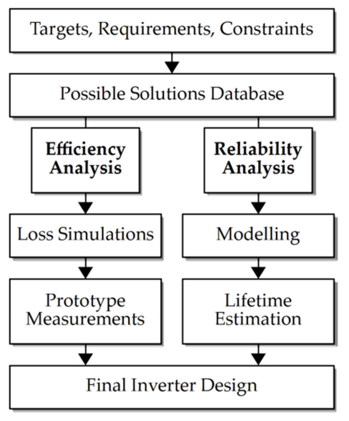
2. Drive Inverter Design Procedure

The development and design of the specific electrical machine used in the target application is described in [1]. High speed permanent magnet synchronous machines with surface mount or solid magnets and small stator inductance are especially sensitive against higher frequency harmonic currents that cause additional losses [2,3,4,5,6]. This can be addressed by either multi-level inverter topologies or high switching frequencies [7,8]. To reach higher switching frequencies, wide band gap power devices with low switching losses can be utilised [9,10,11,12,13]. Many different devices based on silicon carbide (SiC) and gallium nitride (GaN) substrates are already available and [14,15,16,17] specifically focus on the use of GaN devices for high-speed drive applications.
After defining targets, requirements and constraints for the new design, a wide range of different possible inverter designs including two-level and three-level topologies using silicon, SiC and GaN devices is defined and compared within this project. Preliminary results are also published in [18,19,20] and are summarised in this section. Based on a theoretical evaluation and loss simulations, a selection of different wide band gap inverters is realised and operated in an inverter test bench. The results are shown in the next section.

2.1. Definition of Targets, Requirements and Constraints

In the first step of the design procedure, the most important targets, requirements and constraints are collected and evaluated. These arise from the general application, the specific motor design and the automotive background.
The drive system is supposed to operate from a DC power system with a voltage ranging from 250 V up to 500 V. The nominal power is defined as 15 kW with some safety margin. A liquid cooling system may be used. The main design targets are high efficiency as well as high power density.
The electrical machine integrated in the turbo-compressor-unit is a synchronous machine with a solid two-pole permanent magnet rotor. The electrical fundamental frequency is 2000 Hz at a mechanical speed of 120,000 rpm. The inductance of the machine’s stator winding is small and the permanent magnet rotor is sensitive against harmonic content in the stator current. Since the permanent magnet cannot be segmented to reduce eddy currents due to mechanical reasons, and it cannot be cooled very efficiently, a high switching frequency of the drive inverter is mandatory to keep the ripple current as small as possible. Figure 2 shows predicted rotor losses as a function of the inverter’s switching frequency. A minimum switching frequency of 60 kHz is selected. Nevertheless, a switching frequency of up to 120 kHz would further reduce the rotor losses and is the target of the following investigations. Table 1 summarises the collected requirements.
For the performance analysis, three important operating points (OP) are defined. Representing the most typical steady state operation, OP (1) is defined at a load current of 30 Arms and a high modulation index of 0.9. The highest efficiency is targeted for these conditions. OP (2) describes the static full load operation at 42 Arms. This is the crucial operation for the thermal design and defines the maximum static thermal resistance of the cooling system. Finally, OP (3) represents the dynamic operation at the highest torque needed for rapid acceleration of the motor’s shaft. The most important values for these three operating points are listed in Table 2.

2.2. Theoretical Analysis and Loss Estimation

According to the defined requirements a large variety of possible solutions in terms of inverter circuit topology, power semiconductor technology and device packaging is defined. For the required voltage and power range, conventional two-level inverters (see Figure 3) or three-level designs either in NPC (neutral point clamped) I-type or T-type (see Figure 4) configuration can be selected. The current rating can be met using silicon IGBT (insulated gate bipolar transistor), silicon carbide MOSFET (metal oxide semiconductor field effect transistor) or gallium nitride devices. Especially with regard to the high switching speed demand, a strong focus is on wide band gap power devices. For all technologies, different devices with various packaging options are available, ranging from fully integrated six-pack power modules to discrete single devices in leaded or surface mount packages.
These very different solutions are compared and evaluated according to different criteria. One very important aspect is the expected efficiency. This is calculated using a loss estimation method developed especially for the flexible and fair comparison of different power semiconductor device technologies and large parameter studies on semiconductor losses. This novel calculation method is published in [21]. It is based on an analytical description of the different terms of the power devices’ losses. The medium losses in a single operating point are then calculated using numerical integration. This allows a very flexible description of different power devices and operating strategies in a consistent environment and with short calculation times.
Figure 5 shows a small selection of the obtained results. The estimated power losses of some two-level voltage source inverter designs using different wide band gap power semiconductor devices are presented, taking into account the three operating points OP (1) to OP (3) defined in Table 2. For the solutions using discrete devices, two devices are always connected in parallel to meet the load current requirements.
It can be recognised that all selected wide band gap solutions can reduce the resulting power losses compared to a three-level inverter design using silicon based IGBT technology. At a switching frequency of 60 kHz the investigated silicon carbide devices show the best performance thanks to low conduction and switching losses. For operation at up to 120 kHz GaN devices have advantages due to their even lower switching losses.
The key findings from the theoretical analysis and the loss predictions are:
  • The requirements can be met with very different solutions.
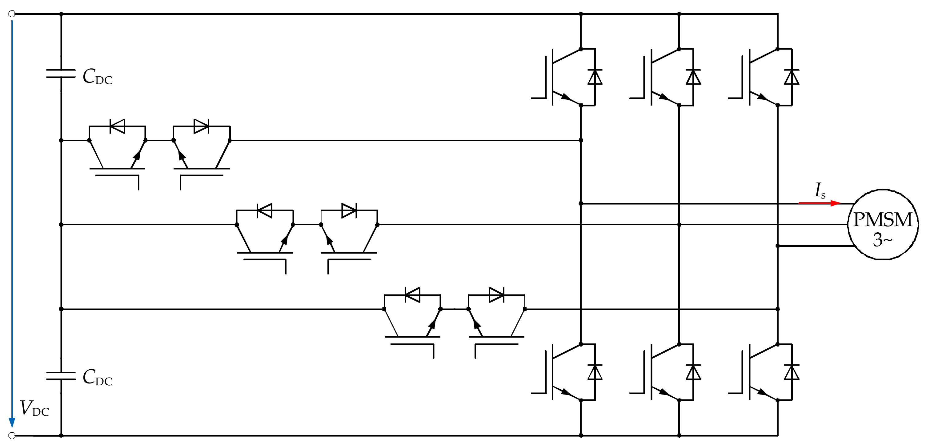
  • Silicon IGBT devices have to be used in a three-level circuit topology, since they cannot be operated at 60 kHz efficiently.
  • Using wide band gap devices, the requirements can be met with a simple two-level topology, which gives a large potential for increased power density.
  • Although the switching frequency needs to be high, high efficiency can be reached.

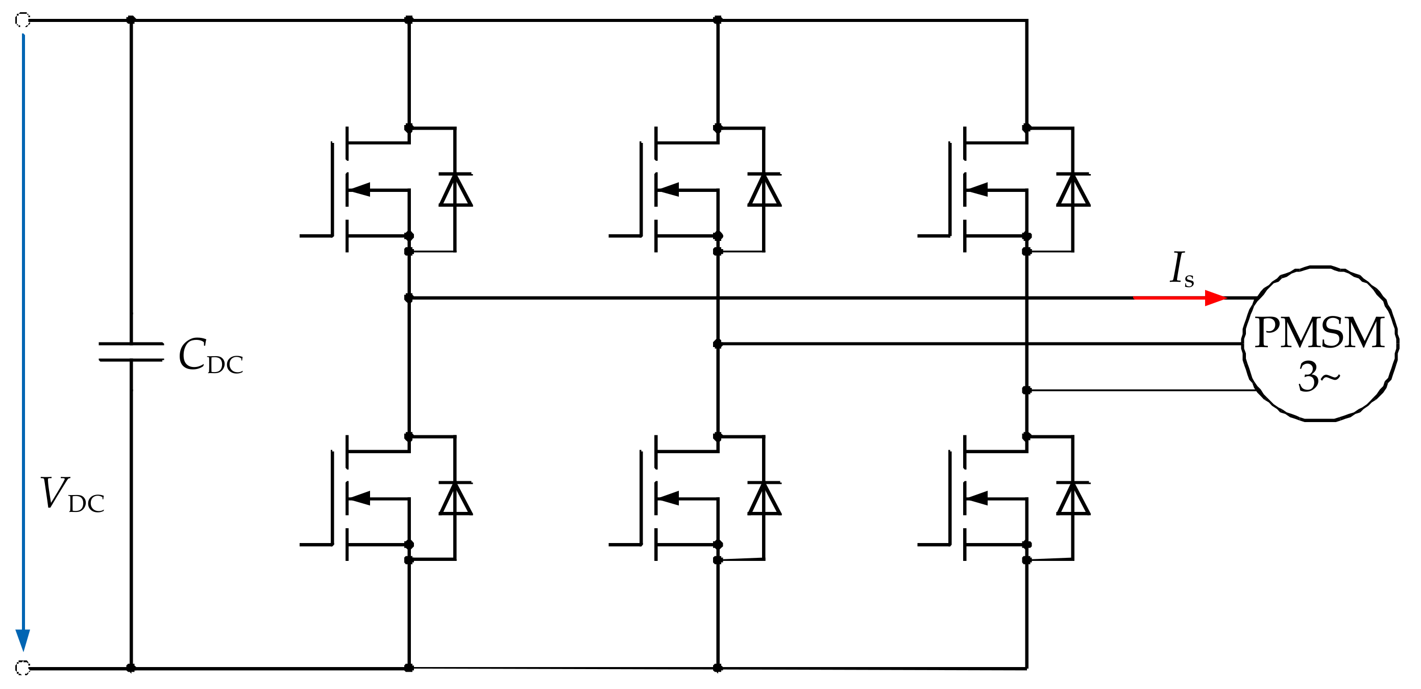
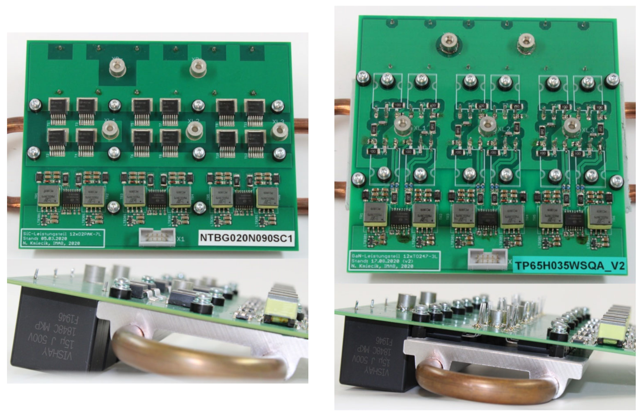
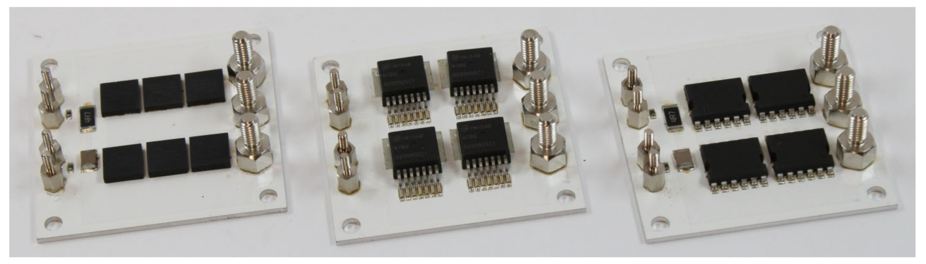
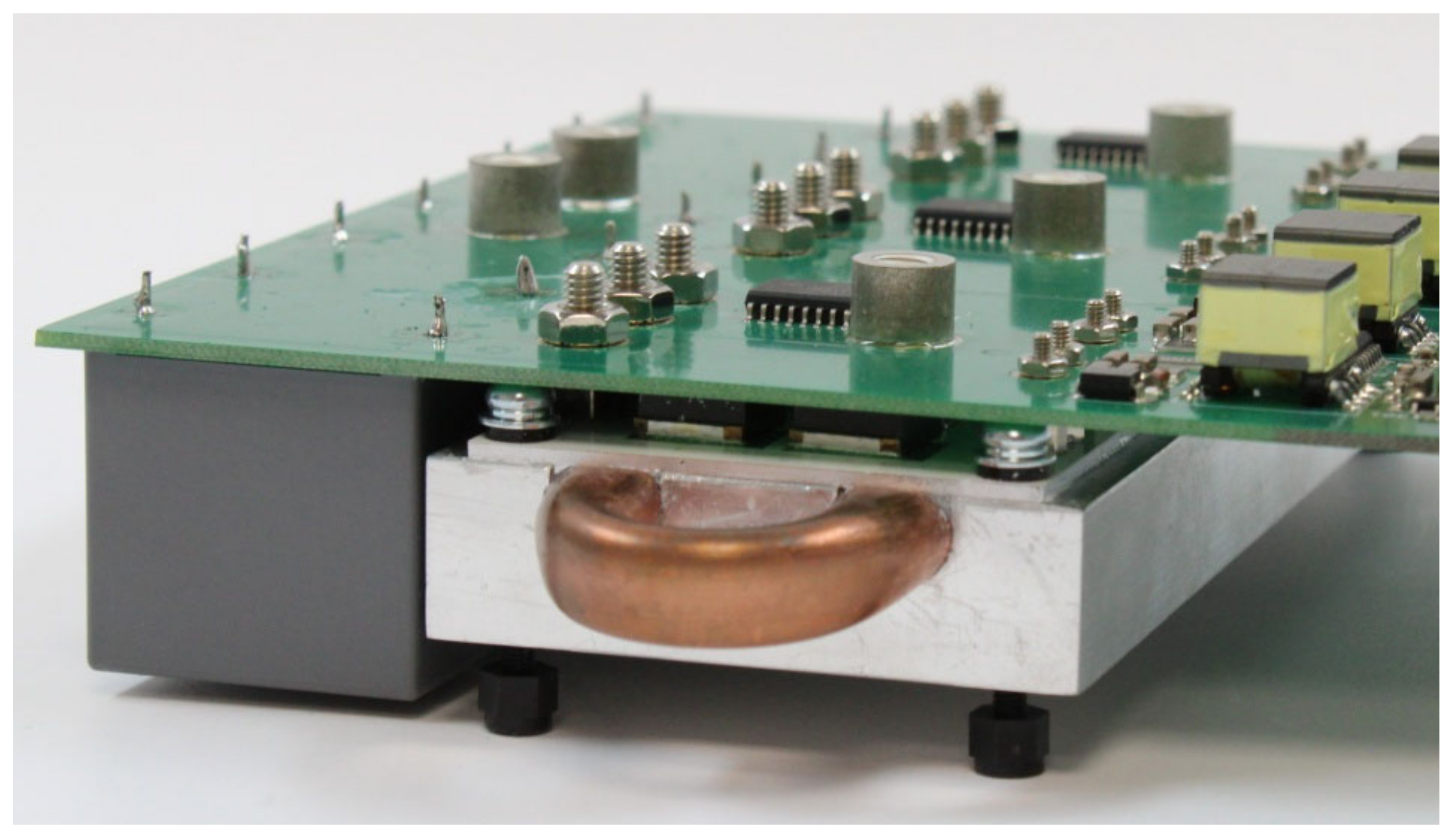
2.3. Design of Power Stage Prototypes

For a practical evaluation of different discrete power devices and a metrological validation of the loss calculation algorithm inverter, power stage prototypes are designed, built and set into operation in a test bench.
Drive inverter power stage prototypes are designed, built and set into operation in a test bench for a practical evaluation of different discrete power devices and a metrological validation of the loss calculation algorithm. The used components, the design and especially the PCB layouts are kept as similar as possible for the different power devices to have the best possible comparability. Therefore, the main differences between the individual prototypes can be found in the PCB layout in the direct environment of the power devices, the integration of different device packages and the thermal connection to the cold plate.
Figure 6 shows two of the prototypes, one using surface mount devices (D²PAK), the other using through hole devices (TO-247). On both prototypes, two devices are connected in parallel for each switch position resulting in a total number of 12 discrete devices per inverter. The easy manufacturing process using surface mount devices comes with some challenges in terms of thermal management, since the device must be cooled through the PCB. This is to be optimised not only for its electrical properties like its low inductance commutation loop and small parasitic capacitances at the load terminals but also for its low thermal resistance from the power devices on top of the PCB to the cold plate on its bottom.
In general, wide band gap devices show fast switching behaviour and steep voltage gradients. This is advantageous in terms of switching losses but can be critical in terms of electromagnetic interferences (EMI). To avoid self-EMI issues the gate drivers and their power supplies are especially designed for a high common mode rejection rate (CMR). For future application, EMI and voltage overshoot at the motor terminals are not expected to be a major issue, since the drive inverter will be integrated very closely to the electrical machine with a completely closed aluminium housing. Therefore, the conducted EMI on the DC power system feeding the inverter is the only challenge to be addressed in a future investigation.

2.4. Thermal Optimisation

During a thermal optimisation process, two different designs using surface mount power devices are developed and compared with a conventional design using TO-247 devices. The initial PCB design for D²PAK devices uses a FR4 based PCB with eight layers of copper, 70 µm each. The area under the tab of the power devices and the nearby surroundings is completely filled with an optimised pattern of thermal vias according to IPC 4761 type VII “filled and capped”. This means the vias are filled with a special epoxy plugging and capped with copper to increase the thermal conductivity. The complete board is mounted to a liquid cold plate and electrically isolated using an appropriate thermal interface material (TIM). An evenly distributed mechanical pressure on the PCB and the TIM is of high importance for this kind of construction.
The resulting total thermal resistance Rth for every single device between the junction and coolant is calculated to be about 2.9 K/W. Different measurements show a slightly higher value of about 3.3 K/W, which is about twice the thermal resistance of a TO-247 device directly mounted to the same cold plate using the same TIM.
For the second design using D²PAK surface mount power devices, an integrated metal substrate (IMS) PCB is used. It consists of a massive 1.5 mm aluminium core, a thin organic insulator with high thermal conductivity and a single structured copper layer on top. Figure 7 shows a designed half bridge power module with four D²PAK power devices mounted on a high-performance liquid cold plate. Figure 8 shows a cross section of the resulting power stage prototype with the cold plate, the IMS PCB and the main FR4 PCB with gate drivers and DC link.
Again, this novel design is thermally characterised. The total thermal resistance from junction to coolant is calculated to be only 1.0 K/W. Measurements show up a value of 1.5 K/W, which is similar to a design using TO-247 devices. A detailed analysis of the single thermal resistances shows that the use of thermal grease between the IMS and the cold plate instead of an electrically isolating pad has the largest impact on the total Rth. This is possible thanks to the internal electrical insulation of the IMS PCB.

3. Efficiency Analysis

Besides the thermal evaluation and optimisation of the power stage designs, the determination of the resulting power losses under typical operating conditions is a main task of the investigations. This is performed by electrical power measurements in a drive inverter test bench. Due to the high switching frequency, very fast switching transients and the high expected efficiency, these measurements come along with a couple of significant challenges that need to be addressed by appropriate measures.
In this section the realised measurement setup and selected test bench components are described. Afterwards, measurement results of a three-level IGBT inverter design and multiple two-level wide band gap inverter prototypes are presented and discussed.

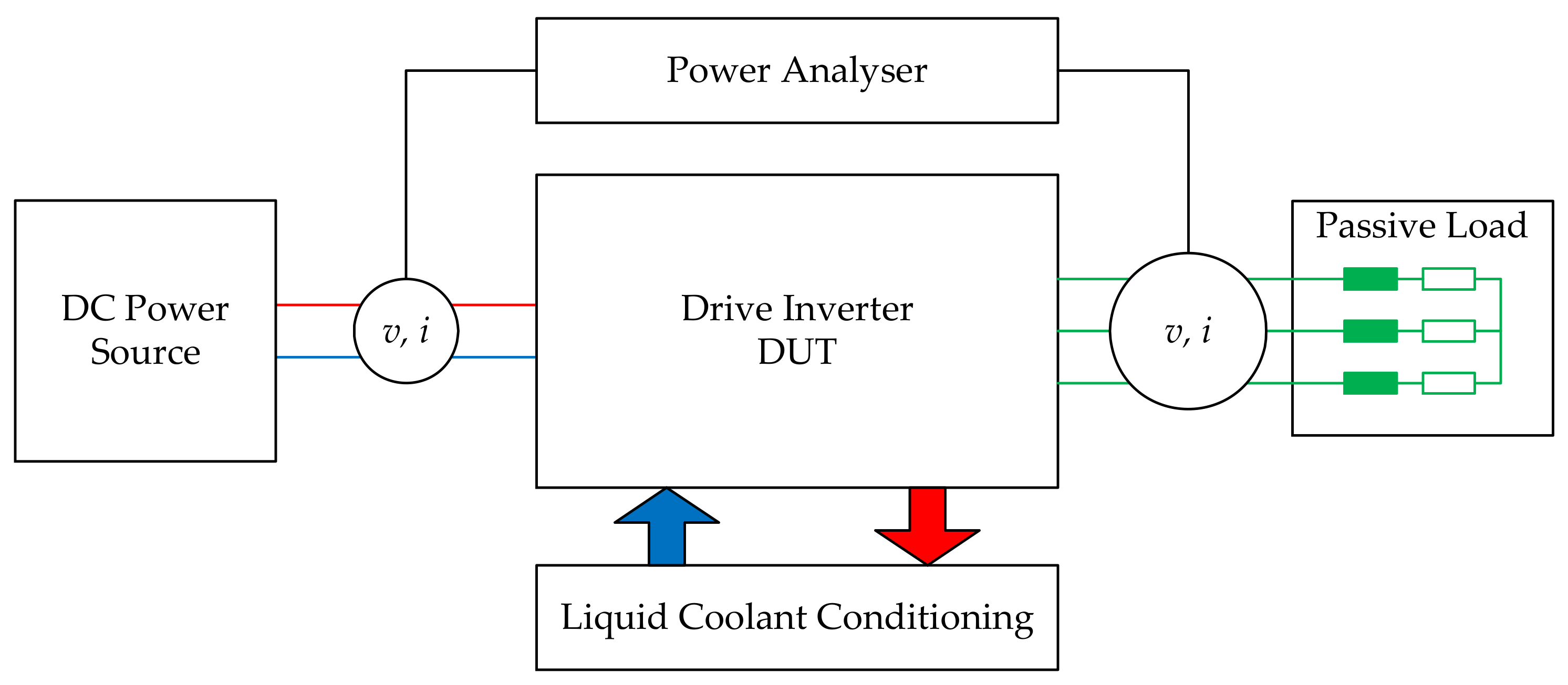
3.1. Measurement Setup for the Efficiency Analysis of Different Prototypes

In the test bench the inverters are supplied using a high-performance DC power supply. An adjustable passive load is formed using a three-phase inductor and a high power load resistor array. A cooling system with adjustable coolant temperature and flow rate is used to realise different environmental conditions according to the application’s requirements. The basic arrangement of these different components is shown in Figure 9.
Since the power stage prototypes do not include control electronics, the switching signals for the gate drivers and power devices are generated by an external microcontroller circuit. A conventional symmetrical space vector modulation with a fixed modulation index is used to create a symmetrical three-phase system with constant voltage and frequency in each individual steady state operating point. Thanks to a good linearity of the passive load, the resulting phase currents are also symmetrical and sinusoidal even without current control.
Thermal supervision of the inverter prototypes and their power devices is realised using applied thermocouple sensors and infrared thermographical observation. The switching speed and voltage overshoot behaviour of the power semiconductor devices is permanently monitored using a high bandwidth oscilloscope.
The most relevant electrical measurements serve the determination of power and losses. A high precision power analyser Yokogawa WT3000 and high bandwidth and high precision current sensors Danisens DS200 are used to measure both input and output electrical power. Especially for the AC output power measurement at a high switching frequency high quality equipment is needed and care must be taken in setting up the measurement parameters.

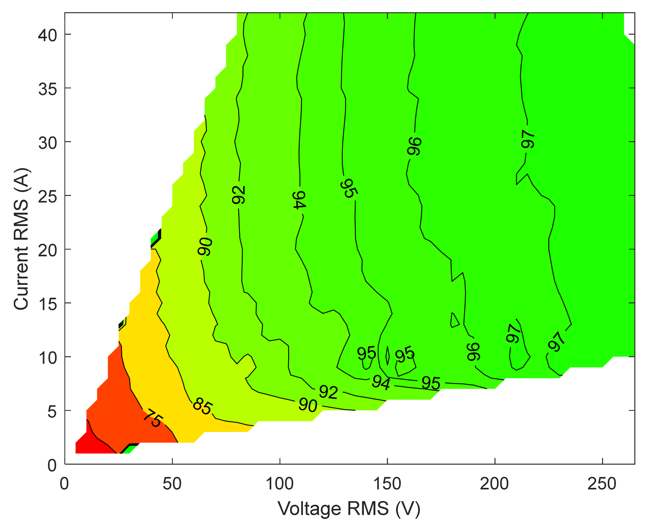
3.2. Measurement Results of the Reference Design

As a first device under test, a drive inverter that realises the reference design with three-level T-type half bridges using 650 V/1200 V silicon IGBT technology is operated in the test bench. For this inverter, measurement data for a complete efficiency map are collected. The results are shown in Figure 10. The inverter is operated at 400 V DC and a switching frequency of 30 kHz.
In the previously defined full load static operating point OP (2) at 42 A output current the measured efficiency is about 97.1%. Based on the modelling and loss estimation, an optimal efficiency of 97.7% was expected. The difference can be explained by additional losses in the DC link, the implemented filter elements, connectors and slightly increased switching losses of the power devices. Nevertheless, the measurement prooves a successful setup of the test bench components and good consistency of the loss estimation method and the practical evaluation.

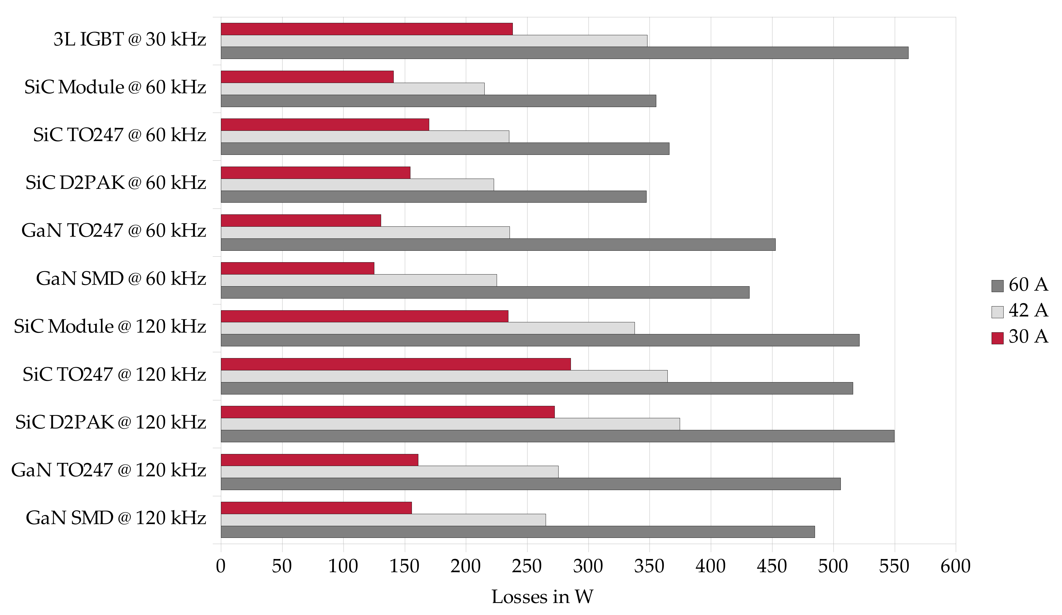
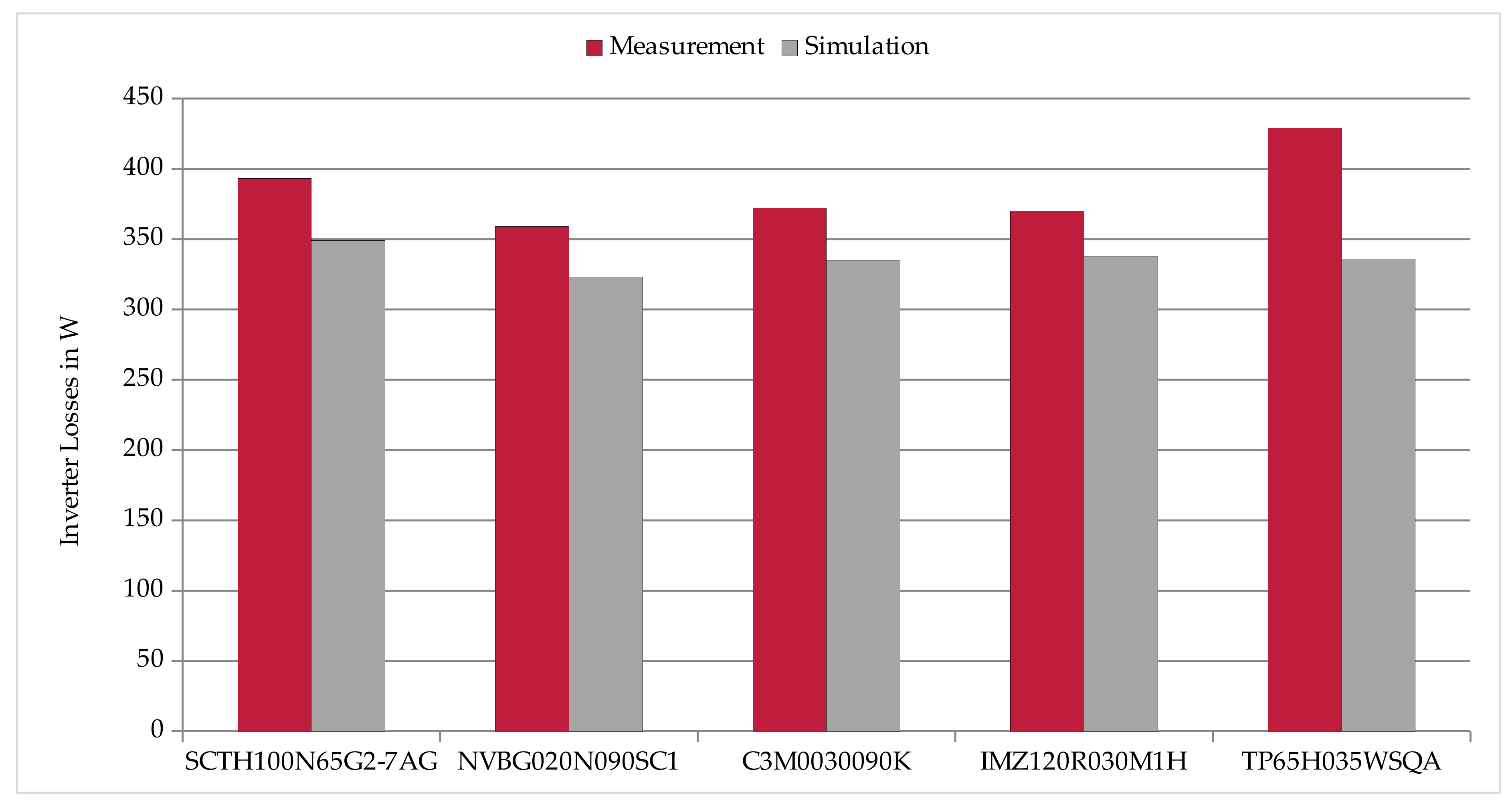
3.3. Measurement Results of the Wide Band Gap Power Stage Prototypes

In the next step the developed power stage prototypes using different wide band gap power devices in a simple two-level B6 inverter topology are operated in the test bench. At first, the switching behaviour, switching speed and voltage overshoot characteristics are investigated and tuned by adjusting the respective gate resistors. Unfortunately, not all prototypes can be operated successfully. Especially the selected GaN devices in cascode configuration show some difficulties in parallel operation as they tend towards massive ringing and insufficiently damped oscillations. Finally, the five configurations listed in Table 3 can realise stable operation and perform the efficiency measurements. Compared to the other devices, the 650 V silicon carbide MOSFET is tuned to a lower switching speed due to the small breakdown voltage safety margin.
During the efficiency measurements it can be recognised that the common mode capacitance of the passive load has a significant impact on the inverter losses at the investigated switching frequencies in the range from 60 kHz to 120 kHz. Therefore, it is measured separately using a RCL meter and taken into account in the loss estimation. Figure 11 shows the results of the measurements and the improved calculations, both for OP (2) at 60 kHz switching frequency for the five prototypes listed in Table 3.
It can be recognised that the losses are underestimated for all inverter prototypes. These additional losses may again be caused by the DC link, connectors and PCB resistances and capacitances that are not taken into account in the simulations. The difference between simulated and measured losses is in the range from 9% to 13% for the four different SiC devices.
For the GaN design, with 28%, the deviation between simulated and measured losses is significantly larger. To a certain extent, it is expected to be caused by an additional snubber circuit that is included in the design to improve the stability of the switching behaviour. Furthermore, additional losses seem to be caused by a still non-optimal switching behaviour and ringing of the parallelised devices. The leaded TO-247 package, that is not well suited for very fast switching devices, also contributes to these problems.
The key findings from the measurement-based investigation of the inverter efficiency are:
  • Silicon carbide MOSFETs can meet the requirements of this application and are easy to parallel.
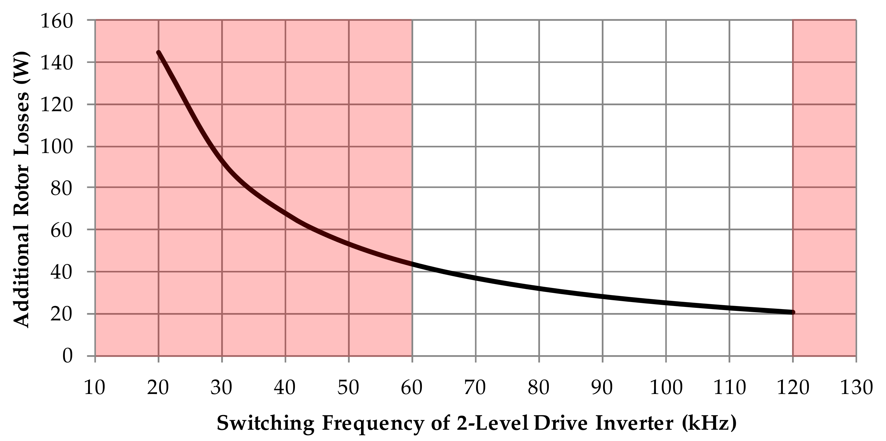
  • Switching frequencies of up to 120 kHz can be reached.
  • The loss prediction is fairly accurate.
  • The possible inverter efficiency is highly dependent on the load and its parasitic capacitance.
  • Surface mount devices have benefits in terms of size, parasitic inductance and ease of assembly, but good care must be taken designing an efficient cooling structure.
  • Certain GaN devices are difficult to operate in parallel, the TO-247 package is not well suited for these devices.

4. Reliability Analysis

New technologies for semiconductor materials, for example, wide band gap devices, offer many advantages in power density and weight. However, regarding lifetime performance considerations, they are relatively unknown. Semiconductors and their packaging technologies are tested with different tests. To find lifetime models concerning load cycles of a component, typically, power cycling tests must be performed. For resilient lifetime estimation, a large data basis consisting of many power cycling results is necessary. The number of published test results of discrete wide band gap devices is very low [22,23,24,25]. A power cycling test of one semiconductor can take several weeks or months depending on the test criteria.
The lifetime of power electronics and their components in the drive train of an electric vehicle or a hydrogen vehicle should achieve at least the same lifetime as a vehicle with a combustion engine, which might be 5000 to 8000 operating hours [26]. The battery of an electric vehicle has to last 160,000 km [27]. Depending on the vehicle’s medium speed of 30 km/h to 50 km/h, operating hour requirements between 3000 h and 5000 h can be derived. With 200 accelerations per hour the component has to last 6 × 10⁵ to 1 × 10⁶ cycles. Each cycle represents one temperature swing of the semiconductor chip.
In the following sections, lifetime calculations for discrete wide band gap power semiconductors are developed and presented. They are performed to check the different devices’ suitability for the specific application of a high speed drive inverter.

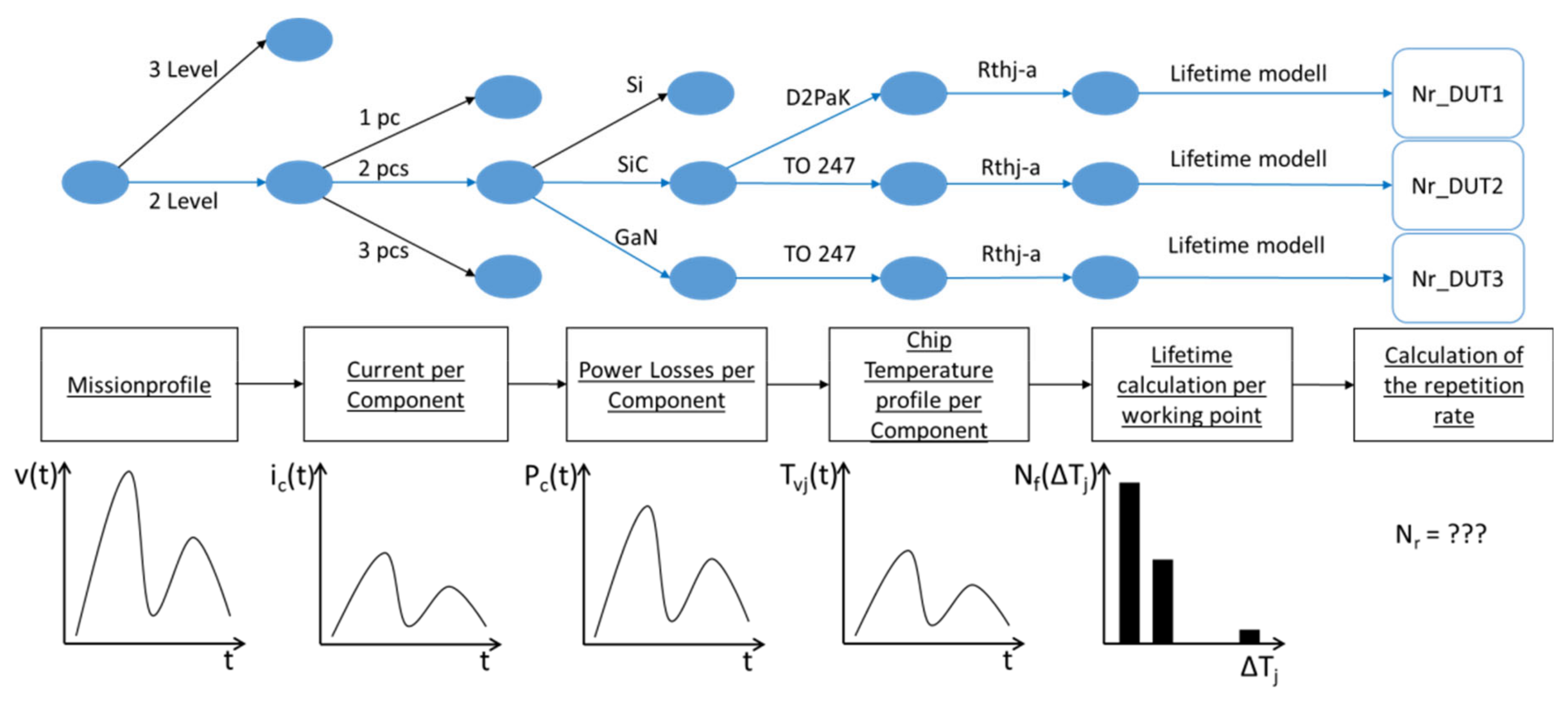
4.1. Lifetime Estimation Process

Often, the lifetime estimation is the last step in the design process of a device and it is based on many factors. Based on [28], a similar estimation process is used (see Figure 12). Depending on the requirements, the voltage class or the number of output voltage levels has to be chosen. Then, the number of components in parallel has to be set. After this, the available technologies, packages and cooling technologies can be chosen. Depending on the calculated operating hours, recursive loops have to be done. For example, the number of parallel components is set higher, or the cooling has to be changed until the desired results can be achieved.
Here, the lifetime estimation is done for a two-level inverter with two components in parallel (2 pcs) with ideal current distribution. This is the preferred configuration identified in the previous sections. Either silicon carbide (SiC) MOSFETs or gallium nitride (GaN) cascodes are used. The components have discrete packages like TO-247 and D²PAK with different thermal resistances between the case and cold plate (ambient).
Liquid cooling is very common in automotive applications. It efficiently limits the maximum junction temperature and guarantees a high power density. The calculations are done for most frequently used operating points (compare Table 2: OP (1) at 30 A and OP (3) at 60 A) and two different mission profiles.
The cycle number Nf of static operating points is calculated with the following equation that has been established for silicon devices over many years [29]:
N f = A   ·   Δ T j β 1   · exp ( β 2 / T j m i n + 273   K )   ·   t o n β 3   ·   I b β 4   ·   V C β 5   ·   D β 6
For the calculations, the common values for a standard IGBT power module listed in Table 4 are used, as no data for the discrete GaN or SiC components are available and the typical failure modes like bond wire cracks or lift offs are expected to be similar. Nevertheless, it is a rough estimation to get a first overview.
The limits are given by the parameters of the power cycling tests that have been done. The authors of [29] identified the parameters A and β1 to β6 by curve fitting of test results. For new technologies, they have to be adjusted.
Furthermore, it is assumed that all components are built up with three bond wires with a diameter of 300 µm, each. The bond wire current Ib should reach a maximum of 10 Arms, because the number of devices in parallel is two and the maximum load current of the inverter is 60 Arms. A bond wire lift off is expected to be the main failure mode, so the pulse time in power cycling tests is set to 1 s. For GaN cascodes, the inner structure is more complex since they are built using two different semiconductors.
Two different mission profiles are chosen for the dynamic stress calculations: One driving profile for the city (Figure 13) and one for the highway (Figure 14). Each profile has 3600 values and represents one operating hour.
The vehicle speed v(t) is converted into the current per component i(t). For every time step a loss calculation is done. Together with the individual thermal resistance of every component and the thermal resistance of the thermal foil and the cooling, the virtual junction temperature at every time step is calculated. The result is the temperature profile Tvj(t) of the chip temperature. This temperature profile is analysed with the rainflow algorithm which is explained in [30,31]. This gives a histogram with the numbers of different temperature swings. With the histogram and the following formula, the damage Qi of each component is calculated [32]:
Q i Δ T j , T j m i n , t o n , I b , V C , D = N i Δ T j , T j m i n , t o n , I b , V C , D N f i Δ T j , T j m i n ,   t o n , I b , V C , D  
Qi is the damage, Ni is the number of cycles from the mission profile, Nfi is the maximum number of cycles calculated for this operating point with Formula (1). The component is expected to fail when the damage Qi reaches the value 1.
To get the operating hours of the inverter, the reciprocal value of the damage Qi is used as shown in Formula (3). This is the repetition rate Nr of the mission profile [33]:
N r = 1 i = 1 n Q i = 1 N 1 N f 1 + + N n N f n  

4.2. Lifetime Estimation

The calculations are done for most frequently used operating points at 30 A and 60 A, a constant cos(ϕ) = 0.9 and two different mission profiles. Measurements of the thermal path of the used discrete components have shown that, for the thermal resistance from case to ambient (Rth,c-a), values of about 1.5 K/W and lower can be achieved. For the following calculations the value Rth,c-a = 1.5 K/W is used. A constant cooling temperature Tcoolant = 25 °C is assumed. A list of the different semiconductor components that were considered for the inverter is shown in Table 5.

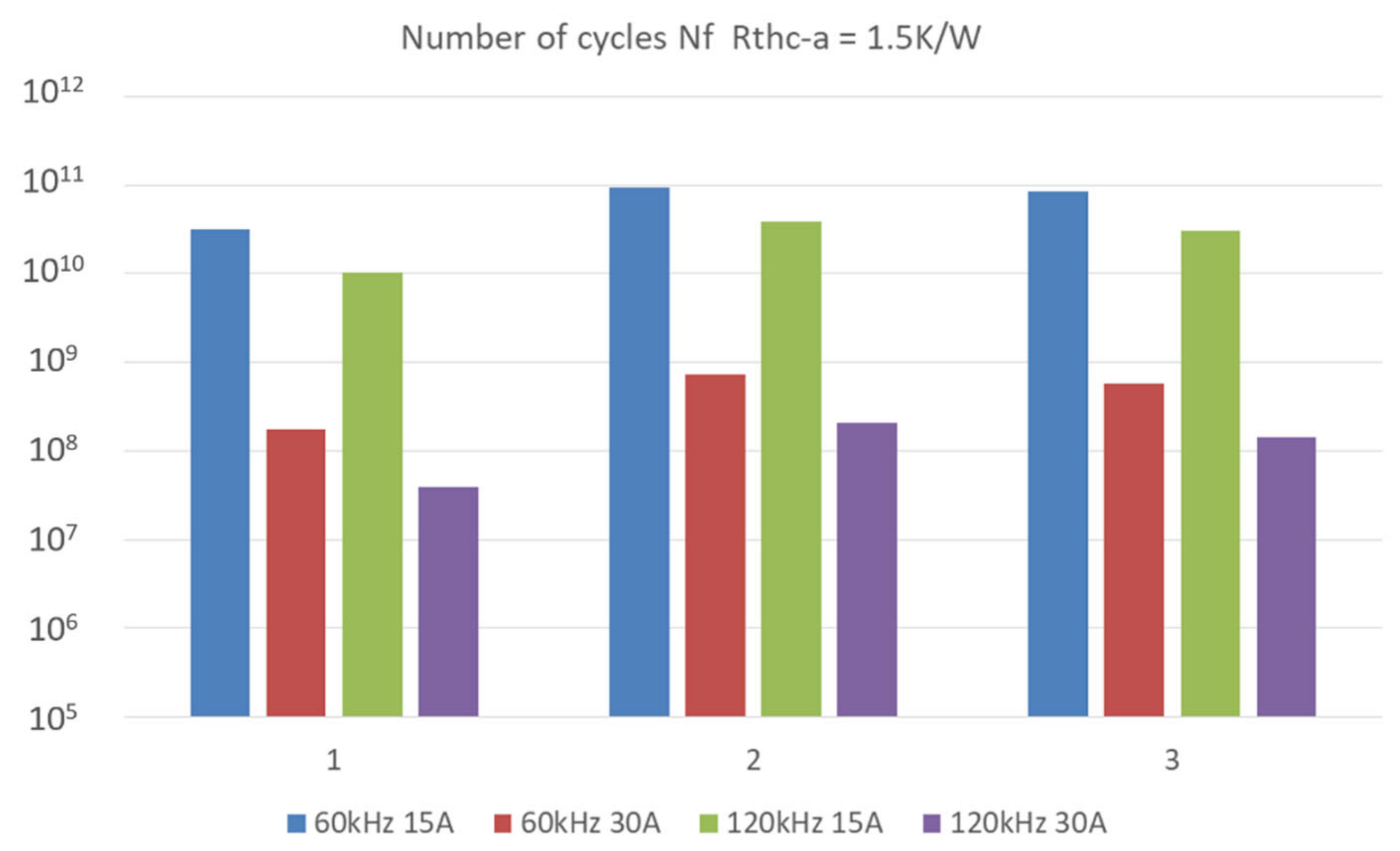
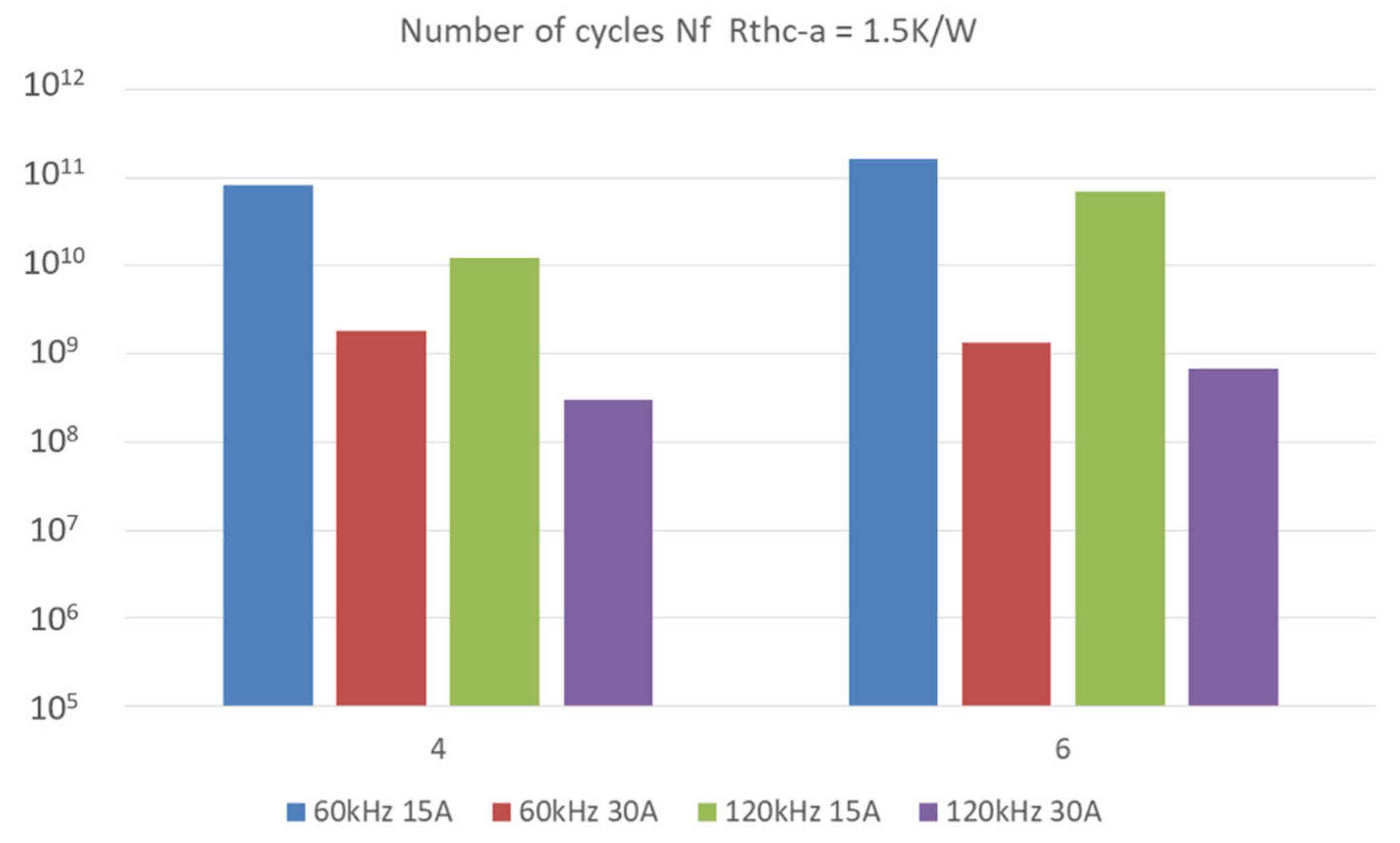
4.2.1. Estimated Lifetime for Static Operating Points

The switching frequency and the load current are varied, which influences the power losses. The power losses influence the temperature swings of the virtual junction. The thermal resistance from case to ambient influences the maximum value of the virtual junction temperature. Some results for the components listed in Table 5 (No. 1–12) are shown in Figure 15, Figure 16 and Figure 17.
Figure 15 shows the number of cycles of GaN components in the TO-247 package. The highest number of cycles is reached at 60 kHz and 15 A, which is the lightest load. The lowest number of cycles for each component is at 120 kHz and 30 A, which is the highest load. It can be seen that changing the load current from 15 A to 30 A has a bigger influence on the lifetime than changing the switching frequency from 60 kHz to 120 kHz.
The components are all in the same voltage class. The current rating, the on-state resistance Rds,on and the thermal impedance Rth,j-c of component 1 are different from components 2 and 3. This leads to higher temperature swings of component 1 and a lower number of cycles for every operating point.
Figure 16 shows the number of cycles of SiC components in D²PAK. The components have different voltage classes, different current ratings, different on-state resistance Rds,on and different thermal impedances Rth,j-c. The lifetime of these components is similar for 60 kHz. At 120 kHz the cycle number of component 6 is higher.
Figure 17 shows SiC components in TO-247 package. They belong to different voltage classes what means that the thickness of the dies is different. The current rating, the on-state resistance Rds,on and the thermal impedance Rth,j-c are also different, so the power losses and the cooling are different. However, all togethers the values of the temperature swings of the junction are about the same. The number of cycles is similar for these components.

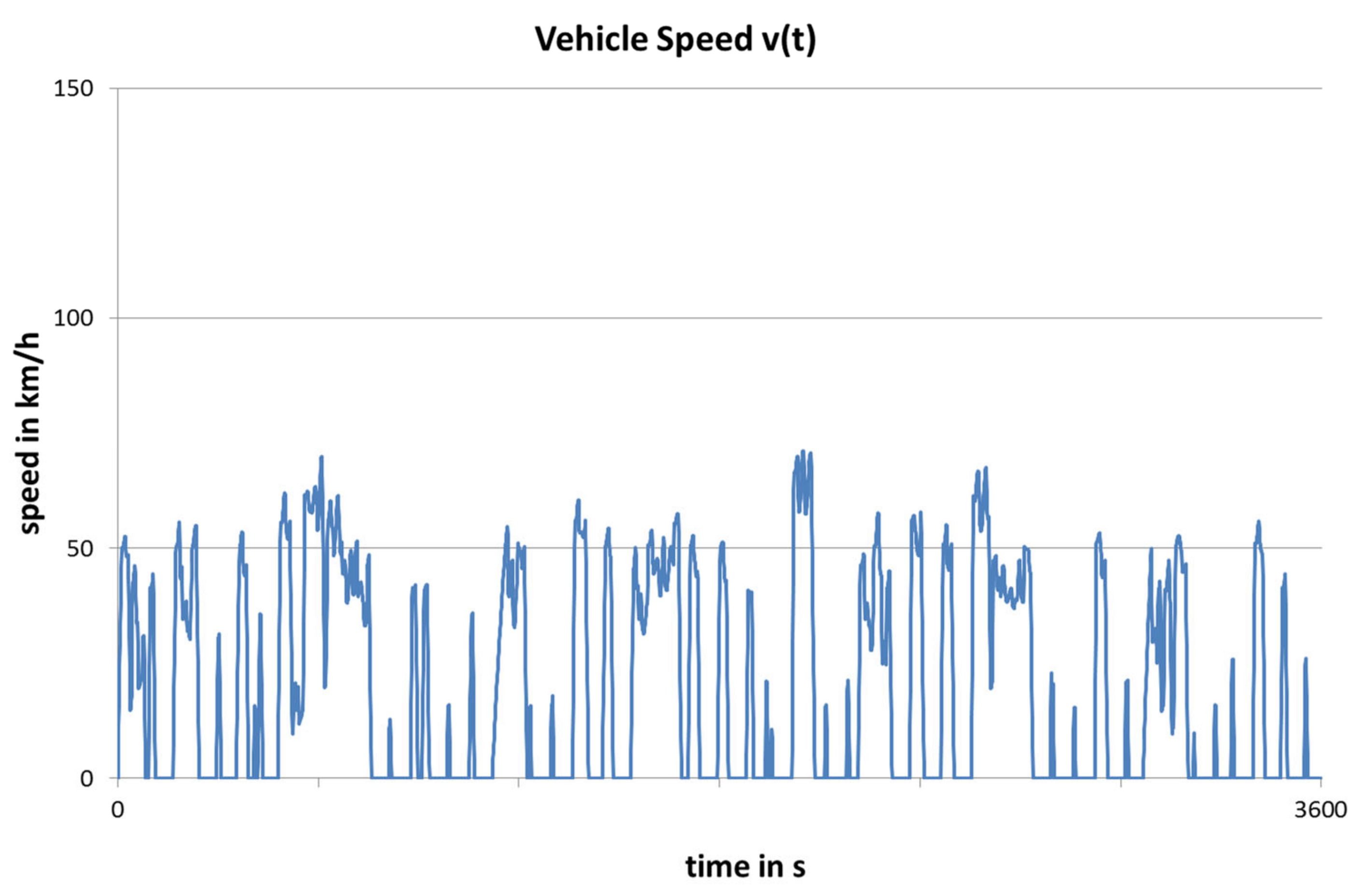
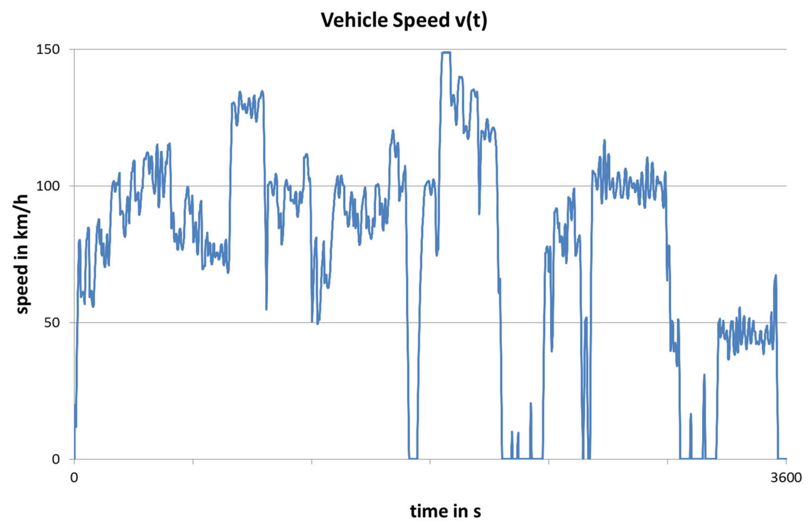
4.2.2. Estimated Lifetime for Mission Profiles

The lifetime estimation for variable stress of the components is done with two different mission profiles, a city mission profile (Figure 13) and a highway mission profile (Figure 14), which shall cover most of the use cases. The calculations are done with switching frequencies of 60 kHz and 120 kHz. The results for all components are shown in Figure 18 and Figure 19. The red lines indicate the required number of cycles for a medium speed of 30 km/h and 50 km/h and 3000 to 5000 operating hours.
The repetition rates Nr for the city profiles (Figure 18) are relatively high because the stress of the components is relatively low. Component 6 reaches the highest repetition rates, component 1 and 7 the lowest. Component 1 has higher power losses and component 7 has higher losses and a higher thermal resistance than the other components. The rainflow algorithm has detected 138 temperature swings for this city mission profile. All components are suitable for the inverter and this mission profile.
The repetition rates Nr for a highway profile (Figure 19) are lower than for the city profile. The stress for the components is higher because, at some time steps of the mission profile, the maximum load current is reached. Components 6 and 9 reach the highest repetition rates, component 1 and 7 the lowest. The rainflow algorithm detected 170 temperature swings for this highway mission profile. All components are suitable for the inverter and this mission profile.

4.3. Discussion of the Lifetime Estimation

A method for lifetime estimation for power electronics was presented. The lifetime estimation is based on a multitude of parameters. The parameters of the lifetime model have to be adjusted for SiC and GaN devices. That is why the presented results are a first estimation. The needed power cycling tests are still ongoing. The internal structure of the components make the lifetime estimation more complicated, because complex structures might have more complex failure modes. Tolerances of the inner structure of the components or in the thermal resistance are neglected but can also result in a higher junction temperature and a shorter lifetime. The number of bond wires and the bond wire diameter might be different for each component. A temperature profile for the ambient temperature could be added to get a more realistic temperature profile of the junction temperature. Dynamic stress with thermal capacities might lead to harsher stress and a shorter lifetime. The used mission profiles are exemplary and not representative like WLTP or NEFZ. In the future, lifetime aspects can be integrated in the dimensioning process.
The presented lifetime estimation shows that a lower switching frequency and the resulting lower switching losses are a better choice regarding lifetime performance. Nevertheless, the results for 120 kHz still show sufficient repetition rates for the use in the target application. A good cooling mechanism is essential to get the best performance as well as an acceptable lifetime.
The key findings from the reliability analysis are:
  • Since the connecting technologies of today’s wide band gap devices are similar to conventional silicon IGBT devices, the same failure mechanisms are expected and the same formulas can be utilised.
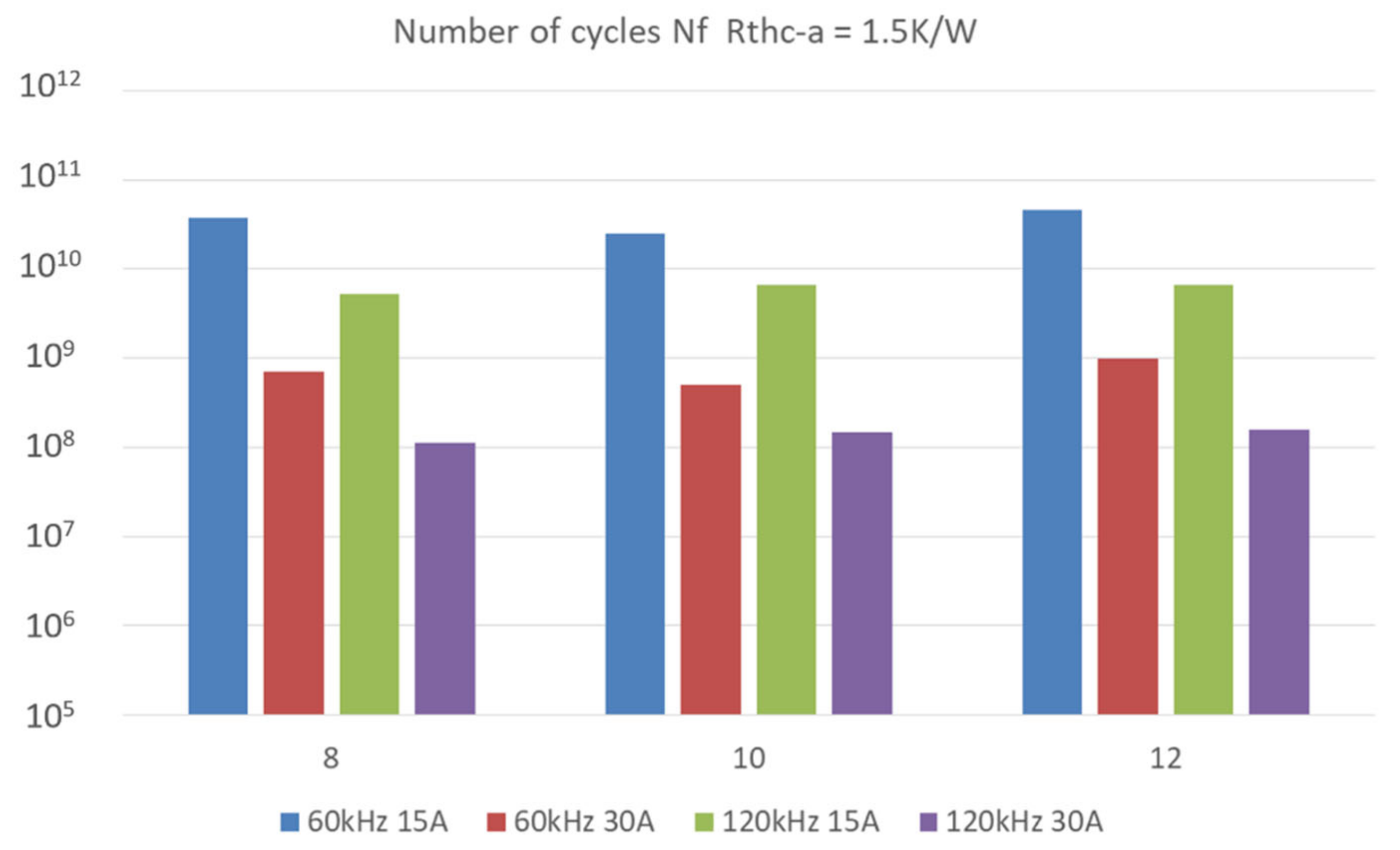
  • The number of possible cycles before a failure depends directly on the devices’ losses and temperature swings. Therefore, it decreases with a higher current and higher switching frequency.
  • Better cooling increases the number of possible cycles.
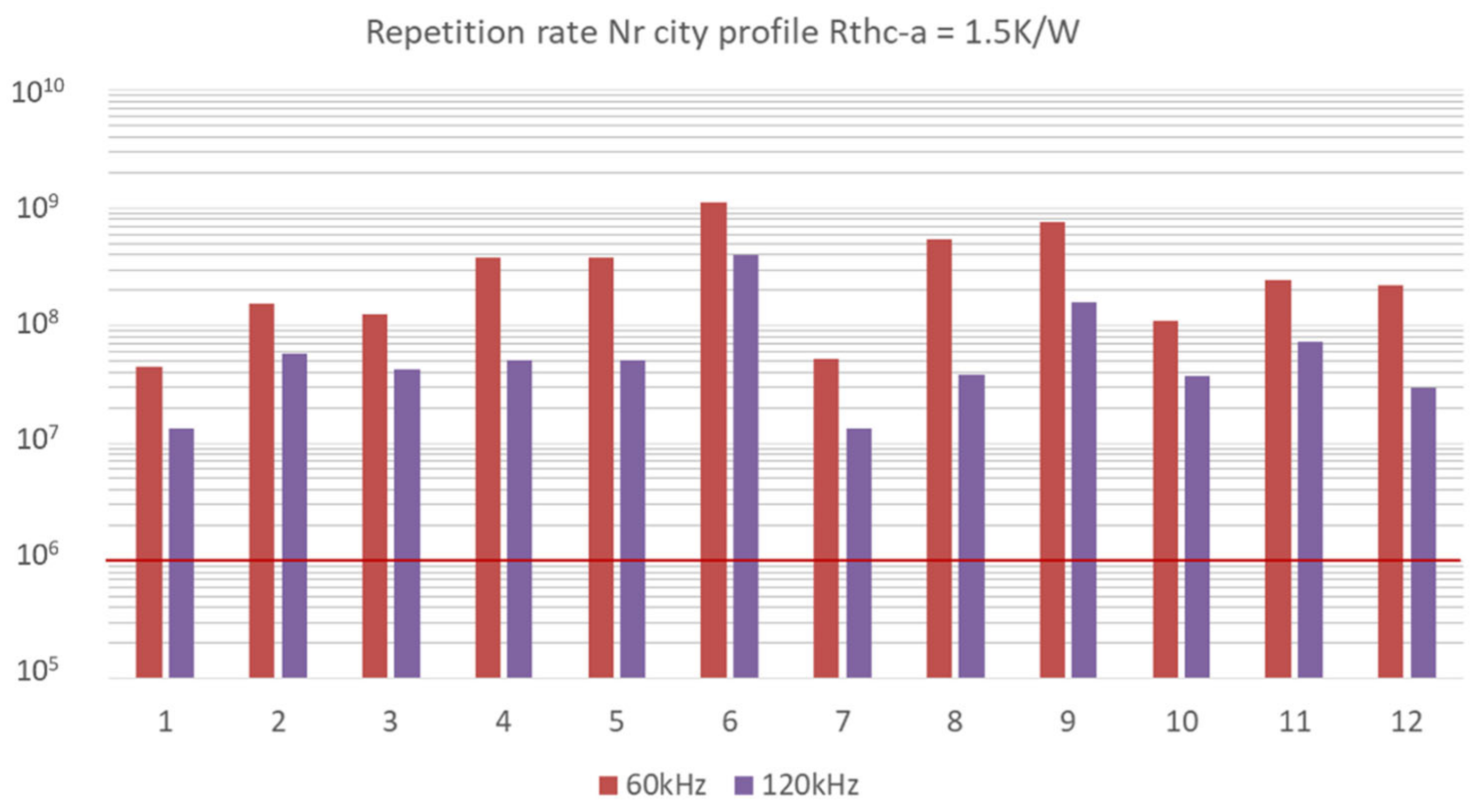
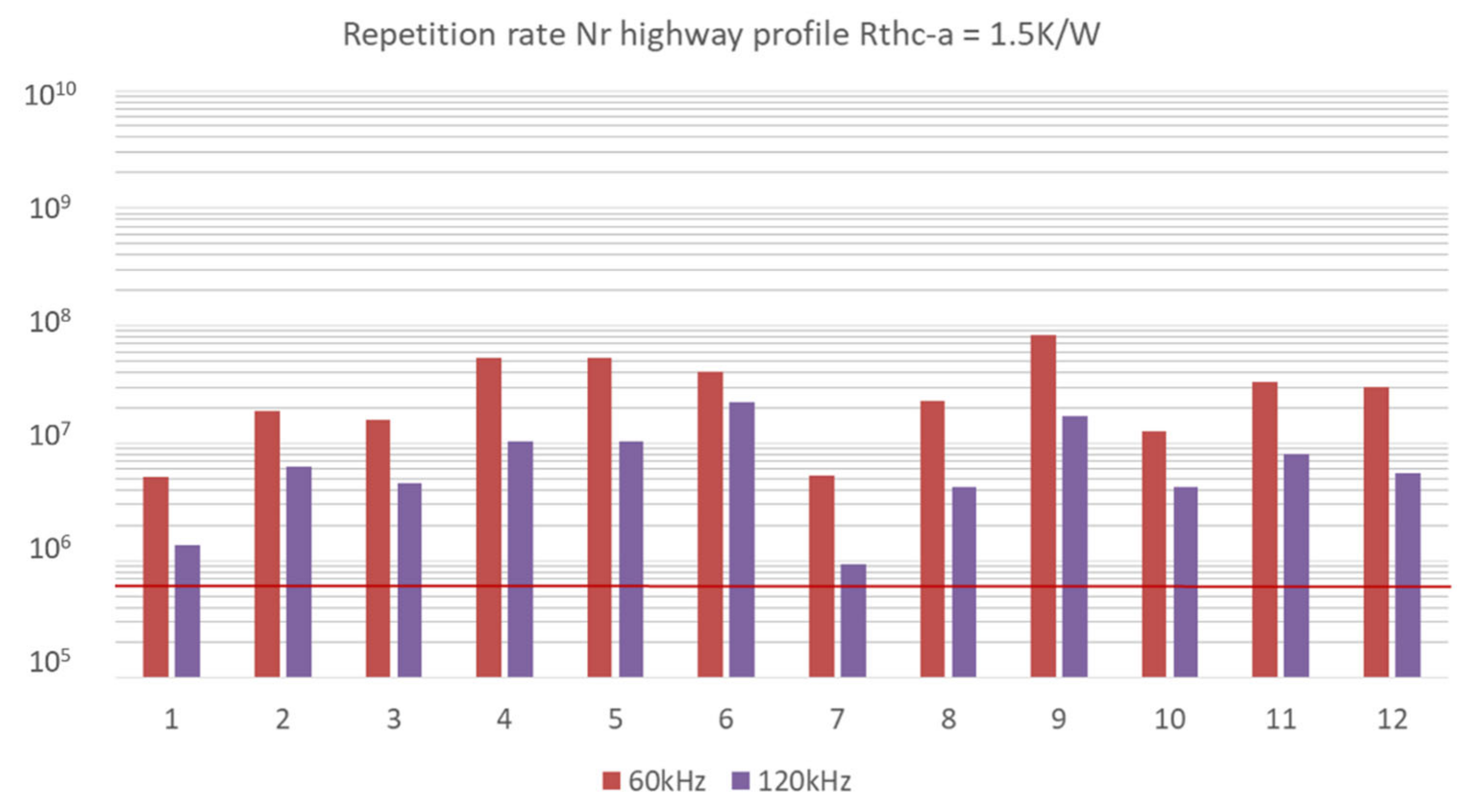
  • Using the rainflow algorithm, an expected repetition rate for different mission profiles can be calculated.
  • All devices are expected to meet the required reliability, even at a switching frequency of 120 kHz. Nevertheless, a design with low losses and good cooling should always be preferred.

5. Conclusions

In this article, recent research results on the design of a high performance, high speed drive inverter are presented. The given application of an electrical turbo compressor for automotive fuel cell systems gives challenging requirements like a high switching frequency as well as high efficiency and power density goals. Based on both simulations and measurements, it can be stated that solutions using wide band gap power semiconductor devices in a simple two-level inverter circuit can outperform a more complex three-level circuit of silicon IGBT devices in all of the defined evaluation criteria. The use of discrete surface mount power devices is the preferred solution for cost efficient mass production. It is shown that IMS PCB can help to reach low thermal resistances for these devices as well.
In addition to the device comparisons based on loss estimations, efficiency measurements and thermal investigations also comprehensive research on the lifetime and reliability of wide band gap power devices is performed and presented. It is shown that the selected devices are able to reach sufficient repetition rates and operating hours even at the highest expected switching frequency and under different mission profiles and load conditions. The parameterised lifetime models are currently validated by ongoing power cycling measurements.
All in all, the presented research covers many important aspects of future power electronics design processes. In particular, the consequent use of calculation methods, measurement equipment and lifetime models in the complete tool chain will be of increasing importance. With the maturing of SiC and GaN devices, design methods that can be used independently from a specific power device technology for all current and future devices that allows an easy and fair comparison of different devices for a specific application will be an urgent need.

Author Contributions

Conceptualization, N.L.; methodology, N.L. and F.L.; investigation, N.L., F.L. and D.H.; writing, N.L. and F.L.; visualization, D.H.; supervision, R.M.; project administration, R.M.; funding acquisition, R.M. All authors have read and agreed to the published version of the manuscript.

Funding

This research was funded by the German Federal Ministry of Transport and Digital Infrastructure, grant number 03B10105D. The APC was funded by the Open Access Publication Funds of Technische Universität Braunschweig.

Institutional Review Board Statement

Not applicable. No humans or animals involved.

Informed Consent Statement

Not applicable. No humans or animals involved.

Data Availability Statement

The data presented in this study are available on request from the corresponding author. The data are not publicly available due to pending non-disclosure agreements.

Acknowledgments

This work contributes to the project “Nationales Innovationsprogramm Wasserstoff- und Brennstoffzelle (NIP)-Phase II: Aufladung für Brennstoffzellensysteme durch interdisziplinär entwickelte elektrische Luftverdichter (ARIEL)”. The authors would like to thank all colleges working in the project and acknowledge the funding by the German government and the Open Access Publication Funds of Technische Universität Braunschweig.

Conflicts of Interest

The authors declare no conflict of interest.

References

  1. Balasubramanian, S.; Henke, M. Performance Evaluation of a High-Speed Permanent Magnet Synchronous Machine with Hairpin Winding Technology. In Proceedings of the 2020 International Conference on Electrical Machines (ICEM), Gothenburg, Sweden, 23–26 August 2020. [Google Scholar] [CrossRef]
  2. Boglietti, A.; Cavagnino, A.; Knight, A. Isolating the Impact of PWM Modulation on Motor Iron Losses. In Proceedings of the 2008 IEEE Industry Applications Society Annual Meeting, Edmonton, AB, Canada, 5–9 October 2008. [Google Scholar] [CrossRef]
  3. Boglietti, A.; Ferraris, P.; Lazzari, M.; Pastorelli, M. Change of the iron losses with the switching supply frequency in soft magnetic materials supplied by PWM inverter. IEEE Trans. Magn. 1995, 31, 4250–4252. [Google Scholar] [CrossRef]
  4. Yamazaki, K.; Abe, A. Loss investigation of interior permanent-magnet motors considering carrier harmonics and magnet eddy currents. IEEE Trans. Ind. Appl. 2009, 45, 659–665. [Google Scholar] [CrossRef]
  5. Van der Geest, M.; Polinder, H.; Ferreira, J.A. Influence of PWM switching frequency on the losses in PM machines. In Proceedings of the 2014 International Conference on Electrical Machines (ICEM), Berlin, Germany, 2–5 September 2014. [Google Scholar] [CrossRef]
  6. Schwager, L.; Tüysüz, A.; Zwyssig, C.; Kolar, J.W. Modeling and Comparison of Machine and Converter Losses for PWM and PAM in High-Speed Drives. IEEE Trans. Ind. Appl. 2013, 50, 995–1006. [Google Scholar] [CrossRef]
  7. Su, G.-J.; Adams, D. Multilevel DC link inverter for brushless permanent magnet motors with very low inductance. In Proceedings of the 2001 IEEE Industry Applications Conference. 36th IAS Annual Meeting (Cat. No.01CH37248), Chicago, IL, USA, 30 September–4 October 2001. [Google Scholar] [CrossRef]
  8. Shirabe, K.; Swamy, M.; Kang, J.-K.; Hisatsune, M.; Wu, Y.; Kebort, D.; Honea, J. Advantages of high frequency PWM in AC motor drive applications. In Proceedings of the 2012 IEEE Energy Conversion Congress and Exposition (ECCE), Raleigh, NC, USA, 15–20 September 2012; pp. 2977–2984. [Google Scholar] [CrossRef]
  9. Shirabe, K.; Swamy, M.; Kang, J.-K.; Hisatsune, M.; Wu, Y.; Kebort, D.; Honea, J. Efficiency Comparison Between Si-IGBT-Based Drive and GaN-Based Drive. IEEE Trans. Ind. Appl. 2014, 50, 566–572. [Google Scholar] [CrossRef]
  10. Lautner, J.; Piepenbreier, B. Performance Comparison of Cascode GaN HEMT and Si MOSFET based Inverter for Motor Drive Applications. In Proceedings of the IEEE PEDS 2017, Honolulu, HI, USA, 12–15 December 2017. [Google Scholar] [CrossRef]
  11. Morita, T.; Tamura, S.; Anda, Y.; Ishida, M.; Uemoto, Y.; Ueda, T.; Tanaka, T.; Ueda, D. 99. In 3% efficiency of three-phase inverter for motor drive using GaN-based gate injection transistors. In Proceedings of the 26th IEEE Applied Power Electronics Conference and Exposition (APEC 2011), Fort Worth, TX, USA, 6–11 March 2011. [Google Scholar] [CrossRef]
  12. Ding, X.; Zhou, Y.; Cheng, J. A review of gallium nitride power device and its applications in motor drive. CES Trans. Electr. Mach. Syst. 2019, 3, 54–64. [Google Scholar] [CrossRef]
  13. Morya, A.; Moosavi, M.; Gardner, M.C.; Toliyat, H.A. Applications of Wide Bandgap (WBG) devices in AC electric drives: A technology status review. In Proceedings of the 2017 IEEE International Electric Machines and Drives Conference (IEMDC), Miami, FL, USA, 21–24 May 2017. [Google Scholar] [CrossRef]
  14. Allouche, A. SiC MOSFET Comparison 2019; System Plus Consulting: Nantes, France, 2019. [Google Scholar]
  15. Ayari, T.; Gaalois, P. GaN Power Transistor Comparison 2020; System Plus Consulting: Nantes, France, 2020. [Google Scholar]
  16. Ding, H.; Li, Y.; Han, D.; Liu, M.; Sarlioglu, B. Design of a novel integrated motor-compressor machine with GaN-based inverters. In Proceedings of the 19th European Conference on Power Electronics and Applications (EPE’17 ECCE Europe), Warsaw, Poland, 11–14 September 2017. [Google Scholar] [CrossRef]
  17. Tüysüz, A.; Bosshard, R.; Kolar, J.W. Performance comparison of a GaN GIT and a Si IGBT for high-speed drive applications. In Proceedings of the 2014 International Power Electronics Conference (IPEC 2014/ECCE ASIA), Hiroshima, Japan, 18–21 May 2014. [Google Scholar] [CrossRef]
  18. Langmaack, N.; Tareilus, G.; Mallwitz, R. High Performance Drive Inverter for an Electric Turbo Compressor in Fuel Cell Applications. In Proceedings of the 22nd European Conference on Power Electronics and Applications (EPE’20 ECCE Europe), Lyon, France, 7–11 September 2020. [Google Scholar] [CrossRef]
  19. Langmaack, N.; Mallwitz, R.; Henke, M. Thermally optimised High Speed Drive Inverter Design using Surface Mount Silicon Carbide Devices. In Proceedings of the SIA Powertrain & Power Electronics International Conference and Exhibition, Paris, France, 9–10 June 2021. [Google Scholar]
  20. Langmaack, N.; Balasubramanian, S.; Mallwitz, R.; Henke, M. Comparative Analysis of High Speed Drive Inverter Designs using different Wide-Band-Gap Power Devices. In Proceedings of the 23rd European Conference on Power Electronics and Applications (EPE’21 ECCE Europe), Ghent, Belgium, 6–10 September 2021. [Google Scholar]
  21. Langmaack, N.; Schobre, T.; Henke, M. Fast and Universal Semiconductor Loss Calculation Method. In Proceedings of the 2019 IEEE 13th International Conference on Power Electronics and Drive Systems (PEDS 2019), Toulouse, France,, 9–12 July 2019. [Google Scholar] [CrossRef]
  22. Hoffmann, F.; Kaminski, N. Impact of Device Design on the Power Cycling Capability of Discrete SiC MOSFETs at Different Temperature Swings. In Proceedings of the ISPSD 2020, Vienna, Austria, 13–18 September 2020. [Google Scholar] [CrossRef]
  23. Xu, C.; Yang, F.; Ugur, E.; Pu, S.; Akin, B. University of Texas at Dallas Performance Degradation of GaN HEMTs Under Accelerated Power Cycling Tests. CPSS Trans. Power Electron. Appl. 2018, 3, 269–277. [Google Scholar] [CrossRef]
  24. Ziemann, T.; Grossner, U. Neuenschwander, J. In Power Cycling of Commercial SiC MOSFETs. In Proceedings of the IEEE 6th Workshop on Wide Bandgap Power Devices and Applications, Atlanta, GA, USA, 31 October–2 November 2018. [Google Scholar] [CrossRef]
  25. Franke, J.; Zeng, G.; Winkler, T.; Lutz, J. Power cycling reliability results of GaN HEMT devices. In Proceedings of the IEEE 30th International Symposium on Power Semiconductor Devices and ICs (ISPSD), Chicago, IL, USA, 13–17 May 2018. [Google Scholar] [CrossRef]
  26. Merker, G.P.; Teichmann, R. Funktionsweise von Verbrennungsmotoren. In Grundlagen Verbrennungsmotoren, 7th ed.; Springer Vieweg: Wiesbaden, Germany, 2014. [Google Scholar]
  27. ADAC Elektroauto-Batterie. Lebensdauer, Garantie, Reparatur. Available online: https://www.adac.de/rund-ums-fahrzeug/elektromobilitaet/info/elektroauto-batterie/ (accessed on 24 August 2021).
  28. Shen, Y.; Wang, H.; Yang, Y.; Reigosa, P.D.; Blaabjerg, F. Mission profile based sizing of IGBT chip area for PV inverter application. Proceedings of 2016 IEEE 7th International Symposium on Power Electronics for Distributed Generation Systems (PEDG), Vancouver, BC, Canada, 27–30 June 2016. [Google Scholar] [CrossRef]
  29. Bayerer, R.; Hermann, T.; Licht, T.; Lutz, J.; Feller, M. Model for Power Cycling lifetime of IGBT Modules - various factors influencing lifetime. In Proceedings of the 5th International Conference on Integrated Power Electronics Systems (CIPS 2008), Nuremberg, Germany, 11–13 March 2008. [Google Scholar]
  30. Mainka, K.; Schilling, O.; Thoben, M. Lifetime calculation for power modules, application and theory of models and counting methods. In Proceedings of the 2011 14th European Conference on Power Electronics and Applications, Birmingham, UK, 30 August–1 September 2011. [Google Scholar]
  31. GopiReddy, L.; Tolbert, L.M.; Ozpineci, B.; Pinto, J.O.P. Rainflow Algorithm-Based Lifetime Estimation of Power Semiconductors in Utility Applications. IEEE Trans. Ind. Appl. 2015, 51, 51–3368. [Google Scholar] [CrossRef]
  32. Ciappa, M. Lifetime Modeling and Prediction of Power Devices. In Proceedings of the 5th International Conference on Integrated Power Electronics Systems (CIPS 2008), Nuremberg, Germany, 11–13 March 2008. [Google Scholar]
  33. Lutz, J.; Schlangenotto, H.; Scheuermann, U.; De Doncker, R. Semiconductor Power Devices, 2nd ed.; Springer International Publishing: Cham, Switzerland, 2018. [Google Scholar]
Figure 1. Basic design process.
Machines 09 00350 g001
Figure 2. Additional rotor losses caused by high frequency stator currents.
Machines 09 00350 g002
Figure 3. Two-level voltage source inverter (2L VSI) using MOSFET devices.
Machines 09 00350 g003
Figure 4. Three-level neutral point clamped inverter in T-configuration (3L NPC T-type) using IGBT and diode devices.
Machines 09 00350 g004
Figure 5. Estimated inverter losses for selected two-level wide band gap inverter solutions [18].
Machines 09 00350 g005
Figure 6. Power stage prototypes using D²PAK (left) or TO-247 (right) device packages.
Machines 09 00350 g006
Figure 7. Half bridge power modules on IMS PCB, left to right: PQFN88, D²PAK, CCPAK1212.
Machines 09 00350 g007
Figure 8. Thermally optimised inverter prototype.
Machines 09 00350 g008
Figure 9. Inverter test bench scheme.
Machines 09 00350 g009
Figure 10. Measured efficiency map of the reference design (three-level NPC T-type, Si IGBT) [18].
Machines 09 00350 g010
Figure 11. Inverter power losses determined by measurement and simulation for OP (2) at 60 kHz.
Machines 09 00350 g011
Figure 12. Lifetime estimation method.
Machines 09 00350 g012
Figure 13. First mission profile of dynamic stress: City profile.
Machines 09 00350 g013
Figure 14. Second mission profile for dynamic stress: Highway profile.
Machines 09 00350 g014
Figure 15. Number of cycles of GaN components in TO-247 package with different operating points, Rth,c-a = 1.5 K/W, components 1, 2 and 3 with Rth,j-c = 1.05 K/W and Rth,j-c = 0.8 K/W.
Machines 09 00350 g015
Figure 16. Number of cycles of SiC components in D²PAK package with different operating points, Rth,c-a = 1.5 K/W, components 4 and 6 with Rth,j-c = 0.42 K/W and Rth,j-c = 1.1 K/W.
Machines 09 00350 g016
Figure 17. Number of cycles of SiC devices in TO-247 package with different operating points, Rth,c-a = 1.5 K/W, components 8, 10 and 12 with Rth,j-c = 0.84 K/W, Rth,j-c = 0.51 K/W and Rth,j-c = 0.27 K/W.
Machines 09 00350 g017
Figure 18. Repetition rate for a city mission profile, components 1 to 12.
Machines 09 00350 g018
Figure 19. Repetition rate for a highway mission profile, components 1 to 12.
Machines 09 00350 g019
Table 1. Basic functional requirements for the drive inverter [18].
PropertyValue
DC voltage 250 V to 500 V
Load currentup to 60 Arms
Load powerup to 15 kW
Load frequencyup to 2000 Hz
Switching frequencyat least 30 kHz (3-level) or 60 kHz (2-level)
InterfacesCAN, resolver, HV-interlock
Ambient temperature−25 °C to 90 °C
Coolant, temperaturewater/glycol, −25 °C to 70 °C
Table 2. Typical operating points defined for evaluation of different inverter designs [18].
PropertyOP (1)OP (2)OP (3)
DC voltage 400 V400 V400 V
Load current30 Arms42 Arms60 Arms
Modulation index0.90.90.5
Table 3. Successfully operated power stage prototype device configurations.
DevicesDescriptionGate Resistance (Ω)Voltage Gradient (V/ns)
(Always Two in
Parallel)
(Per Device)(For Two Devices)RisingFalling
SCTH100N65G2-7AGSiC 650 V, 20 mΩ, D²PAK2.215.8−14.4
NVBG020N090SC1SiC 900 V, 20 mΩ, D²PAK1.528.3−36.2
C3M0030090KSiC 900 V, 30 mΩ, TO-2472.732.4−36.2
IMZ120R030M1HSiC 1200 V, 30 mΩ, TO-2472.234.5−41.1
TP65H035WSQAGaN 650 V, 35 mΩ, TO-24715 (+3.9 per device)37.1−37.7
Table 4. Parameters and values used for the calculations with the CIPS08-Modell.
ParameterValueExplanationLimits
A2.03 × 1014Technology Factor
ΔTjvariable, depending on the loss calculationsTemperature swing of the chip45–150 K
Tjmin25 °CMinimal Temperature of the chip20–120 °C
ton1 sPulse time1–15 s
Ibvariable, divided by 3 1Current per bond3–23 A
Vcvariable, depending on the voltage classVoltage class of the chip600–3300 V
D300 µm 2Diameter of the bonds75–500 µm
β1−4.416
β21.258 × 10³
β3−0.463
β4−0.716
β5−0.761
β6−0.5
1 Assumption for the number of bond wires is 3. 2 Assumption for the diameter of bond wires.
Table 5. Component overview for the lifetime estimations with their most relevant parameters.
No.ComponentVoltageCurrentTechnologyPackageRth,j-c
1GAN063-650WSA650 V34.5 AGaNTO-2471.05 K/W
2TP65H035WSQA650 V47.2 AGaNTO-2470.8 K/W
3GAN041-650WSB650 V47.2 AGaNTO-2470.8 K/W
4SCTH100N65G2-7AG650 V95 ASiCD²PAK0.42 K/W
5SCTW100N65G2AG650 V100 ASiCTO-2470.42 K/W
6C3M0065090J900 V35 ASiCD²PAK1.1 K/W
7E3M0065090D900 V35 ASiCTO-2471.0 K/W
8C3M0030090K900 V63 ASiCTO-2470.84 K/W
9NTBG020N090SC1900 V112 ASiCD²PAK0.31 K/W
10IMZ120R030M1H1200 V56 ASiCTO-2470.51 K/W
11SCT3030KLHR1200 V72 ASiCTO-2470.34 K/W
12SCT3022KLHR1200 V95 ASiCTO-2470.27 K/W
Publisher’s Note: MDPI stays neutral with regard to jurisdictional claims in published maps and institutional affiliations.

