Review

Precision Machining by Dicing Blades: A Systematic Review

School of Mechanical Engineering, Shenyang University of Technology, Shenyang 110870, China
*
Author to whom correspondence should be addressed.
Machines 2023, 11(2), 259; https://doi.org/10.3390/machines11020259
Submission received: 14 January 2023 / Revised: 3 February 2023 / Accepted: 6 February 2023 / Published: 9 February 2023
(This article belongs to the Special Issue High Precision Abrasive Machining: Machines, Processes and Systems)

Abstract

:
Diamond dicing blades are profound cutting tools that find their applications in semiconductor back-end packaging and assembly processes. To fully appreciate the benefits of the dicing blade technique for precision machining, a deeper understanding is required. This paper systematically reviews the contribution of dicing blades in machining, followed by the context of dicing blades: production, characterization, methodology, and optimization. The readers are enlightened about the potential prospects that can be exploited for precision spectra as a result of current research and engineering developments.

1. Introduction

Dicing blades extend the capabilities of the traditional semiconductor process by allowing multiple microelectromechanical devices to be mounted on a single silicon wafer. Microelectromechanical systems (MEMSs) coupled with integrated circuitry (IC), infrared (IR) filter devices, and electromechanical components necessitate the profiling of hard and brittle materials such as silicon, silicon carbide and sintered silicon carbide (SiC and SSiC, respectively), alumina, quartz glass, sapphire, and dielectric substrates [1]. These materials’ wafer slicing results in miniature structures with complex patterns and structures. After being installed in devices, these microstructures must be reliable in harsh and corrosive environments. Such structures also need to have outstanding comprehensive properties such as high strength, increased hardness and stability, and improved wear capacity in postmachining scenarios. Back-end machining separates the chips from the wafer in order to fabricate the micro components. Microcracks and cracking that result in subsurface damage during machining can appear at the sidewalls and edges. Traditional subtractive machining techniques such as laser machining [2], electrochemical machining [3], and water/abrasive water jet machining [4] generate excessive chipping and cracking, which hinder the device from working effectively. In the context of failing to meet quality standards after the machining process, researchers sought a more precise machining approach. Dicing is a common machining technique that was previously used for micro texturing difficult-to-cut materials [5,6]. The traditional dicing method restricts the development of novel MEMS devices; however, over time, dicing blades and the dicing method have developed to produce high yield and throughput by allowing designers to create novel designs.
Among dicing, various techniques were used to carry out specific processes, such as die separation in the microelectronic industry, that used separation techniques such as diamond scribing (Figure 1a), laser scribing (Figure 1b), and diamond wheel dicing (Figure 1c) [7]. Ultrasonic dicing is another method of dicing that involves the simultaneous movement of abrasive grains impregnated in saw blades that carry rotational speed, an ultrasonic vibration perpendicular to the workpiece, and feed direction movement (Figure 1d) [8,9]. Apart from that, the stealth dicing technique focuses a laser beam on the surface beneath the target wafer (Figure 1e). Despite its ability to eliminate water damage concerns, its use is constrained because of issues with rough surfaces and heavily doped wafers [10,11]. Furthermore, plasma dicing allows for the cutting of a wafer into a die via dry etching under vacuum, which employs fluorine plasma to etch away the material in the dicing lanes between the chips (Figure 1f). It is appropriate for discrete devices with narrow streets and high aspect ratios to increase the fixing capacity of each die per wafer [12,13]. Each dicing technique has unique characteristics that present particular challenges.
ICs are mostly less affected by dicing challenges, whereas MEMSs are exposed to atmospheric variables during operation, making them more vulnerable to dicing challenges. A few factors must be taken into consideration in order to fully benefit from dicing blades for MEMS devices. The first challenge is contamination; large particles can stop moving devices, while small particles can disrupt device function. The MEMS structure limits the normal passage of particles that would generally be swept away with water sprayed on it as the wafer is being diced by the dicing blade. The second issue is water pressure damage and dicing forces. Because MEMSs can withstand less stress, water pressure and dicing forces must be kept to a minimum. The third is electrostatic discharge, which occurs when transferring a wafer between stations in a dicing saw and can affect electrostatic components. Some solutions have been proposed for contamination: modify the spray nozzle to change the flow of the nozzle; for water pressure damage, cap the wafer or protect it with a thin film. For forces, use an atomizing nozzle or immerse the wafer in water; for electrostatic discharge, use deionized water and ionizers [10,11]. Due to the characteristics of the material, the distribution of abrasive grains, the bonding matrix, and cutting parameters of feed speed, depth of cut, and cooling rate, dicing blades may exhibit defects such as delamination, fiber pull out, burrs, microcracks, chipping, nonlinearity, subsurface damage, and uneven cuts. A dicing method capable of meeting profiling needs is required to reduce dicing defects and improve surface characteristics.
Among various dicing techniques, the dicing blade is chosen for this review—a well-known technique subject to its widespread use for MEMSs and ICs by providing material grooving in addition to slicing, cutting off, cross-sectioning, and slotting [13]. While the use of dicing blades is important, it should not be the only metric to consider. Dicing blade production, dicing parameters (other than machining), and optimization are all viewed as proxies for dicing blade performance evaluation. In this review, to provide readers with comprehensive dicing mechanism guidance, we focused on the preparation, optimization, and applications of dicing blades, as well as the associated dicing technique, dicing blade characterization, and material removal mechanism.
Figure 2 depicts the search technique used for the review. The inclusion criteria are broadened to establish the database not only from Google scholar, Science direct, Web of science, etc. but also from technical reports from companies spanning the years 2000 to 2022. The paper is organized as follows:
I.
Section 2 explains the typical manufacturing process for different dicing blades, as well as the basic structure of a dicing blade. Meanwhile, critical steps for the success of each dicing blade are identified.
II.
Section 3 goes over specific actions to optimize the dicing mechanism. For example, preprocessing the dicing blade, developing a new blade, and modifying the dicing strategy can all assist stakeholders in achieving the best results.
III.
Section 4 describes dicing blade morphology, cutting force generation through cutting action, and machining-induced damages.
IV.
Section 5 focuses on the dicing parameters that influence the customized operation of the dicing process.
V.
Section 6 discusses the various material removal mechanisms that occur during the dicing of difficult-to-cut materials.
VI.
Section 7 sums up the role of the dicing blade in machining difficult-to-cut materials, forming waveguides, back-end IC processing, and micro texturing.
VII.
Section 8 ends the paper with key points and future prospects.

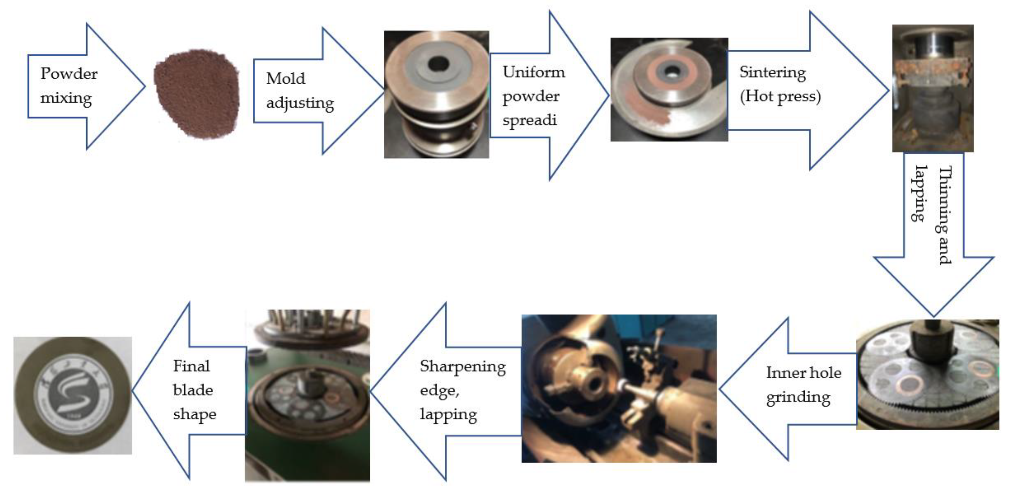
2. Preparation Methodology of Dicing Blades

The success of the complex dicing blade production process improves the dicing quality of the cut substrate, as shown in Figure 3 [15]. It begins with a ball milling machine mixing powder metals with diamond abrasives in proportion to the component ratio of the dicing blade. After measuring the volume and density of the mixed powder, it is filled in a graphite mold while another metal mold controls the thickness of the powder spread. Before transferring the mixed powder to the graphite mold for sintering in the hot press, the flat scraper removes the redundant powder from the mold. The thinning action on the sintered dicing blade is performed by a double-side lapping machine, and the uniformity of diamond grits is validated by a microscope. DISCO, ADT, Ceiba, Shanghai Sinyang, and UKAM are some of the leading manufacturers of dicing blades in China and across the globe [16].
Figure 4a depicts the structure of a typical dicing blade after production; the abrasive product of the blade contains three components: abrasives, bonds, and pores [13]. Abrasives are used to process the workpiece; they can be super or standard abrasives. Meanwhile, resin, metal, vitrified, and electroformed bonds hold abrasives to produce blades for quality cuts and air pockets hold abrasives in bonds (pores). Diamonds are recommended as abrasives for machining difficult-to-cut materials because they can precisely grind the material at the nano scale. Diamonds can be used as abrasives to cut through the hardest materials that cannot be cut through by conventional abrasives, carbides, or high-speed steel. High strength, wear resistance, and hardness make diamond an ideal candidate for machining hard-to-cut materials [17]. Synthetic diamonds are used for diamond blade manufacturing of resin bond, metal bond, and electroplating. Due to its consistency in shape, hardness, and density and usefulness for specific applications, the replacement of natural diamond with synthetic diamond is a lucrative option. High pressure high temperature (HPHT) and chemical vapor deposition (CVD) are two processes that can be used to create synthetic diamonds [18,19]. Belt, cubic, and BARS presses are the diamond-growing units in HPHT. Small diamond seeds, refined graphite, and catalysts made of metals and powders are all constituents of HPHT machines’ growth cells, which, when subjected to higher temperatures and pressures, transform into molten metal solutions. The carbon atoms in the dissolving graphite then create the diamond seed’s crystal structure over time. The diamond’s form is determined by the process parameters. Contrarily, in the CVD process, a mixture of gases, including carbon, hydrogen, and oxygen, fills the chamber. After heating the substrate, the diamond seed is added to the chamber, where carbon from the gaseous mixture eventually crystallizes into diamond.
The most common types of dicing blades are metal binder, resin binder [20], ceramic binder, hybrid, and electroplated nickel binder [16]; the first three can be produced using hot press sintering technology. In hot press sintering, sintering temperature and pressure ensure improved blade-cutting characteristics, and the heating process can be divided into transition, low-temperature alloy, and insulation stages. For pressure, it is gradually increased in three stages, beginning with the transition and ending with the final insulation stage [15]. Aside from hot press sintering [21], resin binder dicing blades can also be made using an ultraviolet curing technique, which turns liquid resin into solid resin [22]. The other widely used sintering methods are vacuum and spark plasma sintering (SPS) [23]; vacuum sintering prevents the flow of oxygen into the die while desorbing oxygen from powder metal. It should be mentioned that oxygen induction must be managed during the sintering process to avoid reactions brought on by the active element of carbon at higher temperatures. That could weaken the metal matrix’s strength and lessen the bonding force between the matrix and the diamond abrasive. Additionally, desorbing oxygen from the powder’s surface prohibits metal powders from oxidizing. In vacuum sintering, heating the wires with thermal radiation helps to heat the metal powder, so trying to adjust the temperature takes more time. The compound matrix is not uniform enough due to the longer time needed for the sintering process to complete [16]. Metal dicing blades made of SPS can achieve low sintering temperatures in a short period [24], ensuring that diamond abrasives are uniformly bonded to the matrix. The microstructures shown in Figure 4b are the result of an SPS process in which quick sparks occur between metal particles, resulting in metal particles that are very well merged in the matrix. In contrast, as shown in Figure 4c, a nonuniform matrix with reasonable porosity can be seen in the microstructure of the dicing blade emerging from vacuum sintering [16]. Electroplated nickel binder blades are produced by plating an ultrathin metal film on a substrate for diamond grit fixing [25].

3. Optimization of Dicing Blades

A few interventions can support the production of precise parts following dicing blade machining. The following subsections are enriched with descriptions of these interventions and their reciprocal effect on the quality of manufactured parts.

3.1. Through Truing

Truing a diamond dicing blade aids in determining spindle power consumption and mitigates chipping issues [26]. The use of trued and dressed blades for circumferential and sidewall grinding on high-hardness substrate materials such as Al2O3, Al2O3-TiC, and SSiC results in high energy consumption. High power consumption was observed for dicing SSiC due to increased sidewall wear in comparison to other materials Al2O3 and Al2O3-TiC. For dicing SiC in the presence of water, a thin polycrystalline diamond blade (PCD) trued by electrical discharge machining (Ed-trued) was used [27]. In contrast to excessive chipping with a nontrued blade, an Ed-trued blade produces sharp grooves and chip-free cutting edges, as shown in Figure 5.

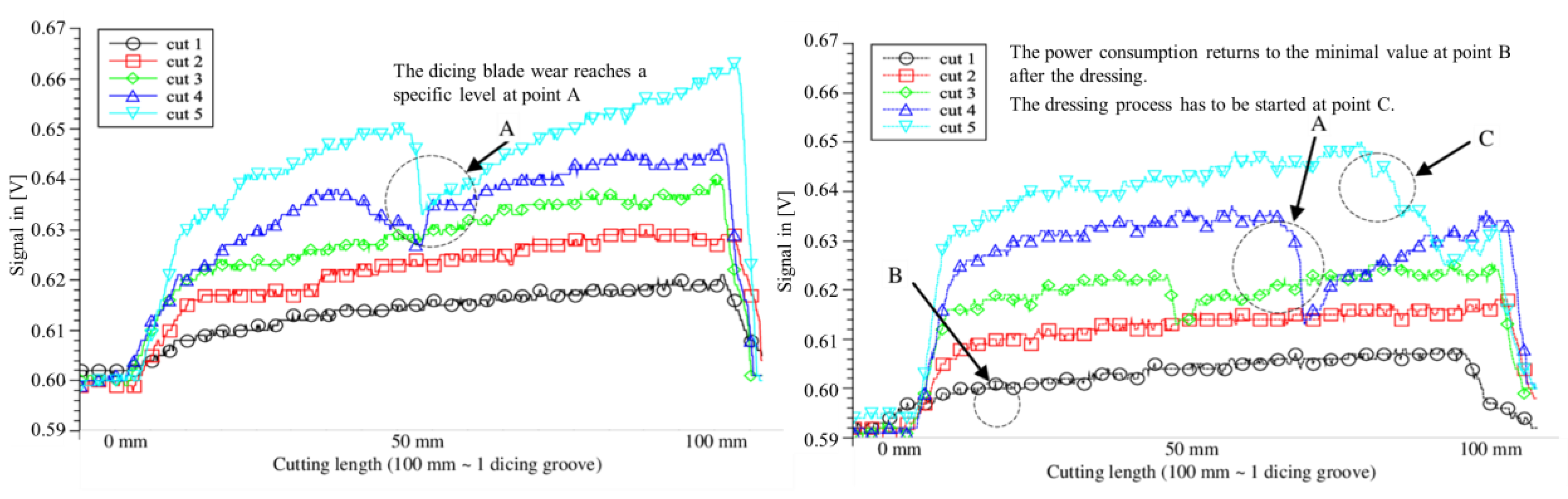
3.2. Through Blade Dressing

During the dicing blade preparation phase, dressing is defined as the process of removing excess bonding material by exposing sharp diamond abrasive grits for a better-quality cut. The use of dressing boards made of silicon carbide produced positive results in terms of capacity and production times, but the dressing process needs to be optimized to produce a dicing wheel topography that is positively correlated with blade profile, geometry, exposure, and cutting force [28,29]. Continuous laser dressing is possible in dicing machines by combining two capabilities: monitoring sharpness during dicing and performing laser dressing. As a result, researchers attempted to improve the performance of diamond dicing blades through laser dressing, keeping in mind that laser-dressed metal-bonded blades have high sharpness that aids in the processing of difficult-to-cut materials. Dressing on the cutting edge is accomplished by focusing the laser beam on the rotating dicing blade, and the chip space is created on the blade surface through the use of vaporization of the surrounding bonding material [29]. Dressing parameters can be adjusted to minimize the thermal influence on diamonds; dressing with a pulse duration of 12 ps provides the best dressing results by filling chip space with diamond abrasive grains to provide a maximum average roughness of Ra = 5 µm for wavelengths of 532 nm and 1064 nm, while less chip space produces a maximum average roughness of Ra = 3.41 µm for 655 ps pulse duration.
Moving from laser dressing to continuous laser dressing, where the dicing blade performs the cutting action and the abrasives wear out, laser irradiation helps to remove chips and metal binder from the blade so that the cutting process can be carried out with equal diamond protrusion, as shown in Figure 6. A pulsed laser with a pulse rate of τ = 655 ps and a wavelength of 532 nm can be used to install an on-machine laser dressing facility [30]. When compared to traditionally dressed blades, the laser-dressed blade achieved better cutting depth consistency. Investigations into the ability of nickel-bonded diamond blades to produce better results observed that the cutting depth and spindle power consumption stayed constant.
On-machine continuous laser dressing effectiveness can be assessed by monitoring spindle power and cutting depth consistency for hard and brittle materials such as aluminum oxide [1]. Since dicing wear is monitored by a power control attached to a spindle, laser-dressed blades demonstrated that blade sharpness is closely related to spindle power consumption, resulting in lower radial losses. Furthermore, dicing SSiC substrate with dressed blade produced better surface roughness, indicating that dicing blade grit size is also important as it leads to high sharpness for better kerf roughness and consistency in cutting depth [31]. In-line dressing criteria for metal-bonded diamond blades can be established; indirect analysis of cutting force measures the rotating spindle power consumption [32]. To elaborate criteria by dicing SSiC, after each cut, the cutting signal rises due to the amount of wear introduced in a specific instant of time, resulting in constant spindle speed. The dicing blade slips into the flange at point A and then sticks again, and as shown in Figure 7a, after crossing point A, the cutting quality changes. However, after dressing, the spindle’s power consumption reaches a minimum of 600 mV, as shown in point B of Figure 7b; the dressing process begins again at an 8 to 10% increase in spindle power, as shown in point C of Figure 7b; the blade then slips in the flange and sticks again (cut 3 and 4, Figure 7b). In-line detection of cutting defects can be performed, and after an 8 to 10% increase in signal, the dressing process must start to prevent further damage to the dicing blade.

3.3. Through Coating

To improve the performance of dicing blades, coating the cutting tools helps to reduce chipping levels and environmental aspects, such as less cooling water usage and less debris. Thin-film metallic glass (TFMG) coating on Si, SiC, and sapphire blades and patterned sapphire substrates (PSS) reduced chipping area by 23%, 36%, 45%, and 33%, respectively [33]. Similarly, titanium-aluminium-nitride (TiAIN) coating on nickel-bond diamond dicing blades improved hardness; the average hardness of the coated and uncoated blades measured was 0.41 Gpa and 0.1 GPa, respectively [34]. In addition to coating, BEO (1,4-bis(2-hydroxyethoxy)-2-butyne) can be added to the electrodeposition process of composite coatings during the preparation phase of dicing blades to improve hardness and wear resistance [35]. Although adding BEO to the bath helped to reduce chipping levels, coating on composite materials can help researchers find the best quality thresholds. To achieve composite coating on the dicing blades, a suspension and high–low speed interval agitation method was proposed [36]. According to the method’s findings, diamond concentration plays an important role in quality, so low grit sizes are recommended. Additionally, the diamond concentration was found to have a direct relationship with the suspended content and an inverse relationship with the stirring speed.

3.4. Through Adding Resin

Dicing blades commonly experience breakage; the strength can be increased by immersing the whisker in resin, which acts as a bonding material [37]. Apart from helping to strengthen the dicing blades, the light-sensitive resin has an instant solidifying process that uses less pollution and energy. The whisker in the resin greatly influences the mechanical properties of the light-sensitive resin. As a result, tensile strength increases with whisker quantity up to 15% by volume and then begins to decline. When a nonwhisker blade is compared to a whisker-added blade, the former ruptures after the dicing process, whereas the latter shows normal wear throughout. Furthermore, replacing thermosetting resin with photopolymerizable resin in the production of structure-controlled blades such as sandwich-structured, three-layer-structured, and slot-structured dicing blades improves machinability and lowers production costs [38]. Photopolymerizable resins with a slot-shaped mask that irradiates the resin with ultraviolet light can be used to create slot-structured blades. Three-layer blades improved in mechanical properties, while the grinding ratio and spindle motor improved as the number of slots increased. However, one disadvantage of using a slotted blade is that the chip size is larger because the workpiece, in this case, contacts more frequently due to the slots.

3.5. Through PCD Blade

PCD blades proved advantageous in the ductile-mode dicing process for resolving surface and chipping issues [39]. The fabrication of a PCD blade can be accomplished by tangentially irradiating the cutting edge of the rake and flank faces with pulsed laser light. Because of the PCD blade’s high stiffness and hardness, a surface with zero cracks and chipping emerged while undergoing full-cut conditions at high rotational speed; it also managed to cut a thick SiC substrate in one go while avoiding burr formation [40]. The developed PCD blade takes advantage of the feature of cutting in a straight line without buckling deformation in cemented carbide; ultrafine grooves with high aspect ratios of 50 were formed, i.e., 20 µm in width and 1 mm in depth, as shown in Figure 8. Due to the presence of distributed edges around abrasive particles, conventional blades are unable to produce such fine grooving; on the other hand, PCD blades have an agglomerated structure of uniform cutting edges for crack-free machining of the substrate.

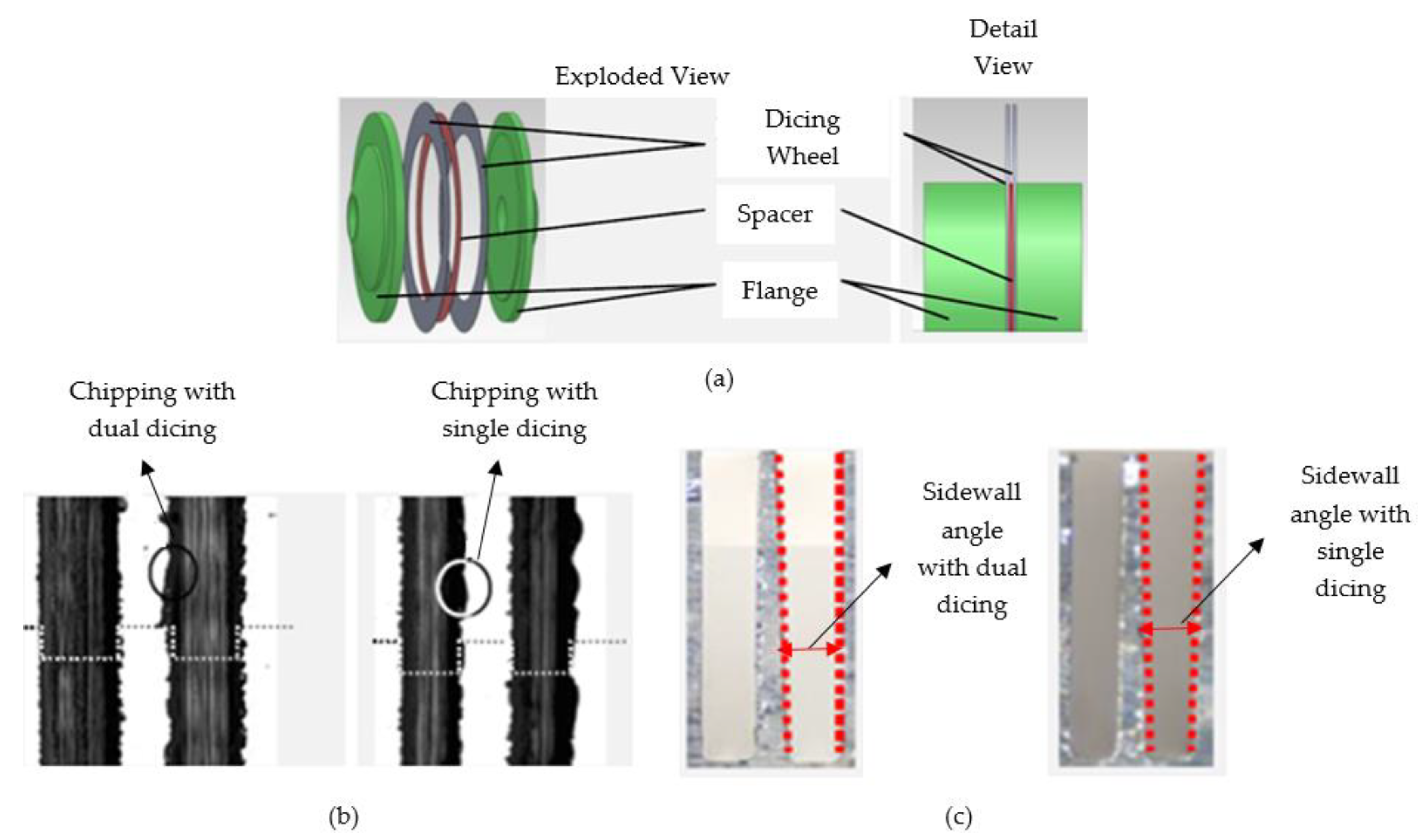
3.6. Through Dual Dicing

Figure 9a depicts the thickness of the spacer between two dicing blades and the diamond protrusion, which determines the size of the structure and helps to prevent excessive chipping and larger angles of the cutting groove sidewall [41]. Metal-bonded blades produced 20% less chipping than single dicing by using dual dicing on a stack of materials: anodically bonded silicon carbide, monocrystalline silicon, and borosilicate glass. Furthermore, when compared to a single blade, the outer sidewalls of the cutting groove with a dual blade gave smaller angles of less than one degree, as shown in Figure 9b,c. Although the dual dicing concept can produce microstructures with high aspect ratios, there are limitations regarding the chipping value, which must be less than 10% of the total thickness to prevent rupture. As a result, the impact of dicing blade protrusion requires better understanding. A double-pass sawing method, similar to dual dicing, was proposed to reduce chipping and cracking in silicon wafers laminated with conductive die attach film (DAF) [42]. Even though conductive laminated wafers frequently exhibit extreme chipping, the method found that dicing less than 30% of the DAF material resulted in less chipping.

3.7. Other Methods

The effective change in the bonding matrix during the dicing blade preparation phase allows for a robust dicing process [15]. To elaborate, three blades with different matrix compositions were developed to cut quartz and silicon, as shown in Table 1, and only the third dicing blade demonstrated good abrasive exposure, which aids in achieving a lower unit chipping coefficient. Contrary to dicing blade A’s alloy powders of CuSn33, CuZn20, and YA520 and dicing blade B’s alloy powders of CuSn40 and CuSn10, dicing blade C’s main matrix components are elemental metals. In comparison to elementary powders, alloy powders make dicing blades harder. As a result, while using dicing blades A and B, it is more challenging to expose diamond grits for matrix removal with dicing blade C. In contrast to dicing blades A and B, which have strong bonding strength, adding elementary particles during sintering reduces the bonding strength of dicing blade C, resulting in less edge chipping and, subsequently, a smaller chipping coefficient. Moreover, abrasive exposure and tool deviation coefficients were proposed to avoid edge collapse and chipping for cutting quartz and silicon.
Furthermore, the data-driven design of experiments (DOE) technique can be used to optimize the dicing saw parameters [43]. For example, by proposing a statistical analysis of variance (ANOVA) technique, an improvement in metal layer peeling and chipping was realized. While sorting out the significant parameters, the DOE model recommended high concentration and grit size blades, and specifically two factors, spindle revolution and cutting depth, were identified as significant factors for surface chipping with no impact on cutting speed. The DOE model can reduce experiment-related costs, but its accuracy can only be relied on if the blocking factors are fully accounted for. Electrophoretic deposition (EPD) was proposed to reduce chipping levels in hard-to-cut materials by using ultrafine abrasives to reduce the grain depth of the cut and thus minimize subsurface damage [44].

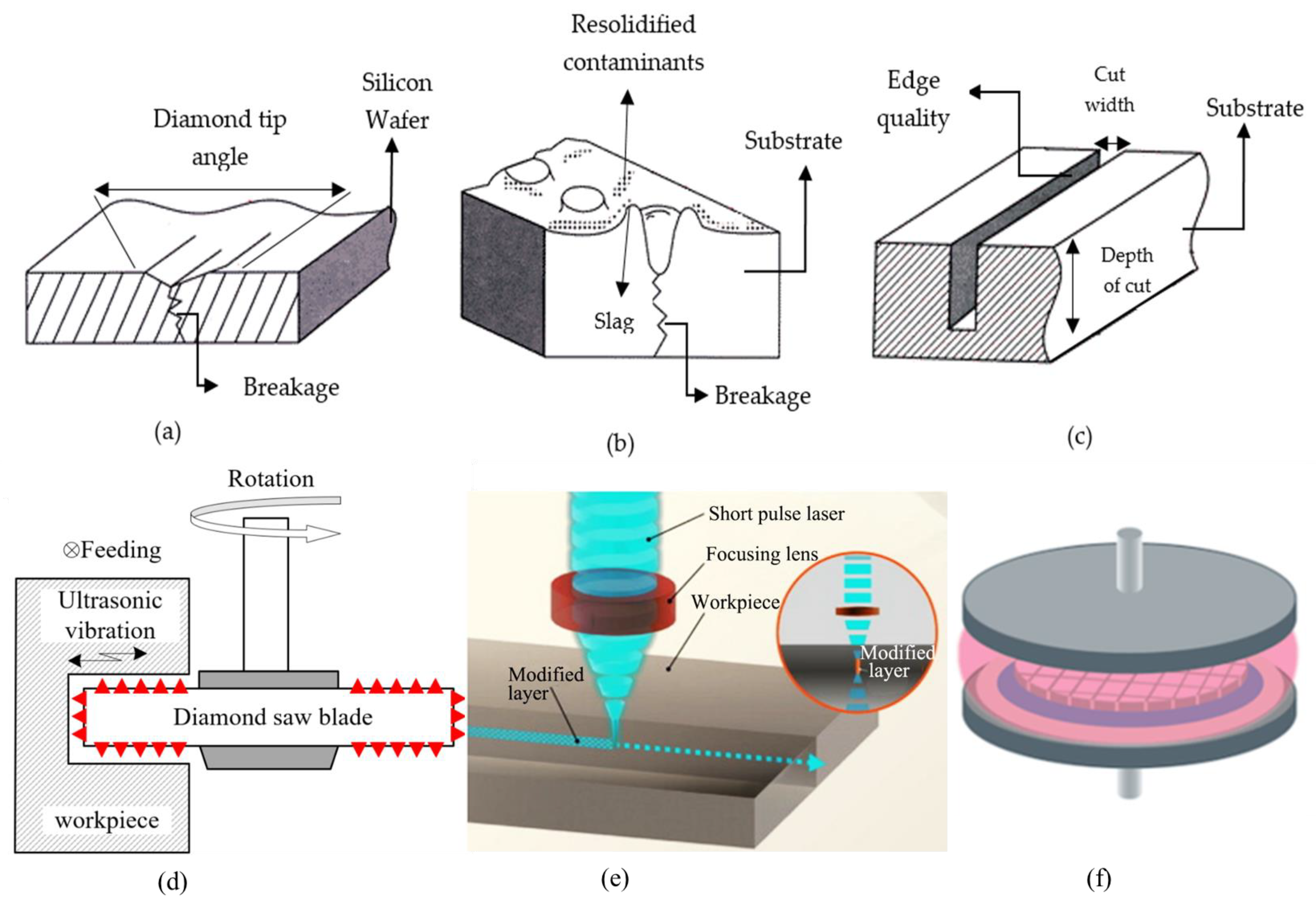
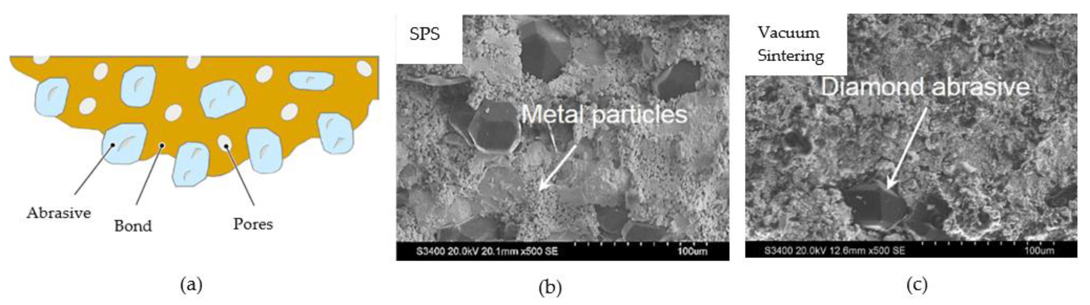
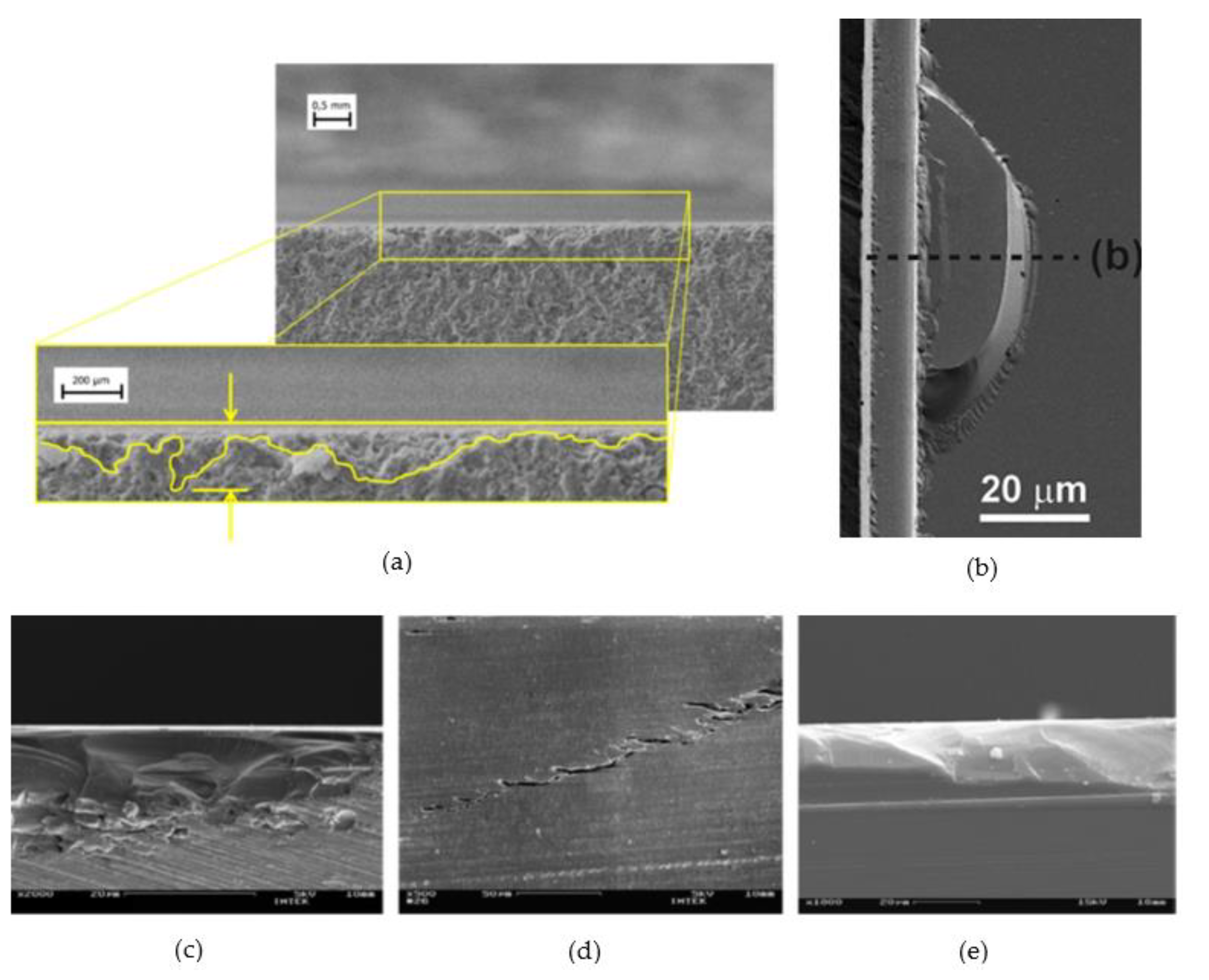
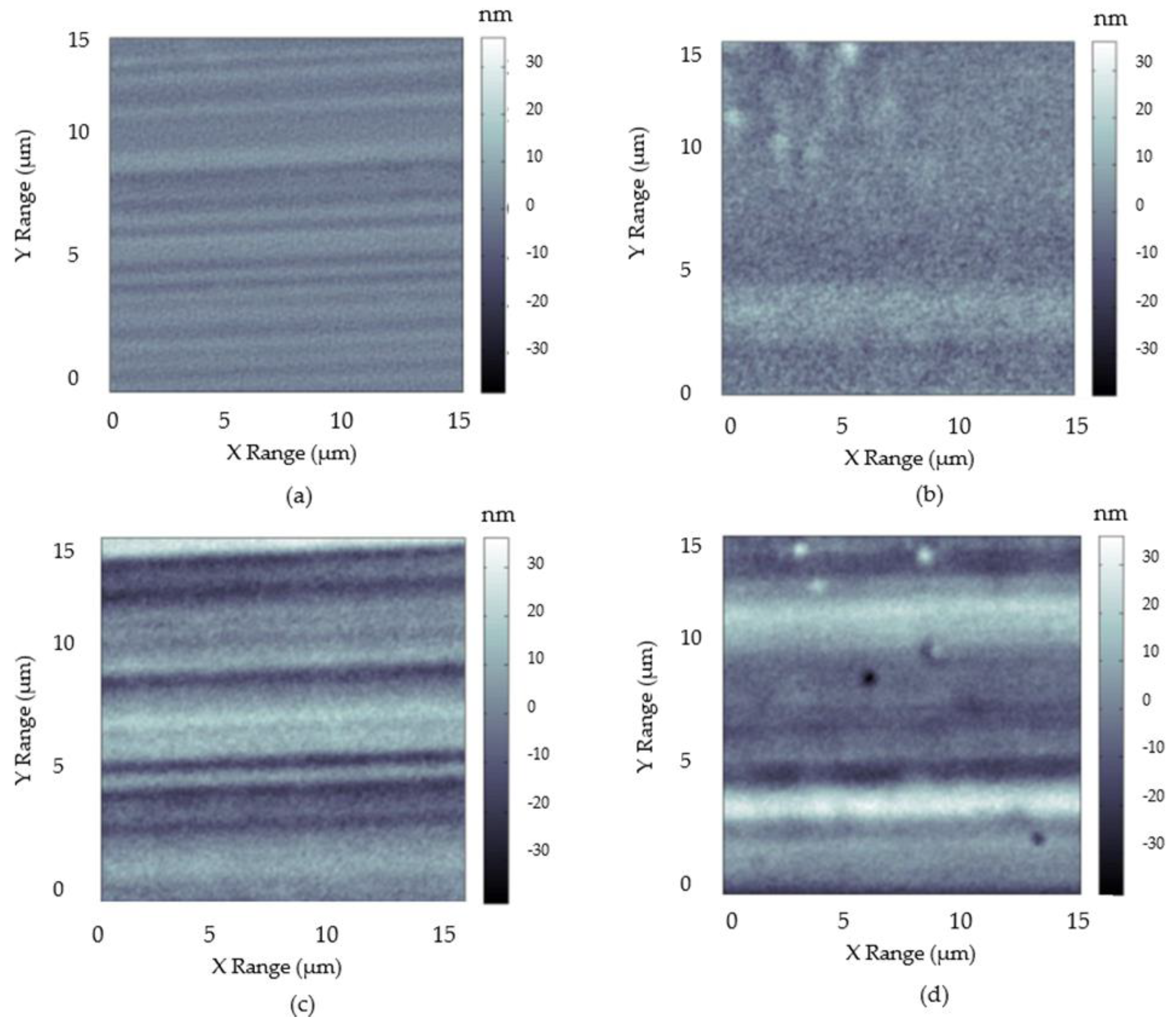
4. Characterization of Dicing Blades

Dicing machines produce precise parts for smooth operation with three cutting elements: a dicing saw, a laser saw, and a water jet saw [45]. Dicing saws are equipped with high-speed rotational bearings and abrasive blades that can achieve rotational and peripheral speeds of up to 60,000 rpm and 160 m/s, respectively, with a 51 mm blade diameter. While a laser saw uses a laser beam and CO2 or yttrium aluminum garnet (YAG) as a power source with different wavelengths, the process is capable of producing geometries other than straight ones in thin films [46]. Water jet saws use high-pressure water mixed with abrasive grains to cut at slower speeds. When compared to laser and dicing saws, the water jet saw is the least productive in terms of kerf quality but provides excellent thermal characteristics for curvilinear shapes [47]. Dicing saws are preferred over laser and water jet saws when material profiling requires micro thickness for cutting quality [45].
As mentioned in Section 2, a wide variety of dicing blades are available; the morphology of the target workpiece material and the profiling requirements guide the selection of an appropriate dicing blade. For example, the binder properties of metal-sintered diamond blades provide high rigidity and moderate matrix hardness, while thermal conductivity ensures a longer life span [16,48]. Resin-bonded diamond blades can provide a reasonable surface finish, high toughness, and less chipping whilst also having the downsides of shorter service life and less strength [49]. To mitigate the downsides, braze coating is recommended to improve diamond grit retention for resin-bonded dicing wheels that cover the facets of diamond grits with filler alloy [50]. Rapid wear reduces grinding efficiency and increases grinding force, which can be countered by SiC reinforcement, which improves wear resistance and ensures the wheel’s self-sharpening ability. Furthermore, due to the high diamond concentration, nickel-electroplated diamond blades provide quick cutting action with less heat generation [16]. A new type of Fe-based diamond saw blade with nickel-plated graphite particles is proposed; such blades with 2% graphite particles demonstrated good cutting capacity but were only assessed on rock samples [51]. Because each abrasive particle in a diamond dicing blade participates in the cutting action, the cumulative effect of all the embedded abrasive particles can be used to predict dicing forces. Elastic deformation, plastic deformation, chip deformation, and friction force between abrasive particles, binders, and substrate material all can be used to determine the level of dicing force. By ignoring tool wear, processing efficiency, dicing temperature, and vibrations, a theoretically determined dicing force produces remarkable results with high cutting speed and low feed rate and depth of cut [52]. Lower dicing forces generate less chipping [53]; this demonstrates the significance of dicing force as a factor in determining dicing quality.
The optical microscope and scanning electron microscope (SEM) can both identify dicing damage [45]. Using the pixel method, a unit chipping coefficient was proposed to quantify the chipping levels. The method quantifies chipping, and the final chipping measurement is the average of dimensions obtained in the predefined cutting length shown in Figure 10a. Damage can be reduced by controlling the vibration of the blades caused by spindle rotation and the cutting depth [54]. Simulation results also revealed the increase in the vibration with the increase in tool diameter and speed [55]. The delamination interface on a directly bonded wafer can be identified by taking a cross-sectional image of the chipping area from SEM; the center of a 20 m chipping is shown in Figure 10b [56]. During the separation process, damages due to dicing were observed by SEM and categorized for mechanical, thermal, and chemical loads [57]. Chipping at the front and back side edges is a mechanical load characteristic shown in Figure 10c–e, and the size of damage could be greater than 50 µm based on the dicing technique utilized.

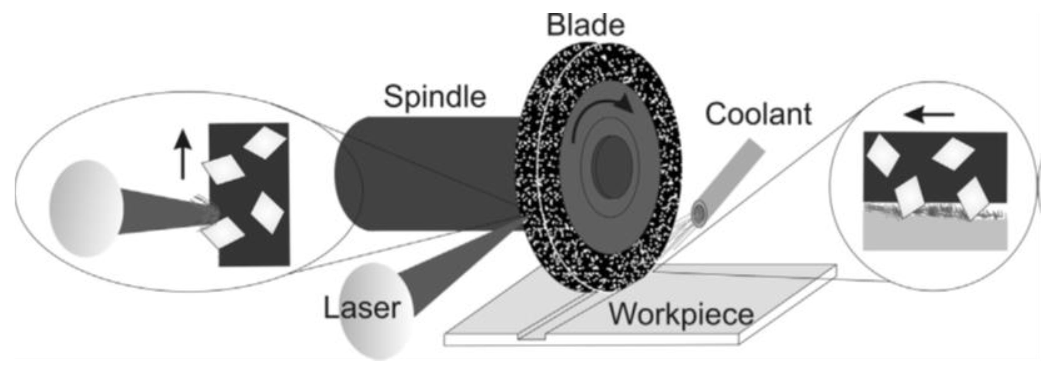
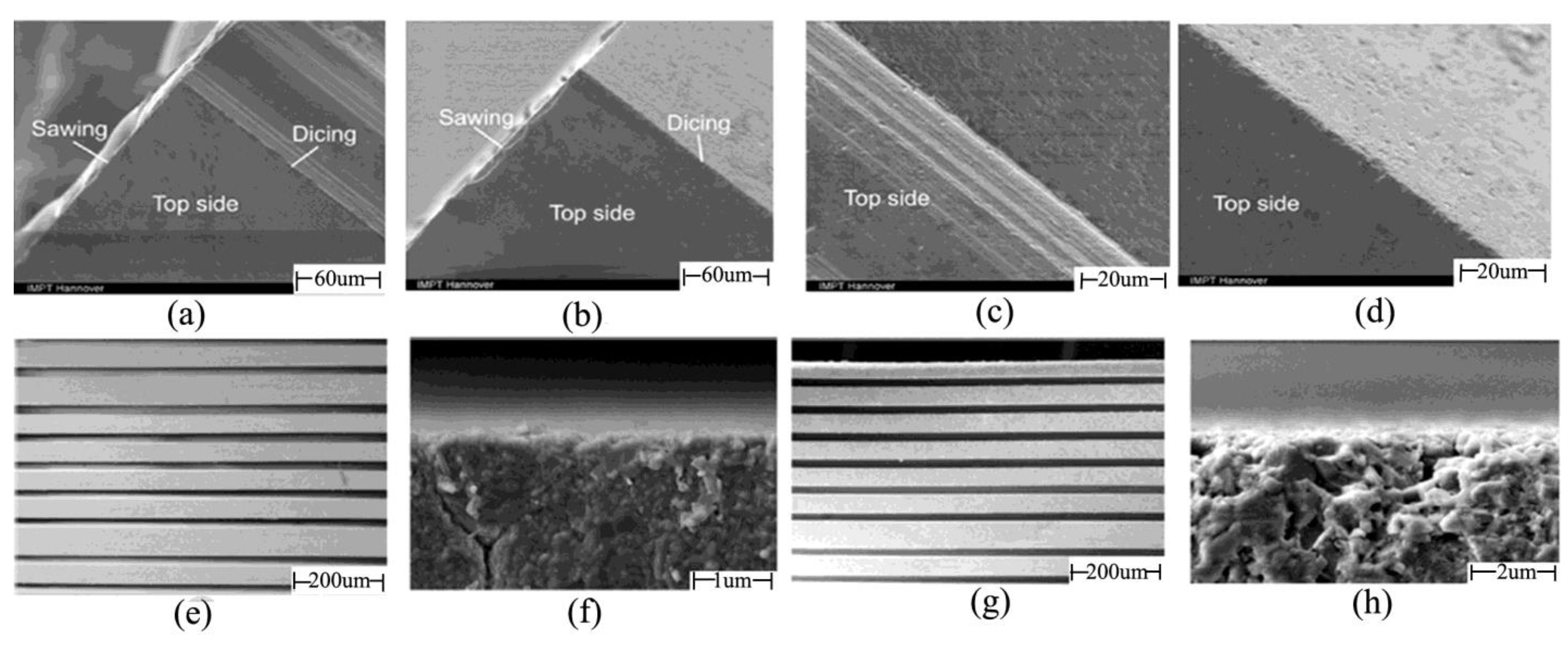
5. Dicing Technique of Dicing Blade

Unlike other cut-off machines, dicing blades used in dicing machines provide precision and repeatability; the dicing technique is assessed by evaluating edge quality, chipping levels, cracks, and surface roughness values [45]. Maintaining precision with complex influencing parameters such as diamond abrasive proportion and size, matrix structure, bonding strength, and porosity of dicing blades is difficult. The size and proportion of diamond concentration during the powder mixing phase must be adjusted taking into account the material to be cut, bond type, bond hardness, and cutting speeds. Figure 11 shows the dispersion of diamond abrasive particles in the dicing blade; a high diamond concentration leaves no room for debris to escape, whereas a low diamond concentration allows debris removal while maintaining the quality and surface finish of the cut substrate [52].
Bonding strength and porosity, which are entirely dependent on the sintering method, are key factors in the dicing process. The bonding strength between diamond grits and matrix determines the maximum cutting force of diamond grits that can act on the target matrix material bearing the fall of diamond grits from dicing blades, which defines the range of cutting damage. To deal with the stresses induced above the breaking strength that causes chip fracture, a model was formed incorporating both stresses and chip breaking strength to avoid such fractures [57]. But apart from that, coating strengthens the bonding of the dicing blades. Coating materials such as cobalt, nickel, iron, titanium, tungsten, and others are preferred because they can easily react with a diamond at high sintering temperatures. Furthermore, for alloys with low melting points and defected porosity, strengthening elements such as silicon carbide, cubic boron nitride (CBN), and alumina particles are mixed with powders for proper functioning with diamond grits. Matrix hardness in dicing blades is related to the exposure content of diamond grits; commonly used matrix mixes are copper-tin, copper-tin-cobalt, copper-tin-zinc, and copper-tin-titanium alloys. Furthermore, eight aspects (sharpening, strengthening, supporting, combination, wear resistance, reduction, toughening, and moistening) were identified to evaluate the effect of the interaction mechanism for the dicing factors [15].

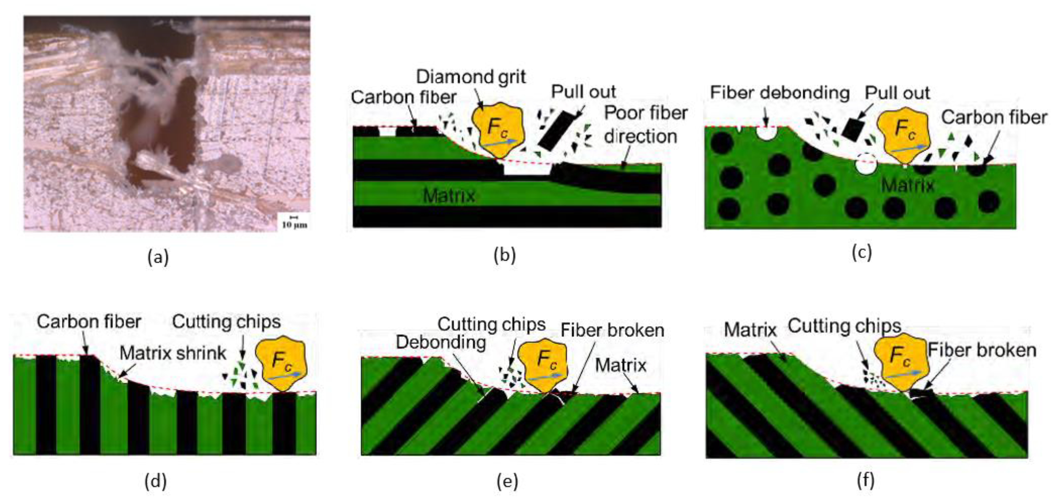
6. Material Removal Mechanism of Dicing Blades

In addition to the primary removal mechanism, a few recommendations in the literature for improving the material removal process provide a clear understanding of the cutting mechanism via dicing blades. The dicing blade material removal process varies based on the morphology of the workpiece. To begin with carbon-fiber-reinforced plastic (CFRP) composites, plastic flow in the local regions of fibers and resins, along with micro breakage, was identified as the primary material removal mechanism. Furthermore, macroscopic and microscopic simulations are suggested for gaining a better understanding of the CFRP composite cutting mechanism [48]. Likewise, plastic flow is responsible for cutting in the grinding of brittle materials [58]. For composite materials, the material removal process changes as the fiber orientations change, as shown in Figure 12b–f. If the dicing direction is parallel to the fiber orientation, the scratching action takes advantage of improper fiber embedding in the matrix [48]. A perpendicular dicing direction to fiber orientation, on the other hand, proceeds the cutting action with a diamond grit tip owing to the small cutting depth and proper fixation of carbon fibers in the matrix, resulting in a smooth surface finish. Dicing at an angle causes visible fiber breakage due to delicate support and extreme cutting force applied by diamond grits. For the cutting process with silicon, three material removal steps are responsible: rubbing, plastic deformation, and cracking, whereas for alumina, intergranular and transgranular mechanisms play a role [45].
Numerical simulations for sapphire substrates revealed that the plowing action caused by the grinding particles and sinter was a significant factor in material removal. Figure 12a depicts the side topography of the cutting groove in aramid fiber-reinforced plastic (AFRP) composites; due to the higher toughness of aramid fibers, peeling instead of cutting results in a small number of burrs on the cutting groove edges [52]. The cutting mechanism of AFRP composites can be improved by using abrasive particles with cutting edges smaller than the diameter of the aramid fibers, which reduces damages caused by tool size and corresponding cutting speed.

7. Applications of Dicing Blades

Dicing blades replace traditional cutting methods to achieve close tolerances in workpiece profiling. Its contribution is examined with the potential for new research frontiers in the following subsections.

7.1. Machining of Hard-to-Cut Materials

Material-to-material analysis of cutting dicing blades provides an overview of influential machining parameters and associated factor relationships that affect the machined surface. To begin, silicon (Si) was a prominent material that served as an input material in many microelectronic industries where precision dicing and grinding had been traditionally used for fragile materials. Wear mechanisms and machining of silicon wafer dicing were investigated [59,60], and two stages were identified as steady and transient [61,62]. The coefficient of friction and rate of wear are higher in the transient stage than in the steady state, but differentiating between the two stages is difficult. After that, a methodology for evaluating the wear coefficient and stage of wear at a particular point in time was developed [63]. Surface roughness can be determined by factors such as cooling water temperature, feed speed, and rotational speed; roughness values become consistent regardless of variable grit sizes in the steady stage, whereas roughness values increased sharply for two grit sizes in the transient stage (cutting distance 0–300 m), as shown in Figure 13. Furthermore, three dicing blade features were tested using variable grit sizes, exposure lengths, and thickness, and it was noticed that smaller-grit-size blades exhibit stable chipping widths [64]. Aside from individual factors, the relationships between factors could be established, such as a direct relationship between dicing forces and workpiece feed rate and an inverse relationship between spindle rotational speed and dicing force [53]. It was found that wafer chipping increases with the feed rate of the workpiece whereas it decreases as the rotational speed increases [65]. Additionally, optimal dicing conditions of higher rotational speed and lower feed rate produce lesser dicing forces.
A high-speed microcutting method was proposed for CFRP composites that are difficult to cut with traditional methods due to a lack of homogeneity and anisotropic behavior [48]. The method examines two types: metal- and resin-bonded blades’ performance for surface quality, and as a result, metal-bonded blades gain preference over resin-bonded blades. Another aspect surfaced about the surface morphology of diced CFRP composites that are fiber-orientation-dependent: for 0° orientations, fibers are cut along the axis, leaving few unparalleled fibers on the surface of the substrate. On the contrary, at 90°, cutting of fiber takes place smoothly due to the strong fixation of fibers in the matrix represented in Figure 14a-h. To be used in the aerospace industry, CFRP composites are mixed with AFRP composites, and despite minimizing major defects with traditional methods such as milling [66], laser cutting [67], and ultrasonic [68] and waterjet cutting [69], the cost of processing needs to be reduced further [52]. For that machining alternate, an ultrathin diamond dicing blade with a cutting edge much smaller than the diameter of the AFRP composite fiber, as shown in Figure 15, proved useful. After assessing the effects of cutting force, temperature, and spindle current on surface roughness, cutting speed was found to be the most influential parameter, with feed speed having a moderate effect and cutting depth being the least effective.
The high-speed machining process of quartz and graphite with dicing blades is influenced by strain rate and dynamic diameter [70,71]. To determine the relationship between machining parameters and dynamic diameter, the impact of variable parameters such as rotational speed, static diameter, and elastic modulus of blades was also considered [70]. As a result, both theoretically and experimentally, a direct relationship between dynamic diameter and rotational speed was discovered, indicating a positive correlation between dynamic diameter and machining precision, as illustrated in Figure 16. Furthermore, the dynamic diameter increases slightly in theoretical calculations that exclude diamonds compared to calculations that include diamonds. For quartz, a widely used optical substrate, the strain rate is related to the linear velocity of diamond blades and is affected by linear velocity, feeding speed, diameter, dicing depth, diamond blade density, and the elastic modulus of quartz glass [71]. Hardening and heat generation were identified as major causes of concern at high dicing speeds after analyzing the effects of the high strain rate in quartz dicing.
Sapphire and dielectric substrates in the manufacture of light-emitting diodes (LEDs) require chip-free grooves during sapphire cutting, which is difficult to achieve with traditional dicing blades. Three blades were made to produce ultrafine grooves: one with nickel-phosphorus alloy and the other with vitric material [72]. Dense traditional blades (orientation-dependent) generate meandering lines and break after a certain cutting length, as shown in Figure 17a, whereas fabricated blades are sapphire-orientation-independent and have a greater cutting ability, as shown in Figure 17b. The gradual wear of diamonds in sapphire cutting while exposing fresh diamonds for machining is the reason for increased cutting capacity. Likewise, an ultrathin dielectric substrate of lithium niobate (LiNbO3) can be separated by a precise dicing operation [73].
Figure 18a depicts the machining of optical materials such as lithium niobate, YAG, silicon, and germanium using typical dicing machines [74]. Ductile dicing cuts through plastic deformation of chips caused by tool parameters such as shape, material, and rotational speed, as well as other parameters such as diamond size concentration, sample translation speed, depth of cut, and coolant. Figure 18b shows that dicing germanium produces a smooth surface with no chipping or pitting, whereas dicing YAG produces a rough surface with some pitting but no cracking or chipping as shown in Figure 18c. Furthermore, Figure 18d shows that lithium niobate has little pitting but no cracking or chipping, whereas silicon has some cracking or chipping visible in Figure 18e. Another contribution of dicing blades in crystalline materials of lithium niobate and garnets for obtaining high-quality optical-grade surfaces is the generation of low coupling loss to produce facets in silica on silicon [75]. Additionally, the optimal process parameters for rotational and translational speeds for flame hydrolysis deposition (FHD) silica on silicon planar substrate can be determined.
A diamond abrasive blade develops the parametric relations for high alumina by changing the process parameters of feed speed, blade rotation (w), and depth of cut [45]. Blade wearing is higher at lower feed rates and increased rotational speed of the blade for all cutting depths and rotational speeds analyzed, as shown in Figure 19a. The effect of three parameters, dicing speed, dicing saw preprocessing, and dual dicing blade, on chip strength in silicon wafers shows that dual dicing increased chip strength by 15% and the new blade without dressing yielded a 61% reduction in chip strength, while a 50% reduction in dicing speed yielded an almost 13% increase in chip strength, as shown in Figure 19b [76].
By keeping the cutting length constant and measuring the roughness types (Ra and Rz), metal-bonded dicing blades with grit sizes of 5 and 30 µm revealed the effect of blade wear and sidewall quality for monocrystalline Si and SiC ceramic (SSiC) [77]. Ra was found to be undetermined for Si and SSiC, whereas Rz decreases as cutting length increases. By machining third-generation material SiC for the formation of blue-ray and laser diodes, resin-bonded blades performed better than metal-bonded blades, effectively reducing chipping fracture, which otherwise grows enormously [54]. Chipping and kerf width increase sharply with increasing cutting depth for sintered metal-bonded blades [78]. Furthermore, ceramic materials were diced to investigate the structural integrity of nickel-bonded diamond blades in terms of tool wear and surface roughness, and a confocal microscope and SEM were used to analyze wear and surface roughness, respectively [79].

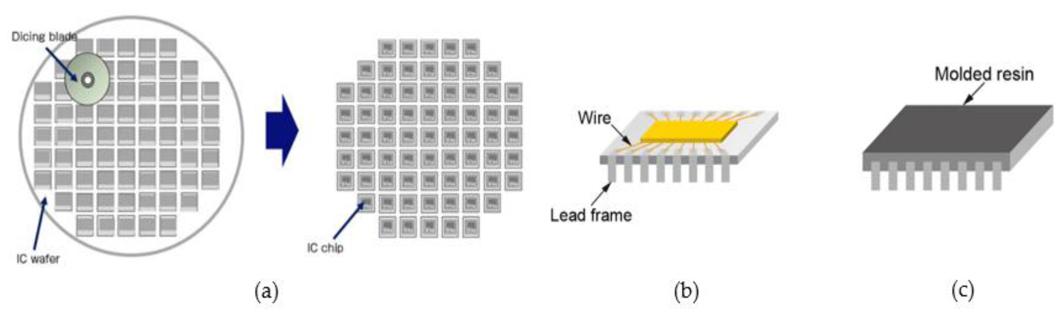
7.2. Back-End Process of IC

The manufacturing of semiconductors is completed by a three-phase design, front- and back-end [80,81]. The back-end process typically separates the integrated circuit into individual chips, and the front-end process creates large-scale circuits on silicon wafers. The back-end is further divided into three stages: dicing, wire bonding, and molding, as shown in Figure 20. Rotating circular diamond dicing blades cut each wafer on predefined dicing lines depicted in Figure 20a while attached to dicing tape and sprayed with ultrapure water. Because the stretching of the tapes after dicing provides clearance between the chips for removal, dicing tape must be unaffected during cutting. Because worn dicing blades cause chipping, smooth edges are required after dicing: roughness values must remain within allowable limits to prevent the part from failing. A lead frame that acts as a thin metal support and provides a terminal for placing the semiconductor on board is used to fix chips in the wire bonding process (die bonding) shown in Figure 20b. As shown in Figure 20c, thin gold wires connect the chips to the lead frame during the wire bonding process and then complete the encasing of the chips in the epoxy resin during the molding phase.

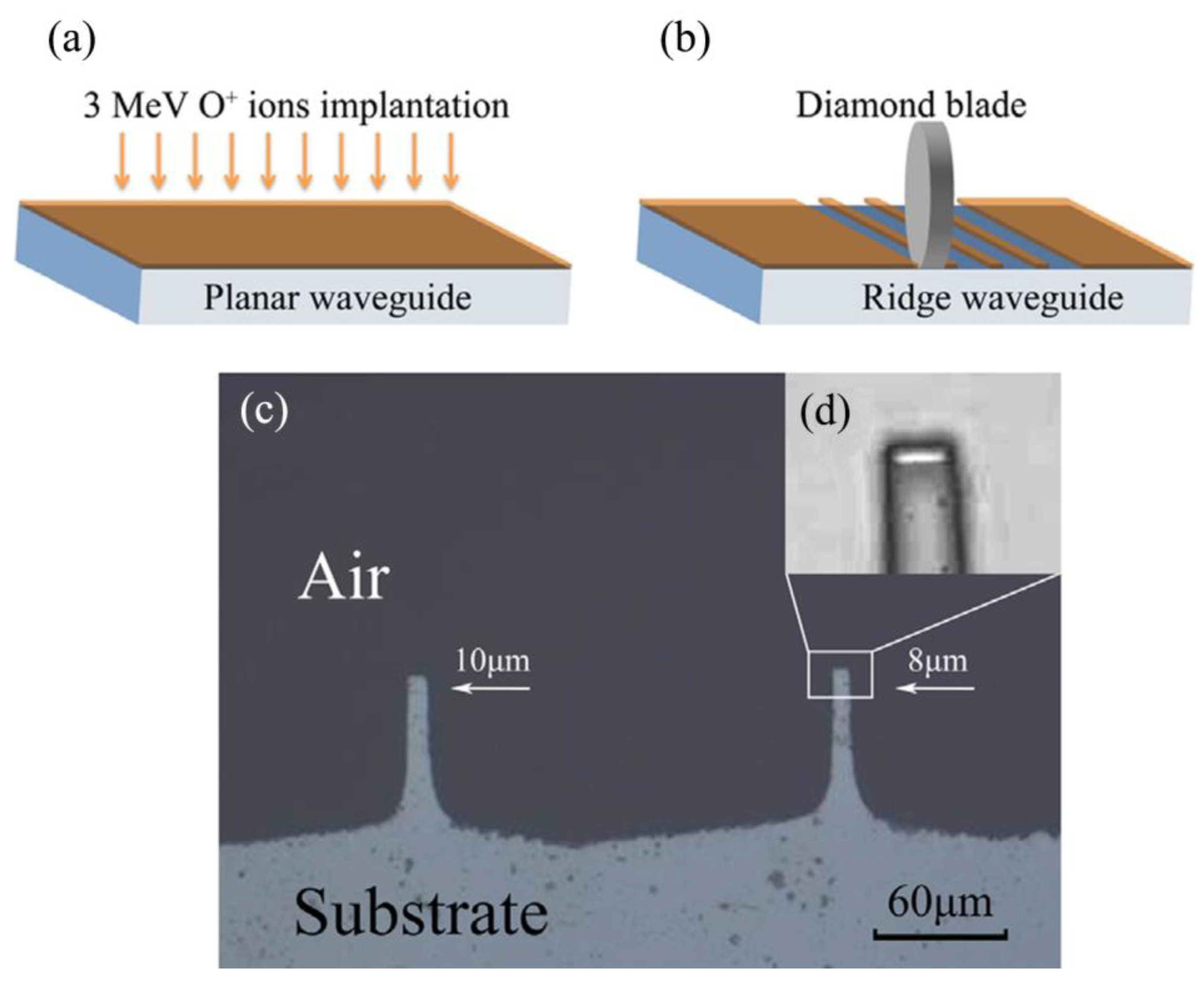
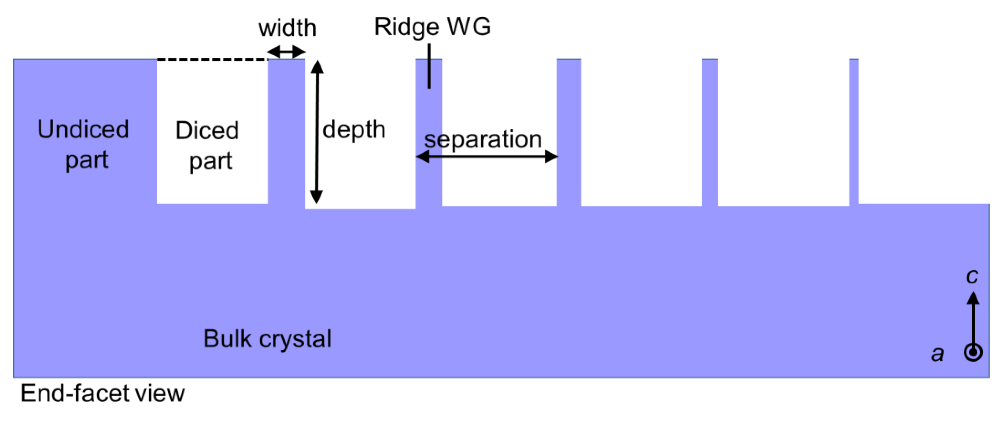
7.3. Optical Waveguide Formation

Blade dicing is a popular secondary technique used to form waveguides in nonlinear multifunctional optical crystals, mid-infrared disordered crystals, rare-earth ion-doped disordered laser crystals, and piezoelectric materials. Optical waveguides that are a few micrometers in diameter contribute to optical information processing [82]. The level of propagation loss after waveguide processing determines how well the waveguide surface will operate in actual situations and is affected by chipping produced by dicing [83]. Ridge waveguides outperform planar structures in optics when it comes to focusing light field energy in two directions [84,85]. Such benefits include higher density applicable for high-density optical data storage [86].
Applying a 1D surface waveguide layer to a target optical material first and then removing specific parts of the target material can form 2D light-emitted waveguides [85,87,88]. To create a 1D waveguide surface, the primary step contains procedures such as ion irradiation/implantation [89,90,91,92,93], femtosecond laser inscription [94], ion exchange [43], and metal diffusion [95]. The majority of researchers created planar and ridge waveguides in optical materials using blade dicing in conjunction with the ion exchange approach [96,97,98]. In terms of materials, the role of dicing blades in the formation of ridge waveguides is discussed further below.
In nonlinear optics and advanced photonics, lithium niobate (LiNbO3) becomes important due to its electro-optic and acousto-optic properties [99]. Ion implantation and precise diamond blade dicing produce ridge waveguides with a depth of 40 µm and widths of 8 and 10 µm on the planar waveguide surface, as shown in Figure 21, thanks to the optimal process parameters for chip- and crack-free surfaces. The bright horizontal zone at the top of the structure cross-section shows the ridge waveguide in Figure 21d; the propagation loss of the 8 µm wide ridge waveguide was 2.2 dB/cm after annealing. The same combination of O5+ ion irradiation and precise diamond blade dicing gave the ridge waveguide in mid-infrared wavelength for MgO:LiNbO3 crystals [100]. Thermal annealing improves waveguide guiding capacity and reduces propagation losses to as low as 1.0 dB/cm. For crystals of zinc selenide (ZnSe), two ridge waveguides widths of 20 µm and 50 µm gave a propagation loss of 1.1 dB/cm by implementing the swift Kr8+ ion irradiation and precise diamond blade dicing combination [101]. Similarly, in the crystals of neodymium-doped calcium-niobium-gallium-garnet (Nd:CNGG), the ridge waveguide gave a propagation loss of 3.8 dB/cm by controlling the distance between adjacent grooves [102].
The combination of carbon ion irradiation and precise diamond blade dicing also fulfills the optical requirements of piezoelectric and rare-earth ion-doped materials through ridge waveguides [103,104]. For instance, lanthanum gallium silicate (La3Ga5SiO14 or LGS), a profound piezoelectric material that possesses outstanding properties of a relatively high electromechanical coupling coefficient and allows the development of new-generation miniature communication devices, was taken to form two high-quality ridge waveguides with propagation losses of 1.6 dB/cm at 632.8 nm and 1.2 dB/cm at 1064 nm wavelengths [104]. Likewise, rare-earth ion-doped disordered laser crystals (Nd:SrLaGa3O7 and Nd:SrGdGa3O7) served as a potential substrate to form ridge waveguides ending with the minimized propagation loss of 1 dB/cm, but substrate samples underwent an annealing process for the reduction in defects surfaced during the ion irradiation process [103]. Computer programs facilitate the maneuvering of groove width, depth, and distance between two adjacent grooves during waveguide formation.
A ridge waveguide with a width of 25 µm was formed between two neighboring grooves in neodymium-doped yttrium calcium oxyborate Nd:YCa4O(BO3)3, (Nd:YCOB) [105], Nd:GdCOB [106], and YCOB nonlinear optical crystals [107] by combining carbon ion irradiation and precise diamond blade dicing processes. Optimal dicing parameters lessen the chipping and cracking on the edges of the groove. The fabricated waveguide was polarization-dependent and, for planar and ridge waveguides, propagation losses calculated were 8 dB/cm and 7 dB/cm, respectively [105]. The same C5+ ion irradiation and blade dicing combination were used to fabricate ridge waveguides in lithium fluoride crystals with minimal propagation losses: 0.7 dB cm−1 at 1064 nm, 0.4 dB cm−1 at 2200 nm, and 0.4 dB cm−1 at 4000 nm wavelength [108]. H+ ion implantation and precise diamond blade dicing formed the ridge waveguides in high-gain Nd3+-doped laser glass [86]. End-face coupling provides optical confinement for the ridge waveguide, and its propagation loss at 976 nm was 3.9 dB/cm.
A combination of blade dicing saw and Rb exchange fabricates ridge waveguides in z-cut potassium titanyl phosphate (KTP) [109]. It was found that high-energy accelerators can be avoided in the case of the ion implantation technique to gain smaller widths of the waveguide. The surface produced a lower surface roughness that allows for low losses and acceptable quality for diced ridge sidewalls with a propagation loss of 1.3 dB/cm at a 1550 nm wavelength. An optical waveguide was formed in high-gain laser material, Yb3+-doped silicate glass, where diamond blade dicing created parallel air grooves on a planar waveguide and the end-face coupling technique gave a propagation loss of 3.20 dB/cm [110]. Furthermore, a diamond saw utilized ridge waveguides to achieve deep dicing, i.e., high aspect ratios in channels (waveguides) on Tm3+: LiYF4 fluoride crystals [111] and ytterbium-doped calcium fluoride crystals [112]. Figure 22 shows a precision dicing blade that manufactures surface channels with a depth of 200 m along the c-axis and variable widths of 10 to 50 m with a step of 10 m. To improve the quality of end facets, vertical surfaces were produced by cutting material orthogonally to the ridge. Propagation losses for diced channels range from 0.20 to 0.43 dB/cm with the limitation of thermal issues associated with power scaling, which somehow can be addressed by active cooling. Through dicing trenches, high-quality crack-free silicon nitride waveguides with propagation losses less than 0.5 dB/cm can be produced [113].
The preceding discussion establishes the importance of precision dicing blades in the fabrication of ridge waveguides in a variety of materials. By combining precise diamond blade dicing with ion implantation/irradiation, low propagation losses can be achieved. These findings lay the groundwork for future research into whether other materials in the same category can benefit from the combination of precise diamond blade dicing and ion implantation.

7.4. Surface Micro Texturing

The dicing process entices researchers with micropatterns generated on difficult-to-cut materials for its widespread application. For example, diced edges provide less edge chipping and sidewall roughness than sawn edges, which are critical in the machining of SiC substrates illustrated in Figure 23a,b [114]. Ceramic substrates had a better edge surface after dicing than monocrystalline substrates, which had visible traces of grain on the surface depicted in Figure 23c,d. For alumina, qualitative chipping analyses revealed lower levels; following that, two groups with different cutting parameters were observed for their surface roughness: the first group preserved more edges with an even distance between cuts as depicted in Figure 23e,f, while the second group revealed severe intergranular fractures with an uneven distance between cuts as shown in Figure 23g,h [45]. To create a fine surface finish on optical materials, ductile-mode dicing adopted optimal processing parameters for samples with surface metrology of 15 × 15 µm [74]. Results revealed that lower surface roughness can be achieved for optical materials: 2.1 nm for germanium without defects, 3.5 nm for YAG with minor defects, 7.9 nm for lithium niobate with some defects, and 8.6 nm for silicon with pitting of order 0.5–2 µm, shown in Figure 24a–d.

8. Summary and Future Outlook

Taken together, this paper explains the advantages of using dicing blades, in particular, to machine hard-to-cut and optical materials, which are less likely to be achieved using traditional machining processes (water jet, laser, electrochemical machining, and electric discharge machining). A template for precision is generated by a thorough assessment of the evidence by discussing and analyzing methods for the accuracy and precision of the manufactured part. Dicing blade performance is evaluated in terms of its ability to produce microstructures with lesser dicing defects and enhanced workpiece surface characteristics.
  • The prominent key points are:
    • Dicing blades are capable of forming microstructures on materials such as SiC, quartz, silicon, alumina, CFRP composites, AFRP composites, optical materials, and ceramics while addressing issues such as chipping, cracking, surface roughness, and cutting-edge quality. But besides incorporating optimal dicing and machining parameters for dicing blades, strain rate and dynamic diameter may still influence the surface quality and tolerances.
    • The combination of ion irradiation and precise diamond blade dicing shows an efficient method for fabricating high-quality ridge waveguides with lower propagation losses in optical materials, which leads to an increase in waveguide guiding capacity.
    • To address dicing defects, optimization techniques create a compatible microstructure on materials to be used in devices (MEMSs and ICs). For example, intervention during the dicing blade preparation phase includes the addition of photopolymerizable resins, BEO, and whisker, which improves machinability, hardness, and wear resistance and reduces chipping and cracking. Furthermore, changes in matrix composition result in a lower unit chipping coefficient, while truing and laser dressing produce sharp grooves and cutting edges. Interventions at the dicing technique level include on-machine laser dressing, which improves surface roughness while allowing for in-line detection of cutting defects. Furthermore, the dual dicing scheme avoids larger cutting groove angles, and PCD blades ensure better surface quality with less chipping.
  • Combining the appealing properties of dicing blade machining with recent advances can envision new research benchmarks, including but not limited to the following:
    • In the context of optical materials, research can be conducted on the path of single-mode transmissions to further reduce propagation losses. To produce waveguides with high quality and low loss, the fabrication conditions of proton implantation and precise diamond blade dicing should be optimized in the future. For nonlinear frequency conversion, the possibility of fabricating quasi-phase-matching (QPM) ridge waveguides in z-cut KTP through the use of Rb exchange and diamond blade dicing saw may be explored.
    • The concept of dual dicing can be explored further for multilayer specimen materials such as low-temperature cofired ceramic (LTCC) and PZT (lead zirconate titanate).
    • Keeping in mind the effect of the dynamic diameter of the dicing blade on precision machining, other factors such as dynamic inner diameter and Young’s modulus of the dicing blade require further investigation.
    • Future research may include testing a broader range of materials using recognized optimization techniques and numerical modeling of the dicing process for verification purposes.

Author Contributions

Conceptualization, Z.Y.; methodology, A.R.; formal analysis, A.R.; investigation, A.R.; writing—original draft preparation, A.R. and B.s.C.; writing—review and editing, A.R.; visualization, B.s.C.; supervision, Z.Y.; project administration, Z.Y.; funding acquisition, Z.Y. All authors have read and agreed to the published version of the manuscript.

Funding

This research was funded by the National Natural Science Foundation of China, China (grant number 52275455), Liaoning Revitalization Talents Program, China (grant number XLYC2007133), and Natural Science Foundation of Liaoning Province, China (grant number 2020-MS-213).

Data Availability Statement

Not applicable.

Acknowledgments

This paper is supported by the National Natural Science Foundation of China, China (grant number 52275455), Liaoning Revitalization Talents Program, China (grant number XLYC2007133), and Natural Science Foundation of Liaoning Province, China (grant number 2020-MS-213). We thank the associate editor and the reviewers for their useful feedback, which improved this paper.

Conflicts of Interest

The authors declare no conflict of interest.

References

  1. Von Witzendorff, P.; Stompe, M.; Suttmann, O.; Rissing, L.; Overmeyer, L. Investigation of the cutting performance of laser dressed metal bonded diamond blades. Intl. Cong. App.L. Elect.Opt. 2013, 2013, 840–845. [Google Scholar]
  2. Deng, H.; Xu, Z. Laser-dressing topography and quality of resin-bonded diamond grinding wheels. Opt. Lasers Eng. 2021, 136, 106322. [Google Scholar] [CrossRef]
  3. Han, W.; Kunieda, M. Precision electrochemical machining of tungsten micro-rods using wire electrochemical turning method. Int. J. Adv. Manuf. Technol. 2020, 111, 295–307. [Google Scholar] [CrossRef]
  4. Miao, X.; Qiang, Z.; Wu, M.; Song, L.; Ye, F. The optimal cutting times of multipass abrasive water jet cutting. Int. J. Adv. Manuf. Technol. 2018, 97, 1779–1786. [Google Scholar] [CrossRef]
  5. Mizuno, M.; Iyama, T.; Zhang, B. Analysis of the sawing process with abrasive circular saw blades. J. Manuf. Sci. Technol. 2008, 130. [Google Scholar] [CrossRef]
  6. Efrat, U. Optimizing the wafer dicing process. In Proceedings of the 15th IEEE/CHMT International Electronic Manufacturing Technology Symposium, Santa Clara, CA, USA, 4–6 October 1993. [Google Scholar]
  7. Principles of Dicing. Available online: https://www.inseto.co.uk (accessed on 13 November 2022).
  8. 061127-Dicing Saw (Dicing Saw, Blade) PPT. Available online: https://wenku.baidu.com (accessed on 18 May 2022).
  9. Shen, J.; Zhu, X.; Chen, J.; Tao, P.; Wu, X. Investigation on the Edge Chipping in Ultrasonic Assisted Sawing of Monocrystalline Silicon. Micromachines 2019, 10, 616. [Google Scholar] [CrossRef]
  10. Sullivan, S. Dicing of MEMS Devices. In Handbook of Silicon Based MEMS Materials and Technologies, 1st ed.; Elsevier: Oxford, UK, 2010; pp. 601–606. [Google Scholar]
  11. Martin, D.; Sullivan, S. Dicing of MEMS Devices. In Handbook of Silicon Based MEMS Materials and Technologies, 2nd ed.; Elsevier: Oxford, UK, 2015; pp. 671–677. [Google Scholar]
  12. Plasma Dicing 101: The Basics. Available online: https://www.kla.com (accessed on 13 November 2022).
  13. Precision Processing Tools. Available online: https://www.disco.co.jp/eg/support/term/doc/PrecisionProcessingTools.pdf. (accessed on 13 May 2022).
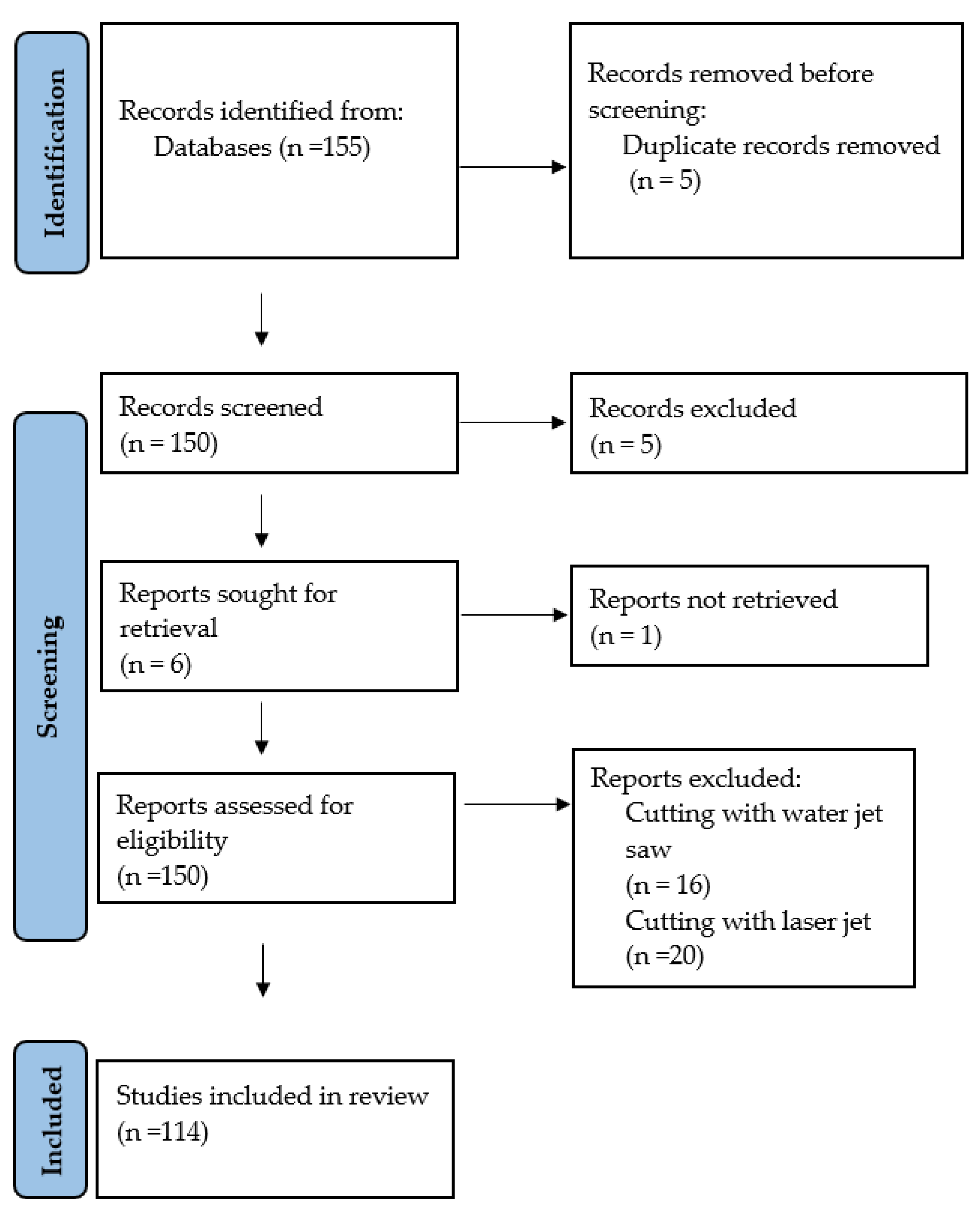
  14. Liberati, A.; Altman, D.G.; Tetzlaff, J.; Mulrow, C.; Gøtzsche, P.C.; Ioannidis, J.P.; Clarke, M.; Devereaux, P.J.; Kleijnen, J.; Moher, D. The PRISMA statement for reporting systematic reviews and meta-analyses of studies that evaluate health care interventions: Explanation and elaboration. J. Clin. Epidemiol. 2009, 62, e1–e34. [Google Scholar] [CrossRef]
  15. Yuan, Z.; Feng, S.; Wu, T. Preparation and characterization of ultra-thin dicing blades with different bonding properties. Int. J. Adv. Manuf. Technol. 2022, 119, 1–16. [Google Scholar] [CrossRef]
  16. Yuan, Z.; Cheng, K.; Zhang, Y.; Hu, J.; Zheng, P. Investigation on the fabrication of dicing blades with different sintering methods for machining hard-brittle material wafers. Proc. Inst. Mech. Eng. Pt. B J. Eng. Manuf. 2019, 233, 1781–1793. [Google Scholar] [CrossRef]
  17. Selecting Right Diamond Dicing Blade for Your Application. Available online: https://www.ukam.com (accessed on 13 May 2022).
  18. Creating Man-Made Diamonds. Available online: https://d.neadiamonds.com (accessed on 2 February 2023).
  19. Lab-Grown Diamond Production Methods. Available online: https://www.gemsociety.org (accessed on 2 February 2023).
  20. Wang, J.; Zhao, Q.; Zhang, C.; Guo, B.; Yuan, J. Arc envelope grinding of sapphire steep aspheric surface with sic-reinforced resin-bonded diamond wheel. Int. J. Prec. Eng. Manuf. G. Technol. 2021, 8, 1083–1094. [Google Scholar] [CrossRef]
  21. Monteverde, F. Hot pressing of hafnium diboride aided by different sinter additives. JMatS 2008, 43, 1002–1007. [Google Scholar] [CrossRef]
  22. Yu, Z.; Zhao, P.; Hu, F. Study on UV Curing Behavior and Properties of ES/CEP Resin. Cai. Dao./Mat. Rev. 2018, 32, 263–267. [Google Scholar]
  23. Gild, J.; Kaufmann, K.; Vecchio, K.; Luo, J. Reactive flash spark plasma sintering of high-entropy ultrahigh temperature ceramics. Scripta Mater. 2019, 170, 106–110. [Google Scholar] [CrossRef]
  24. Song, S.-X.; Wang, Z.; Shi, G.-P. Heating mechanism of spark plasma sintering. Ceram. Int. 2013, 39, 1393–1396. [Google Scholar] [CrossRef]
  25. Cho, H.J.; Yan, D.; Tam, J.; Erb, U. Effects of diamond particle size on the formation of copper matrix and the thermal transport properties in electrodeposited copper-diamond composite materials. JAllC 2019, 791, 1128–1137. [Google Scholar] [CrossRef]
  26. Stompe, M.; Cvetkovic, S.; Taptimthong, P.; Rissing, L. Ultra-precision Dicing Process Separation: Effect of Circumferential and Sidewall Grinding. In Proceedings of the 12th euspen International Conference, Stockholm, Sweden, 4–8 June 2012. [Google Scholar]
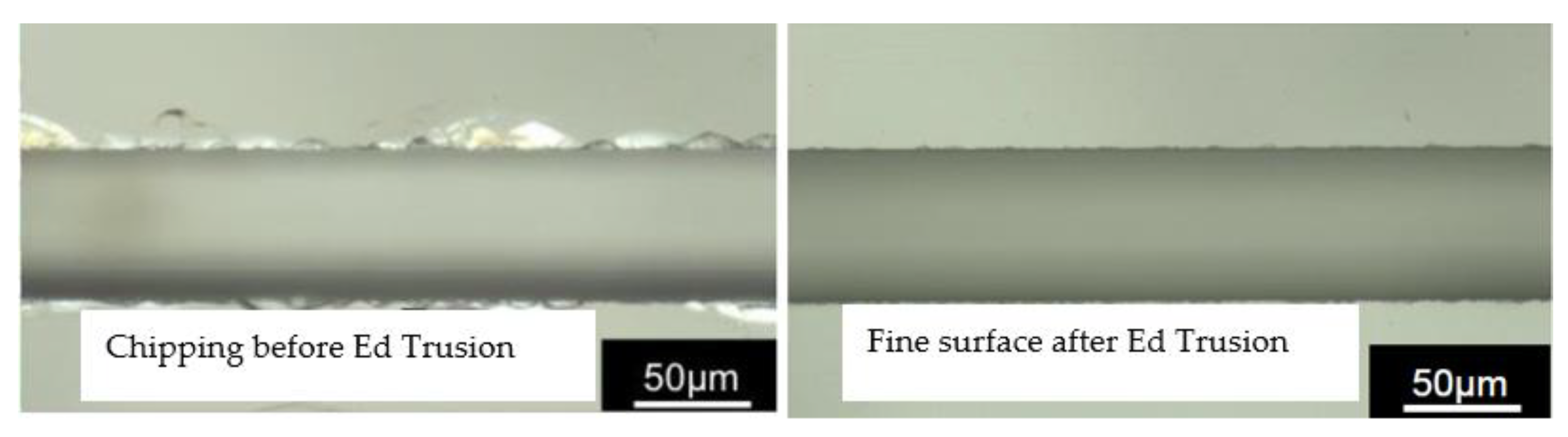
  27. Watanabe, K.; Yanagida, D.; Minami, H.; Izumi, Y. Electrical discharge truing of a PCD blade tool on a dicing machine. Procedia CIRP 2020, 95, 494–498. [Google Scholar] [CrossRef]
  28. Shi, K.W.; Yow, K.; Khoo, R. Developments of blade dressing technique using SiC board for C90 low-k wafer sawing. In Proceedings of the 13th Electronics Packaging Technology Conference, Singapore, 7–9 December 2011. [Google Scholar]
  29. Von Witzendorff, P.; Moalem, A.; Kling, R.; Overmeyer, L. Laser dressing of metal bonded diamond blades for cutting of hard brittle materials. JLasA 2012, 24, 022002. [Google Scholar] [CrossRef]
  30. Von Witzendorff, P.; Stompe, M.; Moalem, A.; Cvetkovic, S.; Suttmann, O.; Overmeyer, L.; Rissing, L. Dicing of hard and brittle materials with on-machine laser-dressed metal-bonded diamond blades. Prec. Eng. 2014, 38, 162–167. [Google Scholar] [CrossRef]
  31. Stompe, M.; Witzendorff, P.; Cvetkovic, S.; Moalem, A.; Stute, U.; Rissing, L. Concept for performance-enhancement of ultra-precision dicing for bulk hard and brittle materials in micro applications by laser dressing. MiEng 2012, 98, 544–547. [Google Scholar] [CrossRef]
  32. Stompe, M.; Cvetkovic, S.; Taptimthong, P.; Rissing, L. Dressing Criteria for Inline Laser Dressing of Metal-bonded Dicing Blades. In Proceedings of the 12th euspen International Conference, Stockholm, Sweden, 4–8 June 2012. [Google Scholar]
  33. Chu, J.; Lai, B.-Z.; Yiu, P.; Shen, Y.-L.; Chang, C.-W. Metallic glass coating for improving diamond dicing performance. Sci. Rep. 2020, 10, 1–10. [Google Scholar] [CrossRef]
  34. Hishamuddin, M.I.; Nayan, N. Reverse Engineering of Dicing Blade to Prolong its Lifetime. Evol. Elect. Electr. Eng. 2020, 1, 161–166. [Google Scholar]
  35. Deng, J.; Zhang, J.; Tu, Y.; Yang, P.; An, M.; Wang, P. Effect of BEO in the electrodeposition process of Ni/diamond composite coatings for preparation of ultra-thin dicing blades: Experiments and theoretical calculations. Ceram. Int. 2018, 44, 16828–16836. [Google Scholar] [CrossRef]
  36. Zhu, X.; Wang, Y.; Liu, J.; Wang, Z.; Dong, F. Research of diamond concentration in dicing blade effect by electroplating parameter. In Proceedings of the International Conference on Advanced Composite Materials and Manufacturing Engineering, Yunnan, China, 22–23 June 2019. [Google Scholar]
  37. Peng, W.; Xu, X.; Zhang, L. Improvement of a dicing blade using a whisker direction-controlled by an electric field. J. Mater. Process. Technol. 2002, 129, 377–379. [Google Scholar] [CrossRef]
  38. Lee, S.; Tani, Y.; Enomoto, T.; Sato, H. Development of a dicing blade with photopolymerizable resins for improving machinability. CIRP Ann. 2005, 54, 293–296. [Google Scholar] [CrossRef]
  39. Fujita, T.; Izumi, Y.; Watanabe, J. Ultra-fine grooving technology with high aspect ratio for cemented carbide by PCD (poly-crystalline diamond) blade. Prec. Eng. 2019, 55, 381–389. [Google Scholar] [CrossRef]
  40. Fujita, T.; Izumi, Y.; Watanabe, J. Ultrafine ductile-mode dicing technology for SiC substrate with metal film using PCD blade. J. Adv. Mech Des. Syst. Manuf. 2019, 13, 1–14. [Google Scholar] [CrossRef]
  41. Stompe, M.; Cvetkovic, S.; Rissing, L. Dicing concept for mechanical structured materials and multi- layer-specimens. In Proceedings of the 13th euspen International Conference, Berlin, Germany, 27–31 May 2013. [Google Scholar]
  42. Jiun, H.; Ahmad, I.; Jalar, A.; Omar, G. Effect of Laminated Wafer Toward Dicing Process and Alternative Double Pass Sawing Method to Reduce Chipping. Electr. Pack. Manuf. IEEE Trans. 2006, 29, 17–24. [Google Scholar] [CrossRef]
  43. Tervonen, A.; Honkanen, S.K.; West, B.R. Ion-exchanged glass waveguide technology: A review. Opt. Eng. 2011, 50, 071107. [Google Scholar]
  44. Ikeno, J.; Tani, Y.; Fukutani, A.; Sato, H. Development of chipping-free dicing technology applying electrophoretic deposition of ultrafine abrasives. CIRP Ann. 1991, 40, 351–354. [Google Scholar] [CrossRef]
  45. Araujo, L.; Foschini, C.; Jasinevícius, R.; Fortulan, C. Precision dicing of hard materials with abrasive blade. Int. J. Adv. Manuf. Technol. 2016, 86, 2885–2894. [Google Scholar] [CrossRef]
  46. Cheung, A.T. Dicing advanced materials for microelectronics. In Proceedings of the International Symposium on Advanced Packaging Materials: Processes, Properties and Interfaces, Irvine, CA, USA, 16–18 March 2005. [Google Scholar]
  47. Perrottet, D.; Durrant, P.; Richerzhagen, B. Water-jet-guided Laser Technology: A Damage-free Dicing Solution. Adv. Pack. 2006, 15, 24. [Google Scholar]
  48. Yuan, Z.; Hu, J.; Wen, Q.; Cheng, K.; Zheng, P. Investigation on an Innovative Method for High-Speed Low-Damage Micro-Cutting of CFRP Composites with Diamond Dicing Blades. Materials 2018, 11, 1974. [Google Scholar] [CrossRef] [PubMed]
  49. Zhang, Z.; Yang, X.; Zheng, L.; Xue, D. High-performance grinding of a 2-m scale silicon carbide mirror blank for the space-based telescope. Int. J. Adv. Manuf. Technol. 2017, 89, 463–473. [Google Scholar] [CrossRef]
  50. Li, M.-C.; Zhang, F.-L.; Zhou, Y.-M.; Li, W.-X.; Wu, S.; Wu, S. Preparation and performance of resin-bonded grinding wheel with braze-coated diamond grits. DRM 2020, 101, 107619. [Google Scholar] [CrossRef]
  51. Su, Z.; Zhang, S.; Wu, J.; Liu, L.-L. Cutting performance evaluation of nickel-plated graphite Fe-based diamond saw blades. DRM 2021, 114, 108344. [Google Scholar] [CrossRef]
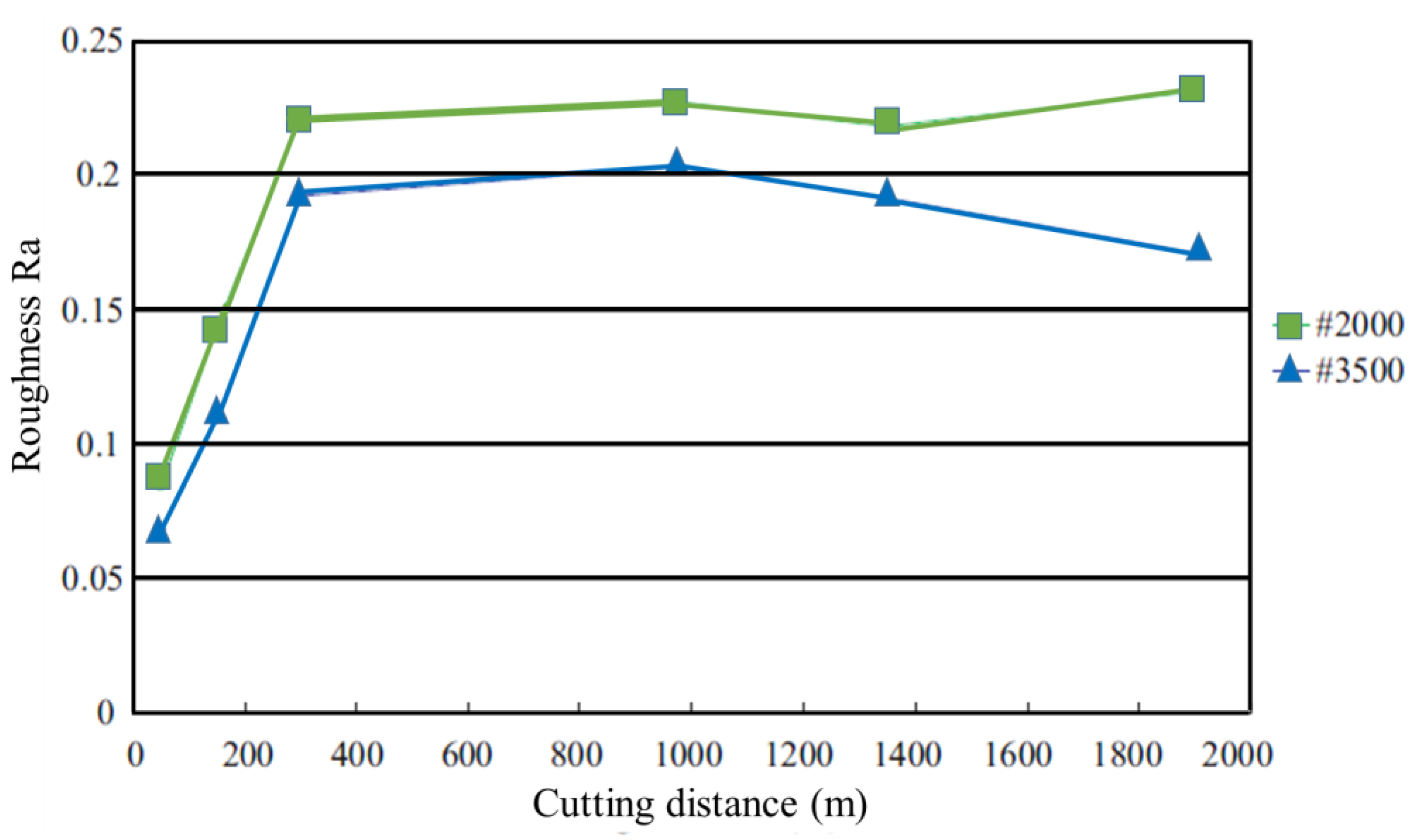
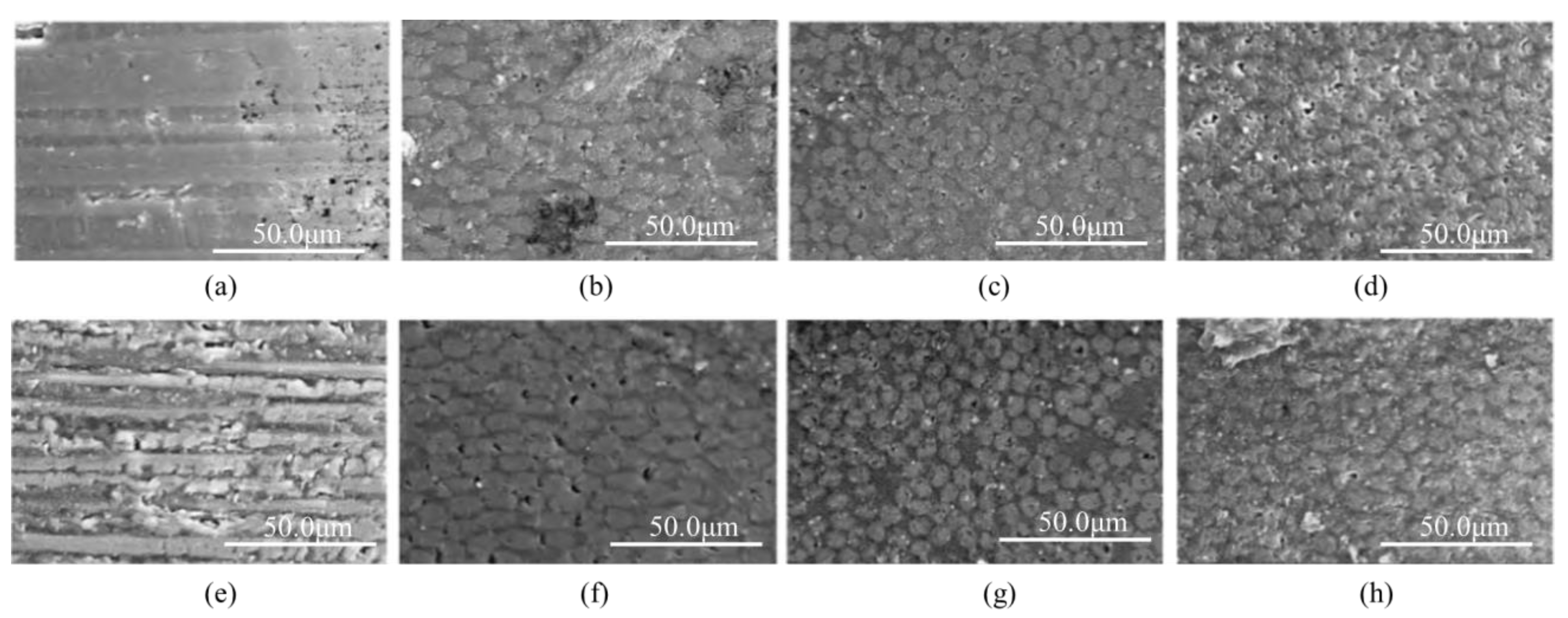
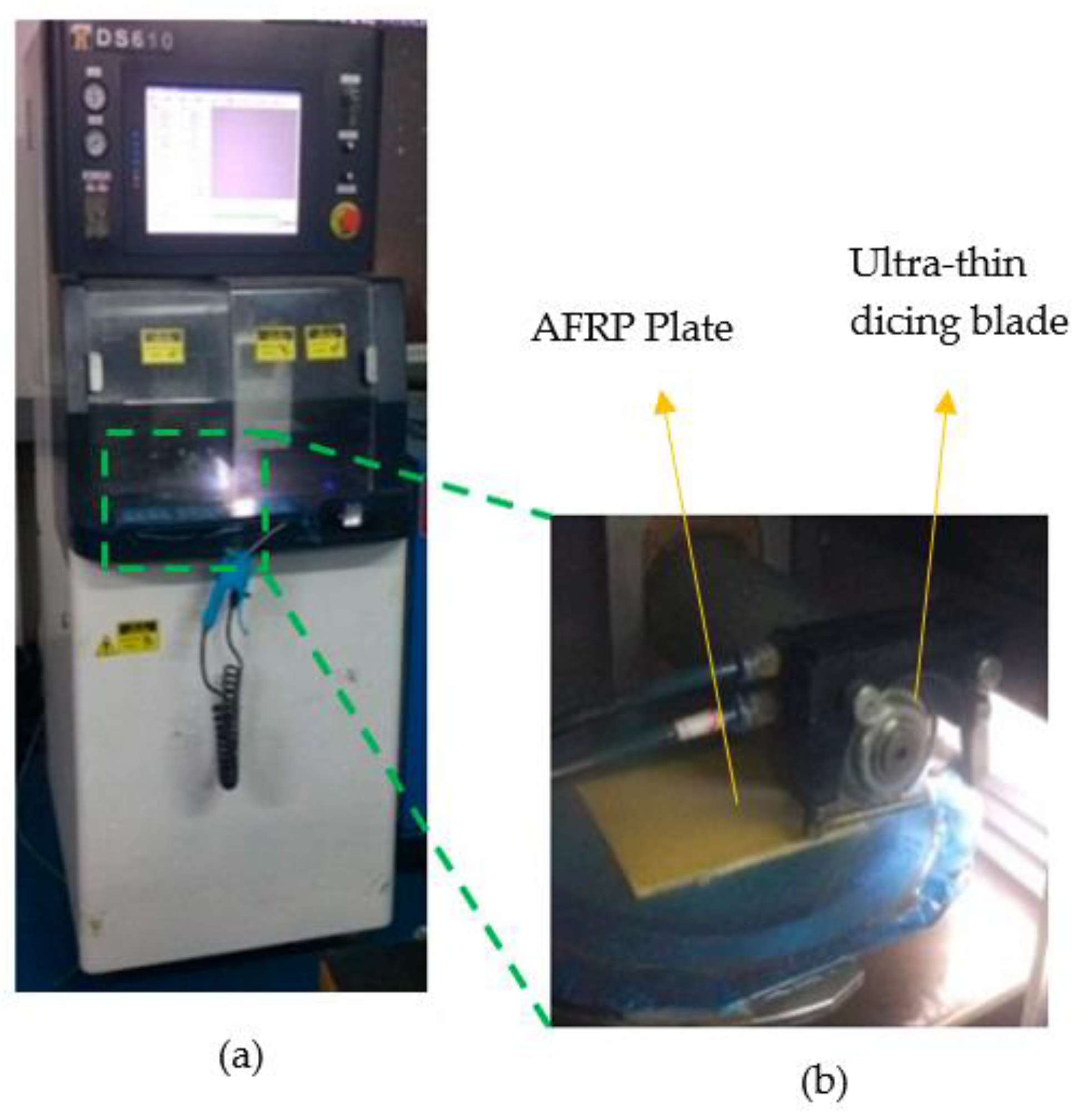
  52. Wen, Q.; Hu, J.; Yuan, Z. Sub-Fiber Scale Precision Dicing of Aramid Fiber-Reinforced Plastic Composites. Mac 2022, 10, 334. [Google Scholar] [CrossRef]
  53. Kim, S.-C.; Lee, E.-S.; Kim, N.-H.; Jeong, H.-D. Machining characteristics on the ultra-precision dicing of silicon wafer. Int. J. Adv. Manuf. Technol. 2007, 33, 662–667. [Google Scholar] [CrossRef]
  54. Wang, X.; Yuan, Z.; Zhuang, P.; Wu, T.; Feng, S. Study on precision dicing process of SiC wafer with diamond dicing blades. Nanotech. Prec. Eng. 2021, 4, 033004. [Google Scholar] [CrossRef]
  55. Ma, Y.; Jiang, X.; Cao, Z.; Liu, H.; Li, D. Simulation and Analysis on the Influence of Diamond Blade Cutting Parameters of Grinding Wheel Dicing Saw. In Journal of Physics: Conference Series; IOP Publishing Ltd.: Shenzhen, China, 2022. [Google Scholar]
  56. Inoue, F.; Podpod, A.; Peng, L.; Phommahaxay, A.; Rebibis, K.J.; Uedono, A.; Beyne, E. Morphological characterization and mechanical behavior by dicing and thinning on direct bonded Si wafer. J. Manuf. Proc. 2020, 58, 811–818. [Google Scholar] [CrossRef]
  57. Steiert, M.; Wilde, J. Influence of dicing damages on the thermo-mechanical reliability of bare-chip assemblies. MiRe 2014, 54, 1686–1691. [Google Scholar] [CrossRef]
  58. Bifano, T.G.; Dow, T.A.; Scattergood, R.O. Ductile-regime grinding: A new technology for machining brittle materials. J. Manuf. Sci. Technol. 1991, 113, 184–189. [Google Scholar] [CrossRef]
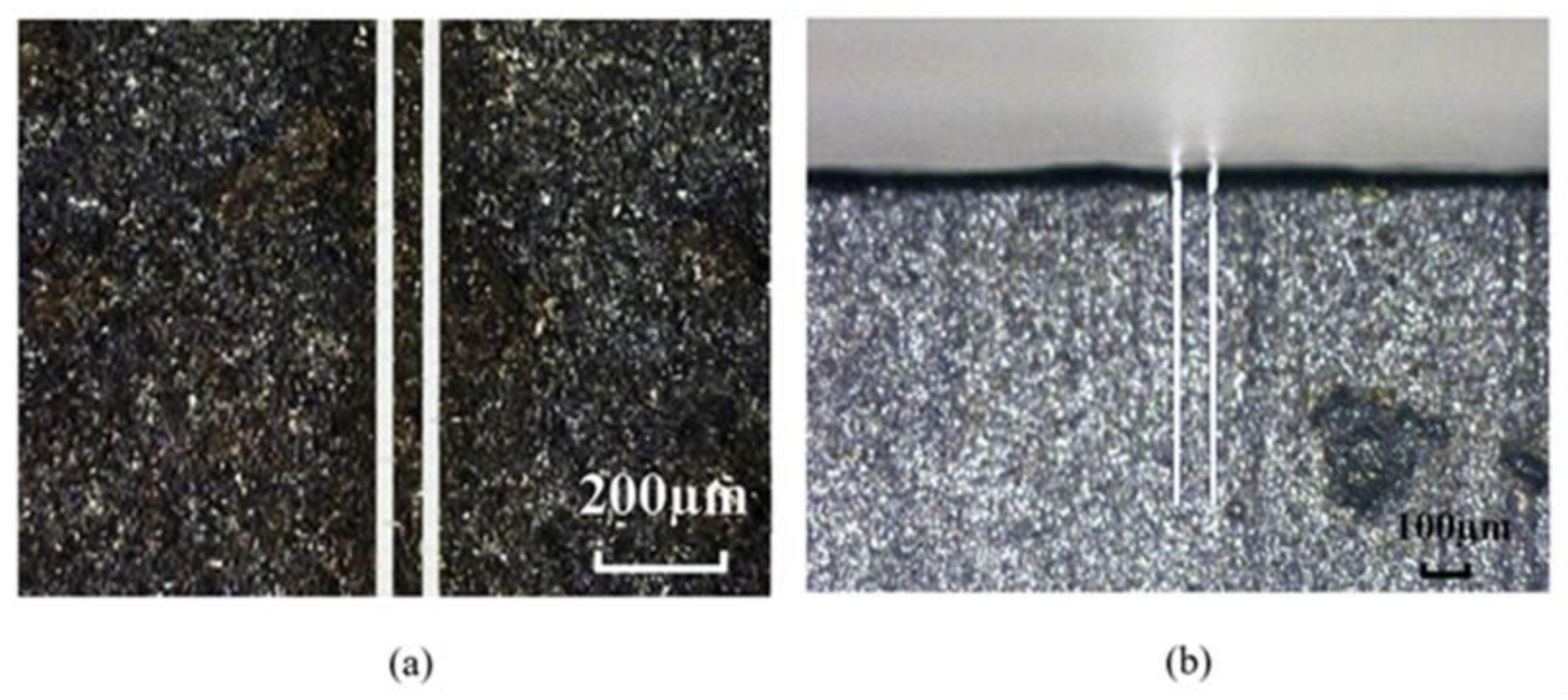
  59. Luo, S.; Wang, Z. Studies of chipping mechanisms for dicing silicon wafers. Int. J. Adv. Manuf. Technol. 2008, 35, 1206–1218. [Google Scholar] [CrossRef]
  60. Mulembo, T.; Ikua, B.; Keraita, J.; Niyibizi, A.; Wangui, E. Developments in Silicon Wafer Micromachining. In Proceedings of the Sustainable Research and Innovation Conference, Juji, Kenya, 3–4 May 2012. [Google Scholar]
  61. Yang, L. Prediction of steady-state wear coefficients in adhesive wear. Trib.Trans. 2004, 47, 335–340. [Google Scholar] [CrossRef]
  62. Lin, J.-W.; Cheng, M.-H. Investigation of chipping and wear of silicon wafer dicing. J. Manuf. Proc. 2014, 16, 373–378. [Google Scholar] [CrossRef]
  63. Yang, L. A test methodology for the determination of wear coefficient. Wear 2005, 259, 1453–1461. [Google Scholar] [CrossRef]
  64. Zhou, H.; Qiu, S.; Huo, Y.; Zhang, N. High-speed dicing of silicon wafers conducted using ultrathin blades. Int. J. Adv. Manuf. Technol. 2013, 66, 947–953. [Google Scholar] [CrossRef]
  65. Fuegl, M.; Mackh, G.; Meissner, E.; Frey, L. Analytical stress characterization after different chip separation methods. MiRe 2014, 54, 1735–1740. [Google Scholar] [CrossRef]
  66. Liu, S.Q.; Chen, Y.; Fu, Y.C.; Hu, A.D. Study on the cutting force and machined surface quality of milling AFRP. MSF 2016, 836, 155–160. [Google Scholar] [CrossRef]
  67. El-Taweel, T.; Abdel-Maaboud, A.; Azzam, B.; Mohammad, A. Parametric studies on the CO2 laser cutting of Kevlar-49 composite. Int. J. Adv. Manuf. Technol. 2009, 40, 907–917. [Google Scholar] [CrossRef]
  68. Xu, W.; Zhang, L. On the mechanics and material removal mechanisms of vibration-assisted cutting of unidirectional fibre-reinforced polymer composites. Int. J. Mach. Tol. Manuf. 2014, 80, 1–10. [Google Scholar] [CrossRef]
  69. Thakur, R.; Singh, K. Abrasive waterjet machining of fiber-reinforced composites: A state-of-the-art review. J. Br. Sc. Mech. Sci. Eng. 2020, 42, 1–25. [Google Scholar] [CrossRef]
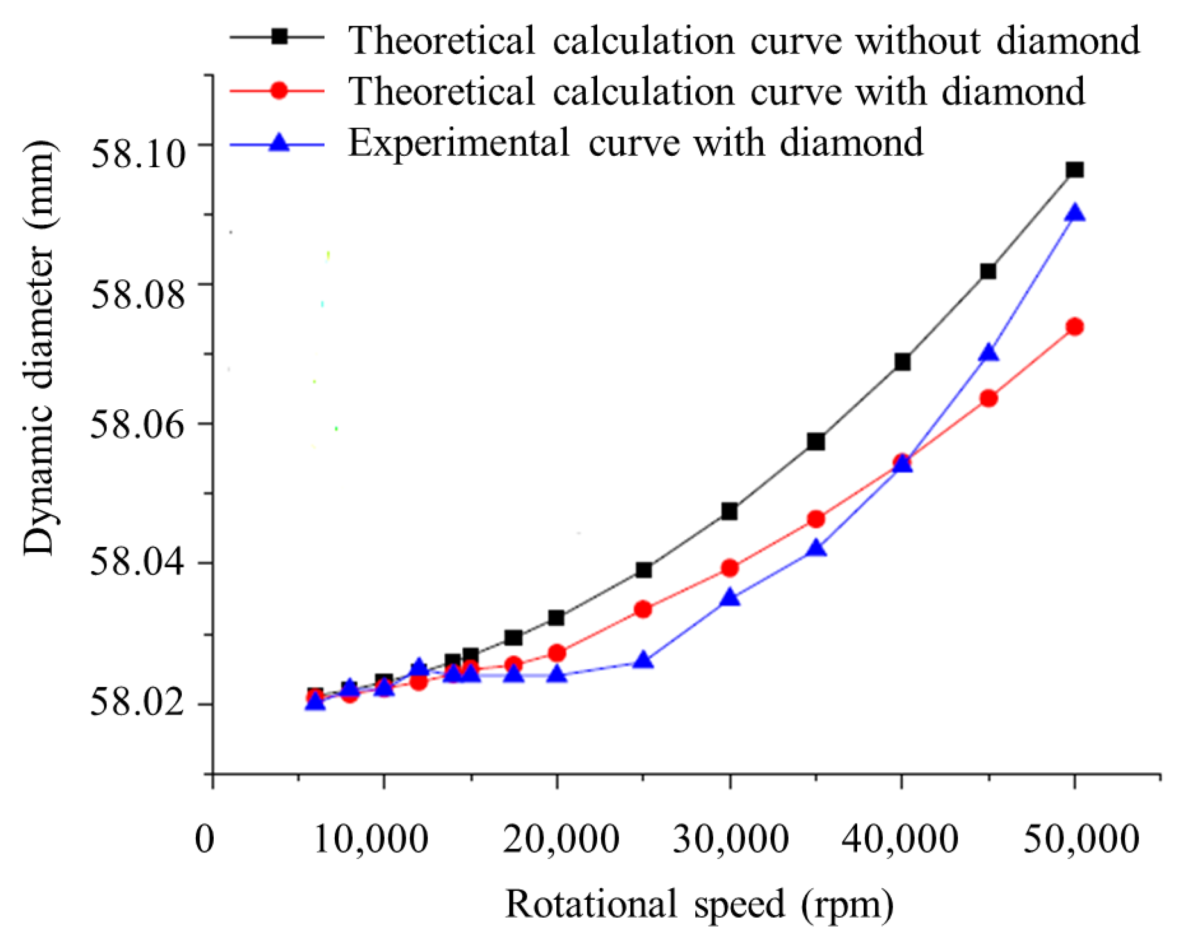
  70. Li, K.; Wang, M.; Chen, F.; Yan, N.; Zou, Q.; Zhao, Y.; Li, J.; Zhao, F. Analysis of the Dynamic Diameter of Superthin Diamond Blades in the High Speed and Precison Dicing Process. Int. J. Prec. Eng. Manuf. 2019, 20, 1071–1081. [Google Scholar] [CrossRef]
  71. Li, K.; Wang, Y.; Zhao, Y.; Jin, C.; Tang, H.; Zou, Q.; Zhao, Y.; Wang, M. High strain rate of quartz glass and its effects during high-speed dicing. Ceram. Int. 2019, 45, 13523–13529. [Google Scholar] [CrossRef]
  72. Matsumaru, K.; Takata, A.; Ishizaki, K. Advanced thin dicing blade for sapphire substrate. Sci. Technol. Adv. Mat. 2005, 6, 120–122. [Google Scholar] [CrossRef]
  73. Touge, M.; Watanabe, J.; Matsuo, T. Ultra-thinning processing of dielectric substrates by precision abrasive machining. CIRP Ann. 2006, 55, 317–320. [Google Scholar] [CrossRef]
  74. Carpenter, L.; Holmes, C.; Cooper, P.; Gates, J.; Smith, P. Precision dicing of optical materials. In Proceedings of the SPIE—The International Society for Optical Engineering, San Francisco, CA, USA, 3–5 February 2014. [Google Scholar]
  75. Carpenter, L.; Rogers, H.; Holmes, C.; Gates, J.; Smith, P. Polish-like facet preparation via dicing for silica integrated optics. In Proceedings of the SPIE—The International Society for Optical Engineering, San Francisco, CA, USA, March 2013. [Google Scholar]
  76. Chen, S.; Tsai, C.; Wu, E.; Shih, I.; Chen, Y. Study on the effects of wafer thinning and dicing on chip strength. IEEE Trans. Adv. Packg. 2006, 29, 149–157. [Google Scholar] [CrossRef]
  77. Stompe, M.; Cvetkovic, S.; Rissing, L. Blade wear and sidewall quality by dicing of sintered silicon carbide (SSiC). In Proceedings of the 11th Euspen International Conference, Como, Italy, 23–26 May 2011. [Google Scholar]
  78. Wang, P.; Li, M.; Gao, L.; Meng, H.; Mu, D. The Evaluation of CHIPPING on Single-Crystal Silicon Carbide (SiC) Dicing Machining Using Sintered Diamond Blades. Available online: https://www.spiedigitallibrary.org/conference-proceedings-of-spie/12244/122440F/The-evaluation-of-chipping-on-single-crystal-silicon-carbide-SiC/10.1117/12.2634895.short (accessed on 20 January 2023).
  79. Lim, S.; Zamri, M.; Yusoff, A. Structure Integrity Analysis on Nickel–Diamond Blade in Dicing of Hard-brittle Ceramic Die. Procedia CIRP 2022, 108, 465–469. [Google Scholar] [CrossRef]
  80. Semiconductor Manufacturing Process (Back-End Process). Available online: https://www.matsusada.com (accessed on 14 November 2022).
  81. Integrated Circuit Manufacturing and Chipping Damage. Available online: https://www.olympus-ims.com (accessed on 14 November 2022).
  82. Wang, C.; Zhang, M.; Chen, X.; Bertrand, M.; Shams-Ansari, A.; Chandrasekhar, S.; Winzer, P.; Loncar, M. Integrated lithium niobate electro-optic modulators operating at CMOS-compatible voltages. Nature 2018, 562, 101–104. [Google Scholar] [CrossRef] [PubMed]
  83. Wang, S.; Zhao, J.; Gu, J.; Bu, M.; Fan, L.; Li, S.; Qin, X.; Yao, Y.; Ren, Y.; Wang, L. Study on LiNbO3 Channel and Ridge Waveguides-Based on Helium Ion Implantation Combined with Lithography and Precise Diamond Dicing. Available online: https://www.researching.cn/HiringPubPDF/COL-22-0074.pdf (accessed on 20 January 2023).
  84. Ríos, C.; Stegmaier, M.; Hosseini, P.; Wang, D.; Scherer, T.; Wright, C.D.; Bhaskaran, H.; Pernice, W.H. Integrated all-photonic non-volatile multi-level memory. Nat. Photon. 2015, 9, 725–732. [Google Scholar] [CrossRef]
  85. Jia, Y.; Rüter, C.E.; Akhmadaliev, S.; Zhou, S.; Chen, F.; Kip, D. Ridge waveguide lasers in Nd: YAG crystals produced by combining swift heavy ion irradiation and precise diamond blade dicing. Opt. Mat. Exp. 2013, 3, 433–438. [Google Scholar] [CrossRef]
  86. Liu, C.-X.; You, J.-L.; Lin, S.-Q.; Chen, J.-Y.; Tang, M.; Lin, S.-B.; Zheng, R.-L.; Fu, L.-L.; Zhang, L.-L. A ridge waveguide constructed by H+ implantation and precise diamond blade dicing in high-gain Nd3+-doped laser glass. Optik 2021, 225, 165881. [Google Scholar] [CrossRef]
  87. Yashar, A.B.; Ilan, H.; Agranat, A.J. Construction of waveguiding structures in potassium lithium tantalate niobate crystals by combined laser ablation and ion implantation. Appl. Phys. A 2015, 118, 403–407. [Google Scholar] [CrossRef]
  88. Zhao, J.; Ye, L.; Liu, Y.; Li, S.; Fu, G.; Yue, Q. Optical properties and surface blistering visualization on multiple-energy He-implanted Yb: YGG crystal by annealing treatment. Results Phys. 2019, 15, 102621. [Google Scholar] [CrossRef]
  89. Bentini, G.; Bianconi, M.; Chiarini, M.; Correra, L.; Sada, C.; Mazzoldi, P.; Argiolas, N.; Bazzan, M.; Guzzi, R. Effect of low dose high energy O3+ implantation on refractive index and linear electro-optic properties in X-cut LiNbO3: Planar optical waveguide formation and characterization. J. Appl. Phys. 2002, 92, 6477–6483. [Google Scholar] [CrossRef]
  90. Chen, F.; Tan, Y.; Jaque, D. Ion-implanted optical channel waveguides in neodymium-doped yttrium aluminum garnet transparent ceramics for integrated laser generation. Opt. Lett. 2009, 34, 28–30. [Google Scholar] [CrossRef] [PubMed]
  91. García-Navarro, A.; Olivares, J.; García, G.; Agulló-López, F.; García-Blanco, S.; Merchant, C.; Aitchison, J.S. Fabrication of optical waveguides in KGW by swift heavy ion beam irradiation. Nucl. Instrum. Methods Phys. Res. B 2006, 249, 177–180. [Google Scholar]
  92. Montanari, G.; De Nicola, P.; Sugliani, S.; Menin, A.; Parini, A.; Nubile, A.; Bellanca, G.; Chiarini, M.; Bianconi, M.; Bentini, G. Step-index optical waveguide produced by multi-step ion implantation in LiNbO3. Opt. Express 2012, 20, 4444–4453. [Google Scholar] [CrossRef]
  93. Ren, Y.; Dong, N.; Chen, F.; Jaque, D. Swift nitrogen ion irradiated waveguide lasers in Nd: YAG crystal. Opt. Express 2011, 19, 5522–5527. [Google Scholar] [CrossRef]
  94. Gattass, R.R.; Mazur, E. Femtosecond laser micromachining in transparent materials. Nat. Photon. 2008, 2, 219–225. [Google Scholar] [CrossRef]
  95. Zolotoyabko, E.; Avrahami, Y.; Sauer, W.; Metzger, T.; Peisl, J. High-temperature phase transformation in Ti-diffused waveguide layers of LiNbO3. Appl. Phys. Lett. 1998, 73, 1352–1354. [Google Scholar] [CrossRef]
  96. Liu, T.; Kong, W.; Liu, C. Surface behavior in potassium titanyl phosphate crystal irradiated by swift Kr8+ ions. Opt. Express 2019, 58, 096110. [Google Scholar] [CrossRef]
  97. Tan, Y.; Chen, F.; Wang, L.; Wang, K.-M.; Lu, Q.-M. Thermal stability of carbon-ion-implanted Nd: YVO4 optical planar waveguide. JKPS 2008, 52, 80. [Google Scholar] [CrossRef]
  98. Wang, Y.; Zhao, J.; Zhu, Q.; Shen, J.; Wang, Z.; Guo, H.-T.; Liu, C. Near-infrared carbon-implanted waveguides in Tb3+-doped aluminum borosilicate glasses. Front. Optoelec. 2019, 12, 392–396. [Google Scholar] [CrossRef]
  99. Zhou, Y.-F.; Wang, L.; Liu, P.; Liu, T.; Zhang, L.; Huang, D.-T.; Wang, X.-L. Ridge waveguide fabrication by combining ion implantation and precise dicing on a LiNbO3 crystal. Nucl. Instrum. Methods Phys. Res. B 2014, 326, 110–112. [Google Scholar]
  100. Cheng, Y.; Lv, J.; Akhmadaliev, S.; Zhou, S.; Kong, Y.; Chen, F. Mid-infrared ridge waveguide in MgO: LiNbO3 crystal produced by combination of swift O5+ ion irradiation and precise diamond blade dicing. Opt. Mater. 2015, 48, 209–214. [Google Scholar] [CrossRef]
  101. Cheng, Y.; Lv, J.; Chen, F. Mid-infrared ZnSe ridge waveguides fabricated by swift Kr8+ ion irradiation combined with precise diamond blade dicing. Opt. Mat. Exp. 2015, 5, 2292–2299. [Google Scholar] [CrossRef]
  102. Luan, Q.; Tan, Y.; Akhmadaliev, S.; Zhou, S.; Yu, H.; Zhang, H.; Chen, F. Optical ridge waveguides in Nd: CNGG disorder laser crystal produced by combination of carbon ion irradiation and precise diamond blade dicing. Opt. Mater. 2015, 39, 247–250. [Google Scholar] [CrossRef]
  103. Chen, C.; Luan, Q.; He, R.; Cheng, C.; Akhmadaliev, S.; Zhou, S.; Yu, H.; Zhang, H.; Chen, F. Ridge waveguides in Nd: ABC3O7 disordered crystals produced by swift C5+ ion irradiation and precise diamond dicing: Broad band guidance and spectroscopic properties. Opt. Laser Technol. 2015, 68, 84–88. [Google Scholar] [CrossRef]
  104. Cheng, Y.; Lv, J.; Akhmadaliev, S.; Zhou, S.; Chen, F. Optical ridge waveguides in Nd: LGS crystal produced by combination of swift C5+ ion irradiation and precise diamond blade dicing. Opt. Laser Technol. 2016, 81, 122–126. [Google Scholar] [CrossRef]
  105. Li, R.; Nie, W.; Shang, Z.; Cheng, C.; Akhmadaliev, S.; Zhou, S.; Lu, Q.; Chen, F. Guided-wave second harmonics in Nd:YCOB ridge waveguides produced by combination of carbon ion irradiation and precise diamond blade dicing. Opt. Mater. 2016, 57, 153–157. [Google Scholar] [CrossRef]
  106. Xu, H.; Li, Z.; Pang, C.; Li, R.; Li, G.; Akhmadaliev, S.; Zhou, S.; Lu, Q.; Jia, Y.; Chen, F. Second harmonic generation from precise diamond blade diced ridge waveguides. Chin. Phys. B 2022, 31, 094209. [Google Scholar] [CrossRef]
  107. Chen, C.; Lu, Q.; Akhmadaliev, S.; Zhou, S. Diamond-blade diced trapezoidal ridge waveguides in YCOB crystal for second harmonic generation. Opt. Laser Technol. 2020, 126, 106128. [Google Scholar] [CrossRef]
  108. Cheng, Y.; Song, H.; Li, S. Infrared LiF ridge waveguide fabricated by carbon ion irradiation. Laser Phys. 2022, 32, 126201. [Google Scholar] [CrossRef]
  109. Volk, M.F.; Rüter, C.E.; Santandrea, M.; Eigner, C.; Padberg, L.; Herrmann, H.; Silberhorn, C.; Kip, D. Fabrication of low-loss Rb-exchanged ridge waveguides in z-cut KTiOPO4. Opt. Mat. Exp. 2018, 8, 82–87. [Google Scholar] [CrossRef]
  110. Zhang, J.; Guo, W.-T.; Tang, C.-Y.; Yan, S.; Li, W.-N.; Liu, C.-X. Planar and ridge waveguides in Yb3+-doped silicate glasses fabricated by proton implantation and precise diamond blade dicing. Opt. Commun. 2019, 453, 124344. [Google Scholar] [CrossRef]
  111. Loiko, P.; Gauthier-Manuel, L.; Brasse, G.; Kifle, E.; Guillemot, L.; Braud, A.; Benayad, A.; Menard, V.; Camy, P. Channel waveguide lasers in bulk Tm: LiYF4 produced by deep diamond-saw dicing. Opt. Express 2020, 28, 26676–26689. [Google Scholar] [CrossRef]
  112. Loiko, P.; Gauthier-Manuel, L.; Brasse, G.; Braud, A.; Benayad, A.; Camy, P. Efficient wavelength-tunable deep-diced ridge waveguide lasers in bulk Yb3+: CaF2 crystal. Opt. Mater. 2021, 113, 110861. [Google Scholar] [CrossRef]
  113. Grootes, R.; Dijkstra, M.; Klaver, Y.; Marpaung, D.; Offerhaus, H. Crack barriers for thick SiN using dicing. Opt. Express 2022, 30, 16725–16733. [Google Scholar] [CrossRef]
  114. Cvetković, S.; Morsbach, C.; Rissing, L. Ultra-precision dicing and wire sawing of silicon carbide (SiC). Microelectron. Eng. 2011, 88, 2500–2504. [Google Scholar] [CrossRef]
Figure 1. Die separation techniques: (a) diamond scribing; (b) laser scribing; (c) diamond wheel dicing; (d) ultrasonic dicing; (e) stealth dicing; (f) plasma dicing [7,9,11,12]. Adapted with permission from Ref. [11]. 2015, Elsevier.
Machines 11 00259 g001
Figure 2. Search process and results, adapted from PRISMA [14].
Machines 11 00259 g002
Figure 3. Preparation of dicing blades [15].
Machines 11 00259 g003
Figure 4. (a) Elements of the abrasive product in dicing blade; SEM micrograph of dicing blade fabricated from (b) SPS; (c) vacuum sintering [13,16].
Machines 11 00259 g004
Figure 5. Groove cut with thin PCD blade before and after trusion [27].
Machines 11 00259 g005
Figure 6. Principle of continuous laser dressing. Adapted with permission from Ref. [30]. 2013, Elsevier.
Machines 11 00259 g006
Figure 7. (a) Signal analysis of five cuts before laser dressing; (b) signal analysis of five cuts after laser dressing [32].
Machines 11 00259 g007
Figure 8. Fine grooving of cemented carbide (groove depth 1 mm, width 20 μm, and length 8 mm): (a) top view of deep grooves; (b) cross-sectional view of deep grooves. Adapted with permission from Ref. [39]. 2018, Elsevier.
Machines 11 00259 g008
Figure 9. (a) Concept of dual dicing; silicon dicing results comparing single and dual dicing for (b) chipping (c) sidewall angles [41].
Machines 11 00259 g009
Figure 10. (a) Chip measuring procedure [45]; (b) top view of the chipping for directly bonded wafer after dicing; defects due to the blade dicing. Adapted with permission from Ref. [56]. 2020, Elsevier; (c) chipping at the front side edge; (d) cracks at the side wall; (e) chipping at the back side edge. Adapted with permission from Ref. [57]. 2014, Elsevier.
Machines 11 00259 g010
Figure 11. Distribution of abrasive particles on dicing blade surface: (a) sparse; (b) dense [52].
Machines 11 00259 g011
Figure 12. Surface morphology of AFRP composites after dicing: (a) morphology of the groove side; (b) schematic diagram of dicing mechanism with different fiber orientations for CFRP composites; (c) dicing direction parallel to fiber orientation; (d) dicing direction perpendicular to fiber orientation; (e) dicing direction with an angle of 45° to fiber orientation; (f) dicing direction with an angle of 135° to fiber orientation [48,52].
Machines 11 00259 g012
Figure 13. Variation of blade surface roughness vs. cutting distance. Adapted with permission from Ref. [62]. 2014, Elsevier.
Machines 11 00259 g013
Figure 14. Surface morphologies of diced CFRP composites for metal-bonded blades at fiber orientations (a) 0°; (b) 40°; (c) 90°; and (d) 130° and for resin-bonded blades at fiber orientations (e) 0°; (f) 40°; (g) 90°; and (h) 130° [48].
Machines 11 00259 g014
Figure 15. Dicing AFRP composite fiber with dicing machine [52]. (a) Dicing machine; (b) tool and workpiece material.
Machines 11 00259 g015
Figure 16. Dynamic diameter variations at different rotational speeds. Adapted with permission from Ref. [70]. 2018, Elsevier.
Machines 11 00259 g016
Figure 17. (a) Sapphire surface, after cutting by a commercial dicing blade, generates meandering lines and breaks after 50 mm of cutting length; (b) sapphire surface after cutting by fabricated dicing, where all blades can cut 1000 mm [72].
Machines 11 00259 g017
Figure 18. (a) A dicing machine (Loadpoint, MicroAce, Series 3) with the axes of movement and the coolant supply; microscopic image for ductile machining of (b) germanium; (c) YAG; (d) lithium niobate; (e) silicon [74].
Machines 11 00259 g018
Figure 19. (a) Average wearing on the blades as a function of the feed speed for the rotations of 10,000, 20,000, and 30,000 rpm; (b) chip strength of a wafer diced at feeding rates of 100, 75, and 50 mm/s [45,76].
Machines 11 00259 g019
Figure 20. Back-end process: (a) dicing; (b) die bonding; and (c) molding [80,81].
Machines 11 00259 g020
Figure 21. Schematics of (a) 3 MeV oxygen ion implantation; (b) diamond blade dicing; (c) cross-sections of the ridge waveguides; (d) transmission optical microscopy image showing a close-up of the ridge waveguide [99].Adapted with permission from Ref. [99]. 2014, Elsevier.
Machines 11 00259 g021
Figure 22. Scheme of the deep diced ridge WGs in bulk Tm3+: LiYF4 crystal (the end-facet view) [111].
Machines 11 00259 g022
Figure 23. Comparison of machining techniques for (a) monocrystalline and (b) ceramic substrates; SEM micrographs of edges after dicing of (c) monocrystalline and (d) ceramic substrates; for alumina, (e) channels generated after the surface grinding; (f) profile of the cross-section roughness; (g) channel generated on the surface after the dicing process; (h) profile of roughness measured on the channel [45,114]. Adapted with permission from Ref. [114]. 2011, Elsevier.
Machines 11 00259 g023
Figure 24. White light interferometer images for (a) germanium; (b) YAG; (c) lithium niobate; (d) silicon [74].
Machines 11 00259 g024
Table 1. Components of three dicing blades [15].
Matrix Composition (Mass Ratios %)
1.CuSn33 (32) + CuZn20 (18) + Co (20) + YA520 (30)
2.CuSn40 (25) + Cu (50) + Sn (5) + CuSn10 (20)
3.Cu (70) + Sn (18) + Zn (5) + Ni (7)
Disclaimer/Publisher’s Note: The statements, opinions and data contained in all publications are solely those of the individual author(s) and contributor(s) and not of MDPI and/or the editor(s). MDPI and/or the editor(s) disclaim responsibility for any injury to people or property resulting from any ideas, methods, instructions or products referred to in the content.

