Review

Topological Overview of Auxiliary Source Circuits for Grid-Tied Converters †

1
Department of Electrical and Electronics Engineering, Faculty of Engineering, Ariel University, Ariel 4070000, Israel
2
School of Electrical and Computer Engineering, Ben Gurion University, Beer-Sheva 8410501, Israel
*
Author to whom correspondence should be addressed.
This paper is an extended version of a conference paper ‘Synopsis on Electronic Capacitor for Grid-Tied Converters’ published in 2022 IEEE 23rd Workshop on Control and Modeling for Power Electronics (COMPEL).
Machines 2023, 11(2), 171; https://doi.org/10.3390/machines11020171
Submission received: 30 November 2022 / Revised: 23 January 2023 / Accepted: 23 January 2023 / Published: 27 January 2023
(This article belongs to the Special Issue Advances in High-Power Converters)

Abstract

:
This paper reviews different types of capacitors and auxiliary source circuit topologies and presents an introduction to control strategies used for circuit applications reducing DC-BUS capacitance. The paper argues in favor of replacing bulky electrolytic capacitors in capacitor-supported power electronic systems with auxiliary source circuits. DC-BUS capacitors are widely used in grid-tied power converters (rectifiers) and utilized for power balance, voltage ripple limitation, and short-term energy storage. The electrolyte capacitor is the Achilles heel of any rectifier and power converter due to its higher rate of failure than other circuitry components. Auxiliary source circuits are key components to qualitatively improve the reliability of the DC links, where they divert the instantaneous pulsating power into extra reliable storage components. Unlike previous work, this review serves to provide a clear picture of an auxiliary source circuit design, in favor of optimal solution selection according to the specific application. Therefore, energy storage components (capacitors), topologies, and control strategies of auxiliary source circuits are comprehensively reviewed in this paper. Additionally, detailed explanations, comparisons, and discussions of auxiliary source circuits are offered.

1. Introduction

Grid-tied power converters produce a predetermined current shape that fulfills standardization requirements for appropriate power quality [1,2]. As a result, the rectified output voltage is forced to contain two different current components: dynamic and static. Moreover, loads that are connected through the interfacing converter can also consume two similar power components: average and pulsating. Because the loads on average consume constant power, while the grid supplies pulsating power, a buffer is required to stabilize the power equation.
In general, a common energy conversion from the grid to the load is performed by two-stage converters: a first-stage interface converter (FSIC) and a second-stage interface converter (SSIC). A bulky capacitor is employed as the buffer to ensure the equality of input/output power balancing. Furthermore, in [3,4], it was shown that capacitive impedance is advantageous in terms of power quality and grid stability. Therefore, adding a bulky electrolytic capacitor to the DC-BUS terminals is the commonly implemented solution [5]. The use of capacitors/passive elements is inevitable in power rectification systems to maintain proper functionality. Figure 1 shows the presently common topology for a generalized two-stage, grid-connected power conversion system, with a bulky electrolyte capacitor (BEC) on the DC-BUS terminals. I’ and V’ represent the current and voltage of the SSIC, respectively. The energy flow direction across the SSIC is bidirectional, for example, in cases when a typical load or a solar panel is connected to the power grid.
The compulsory power quality requirement from grid-tied rectifiers creates a low-frequency voltage ripple (VR) at the DC-BUS capacitors. The undesirable VR leads to inferior converter performance [6] by increasing voltage fluctuations, reducing the harvesting efficiency of the photovoltaic (PV) panels [7], intensifying LED flicker (lighting applications) [8,9,10], overheating and reducing the batteries’ lifespan [11,12], and, most importantly, by shortening the electrolytic capacitor’s lifetime. The major advantage of an electrolytic capacitor over other types, such as film, ceramic, and tantalum, is their higher volumetric energy density. It is often the preferred choice in power electronics applications, where high capacitance and compactness are important [13].
Unfortunately, the BECs usually comprise the system’s drawbacks in terms of reliability, lifetime, weight, and size [14]. Therefore, it is imperative to preserve the VR within the predetermined limits to avoid damaging the DC-BUS capacitors or exceeding the SSIC input limits. The VRs are correlated with the power conversion system rating and uncorrelated with the DC-BUS capacitance; by increasing the capacitor value, the VR can be reduced. The multiplicity faults in the BEC occur for two main reasons: (a) voltage fluctuation sensitivity, with emphasis on peak voltage (forced to use 90% of the maximum voltage value) and (b) temperature rise sensitivity (e.g., a drop of 10 degrees doubles the capacitor’s lifespan). In addition, due to the capacitor temperature rise, numerous faults are created in other electronic components in its environment, hence the need to implement a suitable replacement for BECs in power converters.
Most of the methods currently used as a suitable replacement for BECs are based on adding an auxiliary source circuit (ASC) that imitates the dynamic capacitor behavior [15]. A virtual capacitor with an infinite capacitance range (as far as possible) can be obtained by replacing the electrolyte capacitor with an ASC unit based on an appropriate control strategy (Section 3). The ASC is based on a bidirectional DC/DC converter [16] and auxiliary capacitor “ C A ” (nonelectrolyte technology) with a small capacitance value (smaller by several orders of magnitude than an electrolyte capacitor). The currently common topologies for integrating an ASC unit with a generalized two-stage, grid-tied power conversion system is a series connection with the converter/capacitor side and shunt connection, as presented in Figure 2. The main gap between the topologies is the absence of a DC-BUS capacitor “C” in the shunt connection; this approach allows to replace the DC-BUS capacitor with an ASC (extended explanation in Section 3).
Despite the electrolyte capacitor benefits mentioned above, the equivalent series resistance (ESR) of a film capacitor is invariably lower than the ESR of an electrolytic one across the entire frequency range. In addition, the ESR value of the electrolyte capacitor is significantly decreased as the temperature rises (much more than that of the film capacitor). Moreover, the evaluation confirms that film capacitor utilization yields benefits in terms of improved power density, reduced power losses, low parasitic inductance, and extended lifetime compared to an electrolyte capacitor [17,18,19]. As a result, the most popular capacitor technology for the auxiliary capacitor implemented in an ASC is a small film capacitor [20]. Therefore, to achieve optimal design (high reliability, reduced temperature sensitivity, longer lifespan, and smaller physical size) for power conversion systems, the electrolyte capacitor can be replaced with an ASC unit (based on a film capacitor with a much lower capacitance value compared to the electrolyte). Hence, the ASC unit allows limiting the steady-state DC-BUS VRs while reducing the utilized capacitance [21].
In this paper, a comprehensive review of ASC-typical capacitors, topologies, and control strategies is presented. The literature presents several solutions to these challenges, and some review reports have been made as mentioned in the introduction. Nonetheless, to achieve a wide range of optimal solutions, it is necessary to introduce a clear picture for all questions in the ASC design process. The ASC design process includes three main considerations: the selection of an energy storage source, topology, and control strategy. The effort to overcome the above challenges is divided into three steps: (a) selecting an optimal DC-BUS capacitor (according to source/load conditions); (b) choosing a suitable topology for implementing an ASC in a power conversion system; and (c) determining an appropriate smart control technique for implementing the strategy according to the system requirements. Therefore, this paper presents a comprehensive overview focused on the following subjects: Section 1 introduces the problems and challenges of a power conversion system based on an electrolytic capacitor. Next, Section 2 presents an extensive overview and discussion on typical capacitors (electrolytic, ceramic, and film) for applications in power conversion systems (with performance comparison). In Section 3, common control strategies for reducing DC-BUS capacitance in circuit applications are classified, presenting control techniques and detailing advantages/disadvantages accordingly. Then, in Section 4, the available ASCs are investigated with a detailed analysis and comparison; in addition, the alternative approaches are further discussed and evaluated to select the most suitable topologies for future capacitor-supported power conversion systems. Some conclusions are drawn in Section 5.

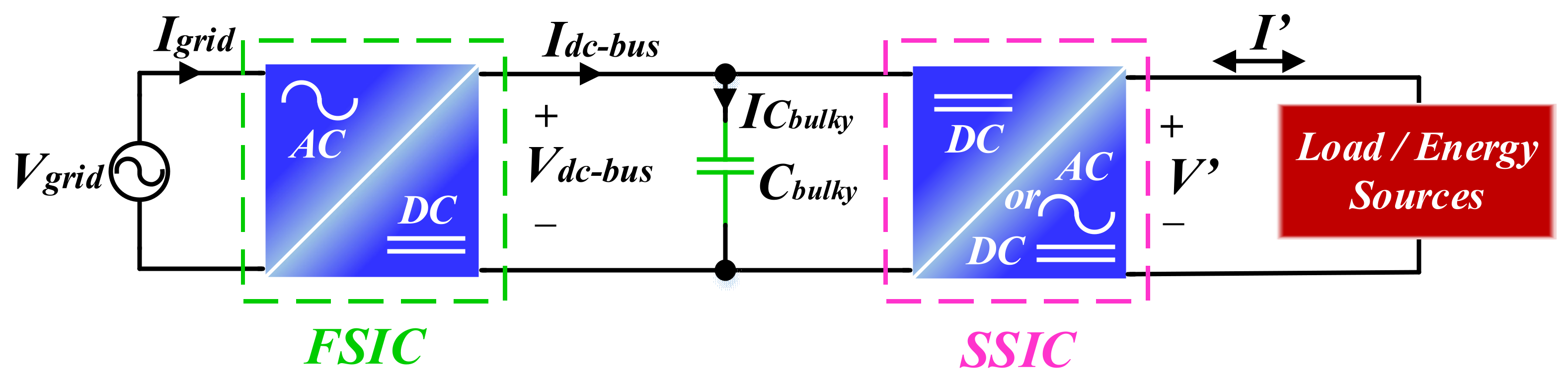
2. DC-BUS Capacitors

2.1. Common Types of DC-BUS Capacitors

A major requirement of the power converter is to employ capacitors on DC-BUS terminals for a variety of reasons, such as input/output power balancing, harmonics absorption, short-term period energy storage, and suppressing the VR [22,23,24,25]. Capacitor utilization is most common in power conversion systems, such as off-line converters, lighting drivers, full/hybrid electric propulsion systems [26], and a variety of renewable-energy applications [27]. The BEC is employed in a parallel connection to the DC-BUS terminals, as can be seen in Figure 1. When diagnosing the power converter’s reliability, doubtlessly the weakest link in the conversion system is the electrolyte capacitor, due to its short lifespan and high degradation failure rate [28,29]. A detailed analysis of power converters under DC-BUS capacitor failure and a presentation of their effect on inverter electrical characteristics was previously performed in [30]. Moreover, about 30% of power converter failures are caused by the deterioration of the capacitors [31], as can be seen in the failure distribution chart among major components shown in Figure 3a. However, the capacitor’s environmental conditions can also intensify the degradation and increase the failure rate, as presented in the distribution chart of stress sources leading to failures in Figure 3b. Therefore, due to the high failure rate, power converter size limitations, and the surrounding environmental conditions (e.g., high humidity, high ambient temperature, etc.), an optimal DC-BUS capacitor selection should be performed for power conversion systems [32].
An optimum DC-BUS capacitor selection means choosing such capacitors for power converters that provide a satisfactory solution to a variety of requirements, such as high reliability, lowest possible volume and/or weight, and minimal cost. Consequently, there is great importance placed on a preliminary analysis of the capacitor characteristics for optimal DC-BUS capacitor selection. The three most common types of capacitors for power converter applications discussed in this article are Aluminum Electrolytic Capacitors (AE-Cs), high-capacitance Multilayer Ceramic Capacitors (MLC-Cs), and Metallized Polypropylene Film Capacitors (MPF-Cs).

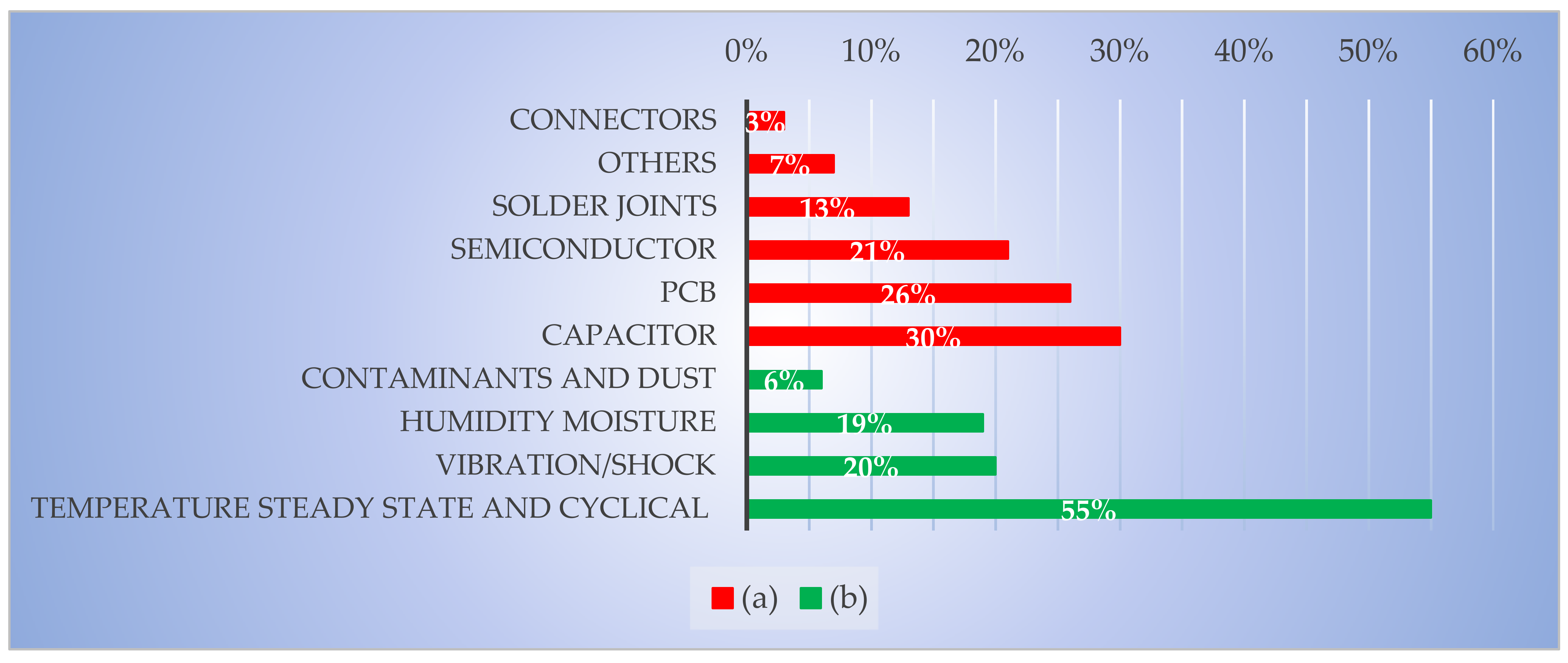
2.2. Preliminary Analysis of Capacitor Characteristics by Equivalent Circuit Model and Performance Comparison

A preliminary analysis of capacitor characteristics begins with characterizing a simple tantamount electrical circuit model that describes the equivalent series resistance (ESR), equivalent series inductance (ESL), and capacitance (C) that represent the capacitor’s respective physical characteristics [33]. The equivalent circuit model design depends on the type of capacitor, where there is a difference among the cases AE-C, MLC-C, and MPF-C as described in Figure 4. In addition, the equivalent circuit model also represents the insulation resistance R i (usually large), dielectric loss R d (significant at high frequencies), and inherent dielectric absorption C d (only significant in electrolytic capacitors). According to the equivalent circuit model, the capacitor impedance equation can be represented as:
Z c a p = R + j X = E S R 2 + 2 π f E S L 1 2 π f C 2  
A typical structure of an MLC-C comprises vertically stacked internal electrodes that form capacitive layers with dielectric substrate, and therefore the MLC-C-equivalent circuit model is different from the AE-C/MPF-C. The equivalent circuit model can be depicted as a π-model, which includes a total series impedance and two parallel impedances at each port output that have a common reference point as shown in Figure 4c. At the series impedance case (very similar to the case of a single layer), R 1 s , L 1 s , C 1 s , and G 1 s represent the total series resistance, inductance, capacitance, and conductance, respectively. In the parallel impedance case, the shunt effect between the capacitor and substrate (a major factor for the substrate effect) should be considered when placing the MLC-C on a board [34]. Therefore, the parallel impedance contains the resistance R s u b s in series, substrate capacitance C s u b , and the conductance G s u b . Where R s u b s represents a dielectric loss of bound electrons, the parasitic capacitance of the substrate and a small conducting loss of free electrons are referred to as C s u b and G s u b , respectively. Note that the paper presents a simple MLC-C first-order model and not a second-order model to avoid very laborious and cumbersome mathematical consequences.
The capacitor’s impedance vs frequency is a key parameter when designing a capacitor according to the application conditions. Therefore, based on an equivalent circuit model (Figure 4), a frequency response comparison of a 1 uF capacitor was performed among three cases: AE-C, MPF-C, and MLC-C as shown in Figure 5. The ESL value is generally neglected at lower frequencies ( ω L is small), below the self-resonant frequency, which is given by
f r e s = 1 2 π L C
Therefore, at low frequencies, the negative slope of Z is due to the dominance of the capacitive component ( Z 1 2 π f C ), termed as the capacitance component region. At the resistance component region (termed as resonance region), Z is represented by the ohmic resistance ( Z E S R ) only, and at higher frequencies, the inductive reactance begins to dominate ( Z 2 π f E S L ) that is termed as the inductance component region. Admittedly, in some cases, the simple electric capacitor model is not accurate enough (a significant factor in lifespan prediction and capacitor reliability). Therefore, if the goal of the design is to achieve an accurate model of the electrical capacitor as closely as possible, the parameter values of the capacitor model (resistance, capacitance, and inductance) are no longer constant values; these values should vary depending on environmental (humidity, temperature, etc.) and operating (current ripple, voltage stress, etc.) conditions.
When comparing the advantages and disadvantages among different types of capacitors, the first and most important factor to consider is the limit of storable energy ( W V ) per volume (in dielectric material). Equation (3) introduces the storable energy limit in a capacitor where E m a x is the maximum operating field strength, and ε r is the relative permittivity. Hence, the values of ε r and E m a x (dielectric material properties) are a major factor influencing the limit of storable energy per volume.
W V = ε 0 ε r E m a x 2 2
Figure 6 shows a diagram depicting the energy storage density values for various common dielectrics depending on relative permittivity and operating field strength [35]. From the energy storage density diagram, it can be clearly seen that A I 2 O 3 (AE-C material) has the highest energy density, in the range of 10 J / c m 3 (theoretical limit) to 2 J / c m 3 (commercially available limit). AE-C has this significant advantage, due to the high relative permittivity (10) and the highest field strength between 200   and   600 V / μ m . Despite this, polypropylene (MPF-C) contains a high-field strength of 200 V / μ m , but on the other hand, suffers from very low relative permittivity compared to ceramics (1500). Following the advantage (highest relative permittivity) that ceramic (MLC-C) has, it suffers from the lowest field strength, so the energy storage density of the ceramics and the polypropylene is almost equivalent, about ~ 0.2 J / c m 3 . Note that the biaxial-oriented polypropylene is the favored film material for applications above 250 V.
Table 1 shows relative performance comparisons of the three main capacitor types, AE-C, MPF-C, and MLC, for DC-BUS applications [36]. For example, as mentioned above, A I 2 O 3 has the highest energy density (up to about 2   J / c m 3 ); therefore, it has the highest capacitance per volume among the three. In addition, it also has the lowest cost per joule, but unfortunately, due to electrolyte evaporation, it suffers from low reliability; moreover, due to high-temperature sensitivity, it also suffers from relatively high ESR and low ripple current ratings (typical 20 m A / μ F ). Another disadvantage of the electrolyte is a low voltage rating (maximum 500–600 V) compared to MPF-C (from a low voltage to 50 kV) as can be seen in Figure 7. The capacitance range vs voltage range plot is an important parameter when choosing a capacitor according to a specific application, while the voltage and capacitance correlate with the physical size and cost. MPF-C presents the optimal parameters of all three types (mentioned above) in terms of the lowest ESR, lowest current ripples (typical 1   A / μ F ), and well-balanced performance for high-voltage applications. Despite a lower financial cost and relatively high capacitance (compared to MLC-C), it is limited to a moderate upper operating temperature, unlike the ceramic capacitor. Other advantages of MPF-C are high reliability and the highest flexibility in device geometry among all capacitor technologies, yet it suffers from a large volume problem due to the lowest energy density (up to about 0.15 J / c m 3 ) of the three types. MLC-C offers a high reliability, a wider frequency range (compared to A I 2 O 3 ), and the highest operating temperatures (up to about 200 C ° ) of all three types. Although MLC-C offers lower ESR and current ripples (compared to A I 2 O 3 ), ceramic capacitors have a much lower energy density than electrolyte capacitators (up to about 0.2   J / c m 3 ). However, the major disadvantages of the MLC-C are the high financial costs and mechanical sensitivity; these drawbacks are intensified in high-voltage applications.

3. Common Techniques for DC-BUS Capacitance Reduction Circuit Applications in Capacitor-Supported Power Conversion Systems

3.1. Introduction to DC-BUS Capacitance Reduction Circuit Applications

After presenting the problem of using electrolytic technology in power conversion systems in Section 1 and then equalizing the performance among the different capacitor technologies in Section 2, this section discusses common topologies and control strategies for DC-BUS capacitance reduction circuit applications and the replacement of electrolytic capacitors with other capacitor technologies. Many attempts to reduce DC-BUS capacitance and replace electrolytic capacitors are described in the literature. The approaches available in the literature for resolving the electrolyte capacitor issue of power converters and achieving capacitance reduction are shown in Figure 8. The most common solutions are (1) compromise of converter performance, (2) DC-BUS capacitance distribution, (3) ASC addition DC-BUS case, series connection with the converter side, (4) ASC addition DC-BUS case, series connection with the capacitor side, (5) ASC addition DC-BUS case, shunt connection, (6) ASC addition AC case, series connection, and (7) ASC addition AC case, shunt connection. The following is a brief description of the above techniques.
  • Compromise of converter performance: The converter performance is determined by an optimizing process of the DC-BUS capacitor selection shown in [38]. The maximum allowable DC-BUS VRs are then calculated for different types of applications as shown in [39,40,41], and thus by enhancing VRs over a DC-BUS, capacitance reduction can be achieved. However, this technique is less common due to its suitability for very specific applications that are not sensitive to increased VRs. Applying this technique in systems sensitive to VRs will directly cause a decrease in system performance and may even cause damage; therefore, this technique is not discussed in this paper.
  • DC-BUS capacitance distribution: the DC-BUS capacitance can be divided by an asymmetrical split of the DC-BUS capacitor into two smaller capacitors with a common connection point. The method is based on power flow routing control from the DC-BUS or AC grid to the capacitors by DC–DC converters. This technique is similar to the active capacitor equalization process [42,43,44].
  • ASC addition DC-BUS case, series connection with the converter side: the topology concept is based on introducing an energy source in series with the DC-BUS to compensate the VR on the DC-BUS capacitor and make the output voltage have a near-zero ripple by directing the pulsating portion of the instantaneous force into the auxiliary capacitor C A [45,46]. Thus, the total required capacity is reduced, and electrolytic capacitors can be substituted by alternatives with an extended lifetime and compatible or reduced volume and cost. The ASC connection is implemented by a bidirectional DC-BUS converter and ends with an auxiliary capacitor with a capacitance value significantly smaller than the required DC-BUS BEC C B .
  • ASC addition DC-BUS case, series connection with the capacitor side: The ASC unit is based on the same principle as the previous solution. However, the main difference among the methods is that in this case, the ASC unit is located in series connection with the DC capacitor across the DC-BUS [47,48]. Therefore, unlike the previous solution, the voltage ripple is reduced on both sides of the DC-BUS (AC/DC or DC/AC side). The ASC unit can be applied in full-bridge topology [49] or as a hybrid filter [50,51].
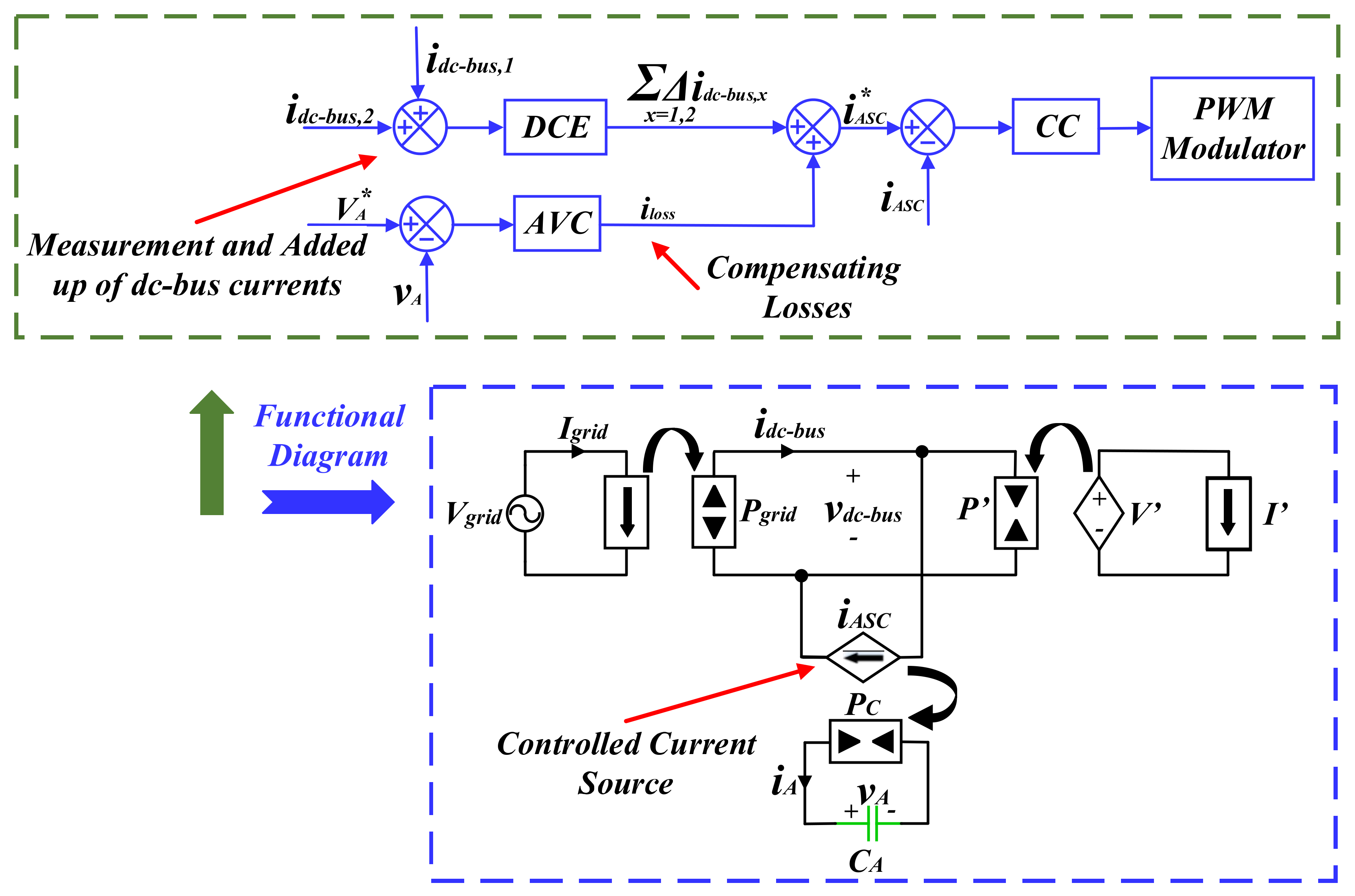
  • ASC addition DC-BUS case, shunt connection: this case is based on the same concept as the above technique, except for the ASC connection topology. The technique offers a shunt connection between the bidirectional DC–DC converter and the DC-BUS. Furthermore, in this case, at the converter output ports, there is an auxiliary capacitor C A with a capacitance value significantly smaller than the required DC-BUS BEC C B [52,53,54,55,56,57,58].
  • ASC addition AC case, series connection: In this case, the topology concept is based on introducing an energy source in series with the AC side, as shown in [59]. Similar to the DC-BUS case (converter side), this topology allows control of the VRs of the DC-BUS capacitor (by routing the energy flow across the capacitor) [60]. As a result, the DC-BUS capacitance requirement can be reduced, and a different type of DC-BUS capacitor can even be used, such as film or ceramic. Nevertheless, this solution is less popular and therefore not discussed in this paper.
  • ASC addition AC case, shunt connection: This solution introduces ASC integration in a parallel connection across the AC line [61]. The major benefit of this strategy is the achieved excellent simplicity to performance ratio, because no complex current reference computations are required. However, as in the previous case, this strategy is also unpopular and therefore not discussed in this paper.
The following subsections present an extensive breakdown of each technique separately, including an analysis of the most common control strategies for each topology, each technique’s advantages/disadvantages, and a summary.

3.2. DC-BUS Capacitance Distribution

3.2.1. DC-BUS Capacitance Reduction Circuit Applications in a DC–AC Inverter System

One of the methods for significantly reducing the DC-BUS capacitance requirement for DC/AC inverter applications is to split the DC-BUS BEC into two symmetrical capacitors and insert a common-mode (CM) conducting path into the converter’s neutral point. The technique is very common among energy conversion system applications between PV panels and the AC grid [62,63]. Efficient use of the CM path opens the possibility of controlling the injection of CM voltages ( C M V ) into the output filter capacitors, and thus a power oscillation buffer (pulsed power) can be applied between the converter output and the DC-BUS as shown in Figure 9 [64]. An additional benefit of the CM conducting path method is that the ground leakage current can be sufficiently well eliminated by ground leakage current control (enabled by the PV to ground parasitic capacitance). The topology is based on the introduction of new freewheeling routes into the converter; thus, the source chassis (e.g., PV panel) can be isolated from the output (e.g., AC grid) during freewheeling modes. This could be accomplished by interrupting the C M i conducting path when zero voltage vectors are employed to the full-bridge inverter either on the DC or AC side. However, the advantage of the ground leakage current control does not contribute to reducing DC-BUS capacitance and therefore is not detailed here.
The main advantage of this method is the ability to uncouple the well-known double-line-frequency pulsating power (that originated from the AC side) by further injection of C M V into the output filter capacitors. By this disconnection, the DC-BUS will not sense the second-order pulsating power, and the DC-BUS capacitance requirement will be significantly reduced. In such a case, the requirements for filtering the DC-BUS are increased compared to a standard H-bridge inverter due to the C M V injection, and this directly affects the filter capacitance value. Descriptively, if the compensation voltage factor ( V c o m p ) is satisfied, the second-order pulsating power in the AC network should be well filtered by the filter capacitors C f 1 and C f 2 ; thus the DC-BUS will not sense these power pulses. However, although the compensation voltage factor can be provided (theoretically), it remains impossible to decouple the entire AC grid-pulsating power, because the fourth-order harmony is added due to the computational interaction between the capacitor voltages and the current’s second-order terms. In addition, some other disturbances, such as passive component ESR, variation of the inductance and capacitance, internal filter pulsating power (due to the inductors), and distortions caused by dead time, are not calculated by this method. Therefore, it could be determined that a residual power ripple appears at the DC-BUS of the PV inverter, and the elimination of fluctuating power is incomplete. Undoubtedly, the advantage of this method is that it requires no auxiliary converter (or any switching components) and has a simple circuit configuration, while the main disadvantage of the method is the necessity for an additional current sensor, which makes plug-and-play operation inapplicable.

3.2.2. DC-BUS Capacitance Reduction Circuit Applications in AC–DC Rectifier System

One of the common methods for direct rectification applications from the mains to DC-BUS is a direct AC/DC differential rectifier that does not use an electrolytic capacitor and has a mitigated low-frequency ripple [65,66]. The presented technique is based on a single-stage direct AC/DC rectifier with no need of an electrolytic capacitor, by using inductor current waveform control methodology [67]. The concept is based on two bidirectional DC/DC converters for AC/DC rectifiers replacing a standard PFC converter. The bidirectional DC/DC converters are series-connected at the input terminal, while the output nodes are in parallel connection to the DC-BUS. In this topology, the electrolytic capacitor was replaced by two capacitors C 1 and C 2 , while their voltage drop has an opposing polarity ( V c 1 and V c 2 , respectively), and the difference is a pure sinusoidal waveform that follows the input AC source shape.
The presented topology utilizes two bidirectional buck–boost power converters connected in the differential configuration as shown in Figure 10; nevertheless, a variety of converters, such as buck–boost, flyback, push–pull, and forward, can also be suitable here. The upper buck–boost is formed by C 1 , Q 1 , Q 2 , and L 1 (upper side), and the lower converter is formed by C 2 , Q 3 , Q 4 , and L 2 (lower side). In a complete AC cycle, the four feasible states ( S 1 S 4 ) of the buck–boost differential are applied to switches Q 1 Q 4 . The switch state operation is as follows: S 1 : Q 1 OFF; Q 2 ON; Q 3 OFF; and Q 4 ON where S 3 is its reverse state of S 1 . In states S 2 : Q 1 OFF; Q 2 ON; Q 3 ON; and Q 4 OFF where S 4 is its reverse state of S 2 . The operation of the buck differential rectifier is as follows: In the positive half cycle, the possible states are S 1 , S 2 , and S 3 ; and in the negative half cycle, the potential conditions are S 1 , S 3 , and S 4 . The presented method is aimed to mitigate the unbalanced instantaneous double-line-frequency input power with the constant output power demand. For example, in the positive half cycle, the upper buck–boost converter delivers more power than required at the dc side. To maintain constant output power, the superfluous energy is accumulated in C 2 . Thus, the lower buck–boost converter is only sinking power from the DC-BUS side ( Q 1 ON, Q 3 ON, and S 3 modes). This process applies to both half-cycle modes (positive and negative) in the same way and is physically inevitable.
For the presented differential rectifier system, a general control technique for mitigating the double-line-frequency power at the DC side of the circuit for implementing a free electrolytic capacitor system is proposed. Due to the series connection of C 1 and C 2 , their differential voltage is equal to the AC line voltage v a c t = v c 1 t v c 2 t = V m sin ω t . In this case, the output current i o t will contain a double-line-frequency component i o 2 ω . Thus, the input capacitors C 1 and C 2 filter only the high-frequency harmonics. When expending the control bandwidth to cover the double-line-pulsating power, the capacitors can filter it too; hence, the DC line capacitance could be reduced. Consequently, the existing systems without any hardware modification prolong the system’s lifetime by a slight change of the control methodology, which is a significant advantage of this method. Nevertheless, the fourth current component i o 4 ω cannot be eliminated; this component will eventually manifest as output current ripples. However, because these current ripples are typically very low, only a small non-BEC is required for eliminating all ripple current harmonic components at the DC-BUS. The main disadvantage of this method is the multiplicity of the switching components and inductors. For example, a typical boost PFC converter is implemented by a single switch and inductor, instead of four switches and two inductors offered in the above method. This disadvantage can impair the converter’s functionality in a variety of ways, such as high cost, complexity of the power stage, and high probability of future failure due to increased switching components.

3.3. ASC Addition DC-BUS Case, Series Connection with the Converter Side

An auxiliary voltage source in series connection with the DC-BUS is an applied technique for reducing the required capacitance of the power conversion system [68,69,70]. This method has been successfully implemented in typical PFC front-end power conversion systems [71]. The concept is based on connecting a serial voltage compensator circuit between the DC-BUS BEC and the load. By utilizing the voltage compensator circuit, the system energy storage is reduced, enabling to utilize lower capacity in a higher performance device. From a power-balancing point of view, the load current flows throughout the auxiliary circuit, where it processes only the reactive power, and the output terminal voltage is AC. Because the voltage compensator circuit processes small VR, the reactive power element has a low power rating. Therefore, the use of a voltage compensator circuit in general capacitor-supported power electronic systems has several major advantages, such as implementation that requires low-voltage devices only, ability to increase the VR in DC-BUS BECs (which is beneficial for power balancing between the line and load), and reduction of the DC-BUS capacitance requirements.
The basic concept of implementing a voltage compensator circuit for a typical energy conversion system [72] is illustrated in Figure 11a. The model consists of a DC-BUS shared by two cascade converters, where C is the capacitor, and V a b represents the auxiliary voltage source as illustrated in the voltage compensator circuit. The capacitor voltage v C can be separated into two parts: a constant voltage component V C and a VR component v c , where the capacitor ripple fluctuates at f r i p , and the peak to peak ripple is 2 v c . The auxiliary voltage source ( V a b ) is connected between the DC-BUS capacitor positive port and the SSIC positive node. The auxiliary voltage source produces a voltage opposite to the VR component of the DC-BUS capacitor where V a b = v c (i.e., DV component tends to zero). At the nominal point, v d has an identical average voltage value as at the DC-BUS capacitor (with zero VR). Therefore, a high VR across the DC-BUS capacitor C is allowed, indicating that the capacitor value can be reduced, but at the expense of increasing the magnitude of v a b .  Figure 11b illustrates the voltage compensator circuit, which is based on four low-voltage MOSFETs Q 1 Q 4 and a DC–AC full-bridge inverter with an output filter L f C f . The switch gate signals P W M 1 P W M 4 in the full-bridge inverter are generated by a PWM. Depending on the type of DC source used, the control signal v c o n is obtained by sensing different parameters. When utilizing the unidirectional current flow from the line to the load, a couple of switches could be applied by diode (e.g., Q 2 and Q 3 or Q 1 and Q 4 ), as in a standard half-bridge circuit.
A series auxiliary voltage source circuit can be integrated into a variety of capacitor-supported power electronic systems. A good example of adding an auxiliary source in series with the DC-BUS is the implementation of a voltage compensator circuit in photovoltaic (PV) systems. Figure 12a shows a circuit diagram of a grid-tied solar inverter with a series voltage compensator circuit for reducing the high-voltage DC-BUS capacitance based on a capacitor-supported full-bridge DC–AC converter. The voltage compensator circuit is connected in series to the DC-BUS (power processing side) between the input DC–DC boost converter (PV side) and output DC–AC inverter (grid side) [73]. The voltage compensator circuit, DC–DC boost converter, and the DC–AC inverter, are highlighted on the circuit diagram with red, green, and pink backgrounds, respectively. The compensator circuit generates an AC voltage that counteracts the VR on the output terminals of the boost converter. Therefore, the grid-tied inverter-supplied voltage is equal to the capacitor C d c b u s average voltage. Thus, in this case, the compensator processes an AC power only, which fluctuates at double the speed of the line frequency. The main controller interface (DSP-based) is presented in Figure 12b, where the subcontrol circuits of the PV boost converter, series voltage compensator circuit, and inverter are highlighted in green, red, and pink, respectively.
The series voltage compensator control circuit operation is attached as follows: First, a sample of v a (auxiliary capacitor voltage) and v d c b u s (DC-BUS voltage) is performed, where α (scaling factor) is the ratio between the triangular carrier signal amplitude in the PWM modulator and V a , r e f ; where V a , r e f is the voltage reference for the input voltage compensator circuit V a b . The PI controller ( G s ) processes the gap between V a , r e f and v a to give an offset voltage v o f f s e t ; then, the v o f f s e t and α signals undergo a summation operation, and a control signal v c o n is obtained. At nominal operation, v o f f s e t   cancels v c o n and the α v d c b u s DC component as V o f f s e t = α v d c b u s   (where V o f f s e t expresses the DC component of v o f f s e t , and where V d c b u s expresses the DC component of v d c b u s ). The signal v c o n is diverted to the PWM modulator and generates the voltage v a b that has the same phase and amplitude as Δ v d c b u s , and finally the PWM signals are directed to switches Q 1 ~ Q 4 . Note that for following the cancellation of the α v d c b u s DC component, it is not necessary to use an HPF filter to isolate the AC component from v d c b u s ; consequently, by voltage control, a stable DC level of v a can be achieved. Therefore, this control technique ensures that the voltage compensator circuit only handles the reactive power in the steady state, meaning v c o n equals the conditioned AC component of α v d c b u s in steady-state operation.
To summarize, the series voltage compensator circuit topology can be realized by a DC–AC converter with a full-bridge circuit; in the case of a unidirectional current flow of i d , a half-bridge topology is an appropriate solution. In addition, the DC-BUS capacitor selection is no longer set by the VR value ( V d ), but instead by the designed allowable voltage stress on the auxiliary capacitor C a . There are several options for DC-BUS capacitor selection in this configuration due to the DC-BUS capacitor’s ability to withstand low-voltage stress. One of the alternatives is to utilize a long-life, high-ripple, low-voltage electrolyte capacitor because they are a very common and cost-effective solution. Another option is to employ a low-voltage film capacitor or ceramic capacitor tank. The main advantage of this technique is the that it allows to implement the auxiliary voltage compensator circuit with very low-voltage switching devices and passive elements, because the compensator processes small VR on the DC-BUS and therefore only the reactive power element. Another advantage of this technique is reducing the capacitance value, which correlates with the input–output power balancing; thus, the DC-BUS VR will increase. In addition, by the possibility of high VRs across C , the capacitance value can be reduced but at the expense of increasing the magnitude of v a b . Despite the advantages mentioned above, this technique has several major drawbacks: (a) A simple fault in the voltage compensator circuit disables the entire system, due to the auxiliary converter’s connection in series to the DC-BUS. This disadvantage significantly reduces the energy conversion system’s reliability. System reliability is a key factor when designing an energy conversion system, and, as a result, this technique is not common in energy converter applications. (b) This technique is not applicable on existing grid-connected power conversion systems due to the series connection in the voltage compensator circuit, which requires some hardware modifications; thus, the plug-and-play operation cannot be applied. (c) Application complexity: due to the multiplicity of components, a more cumbersome structure and more complicated control circuit are obtained. (d) In the proposed arrangement, the voltage compensator circuit is located between the DC-BUS capacitor and one of the converters (FSIC or SSIC) only. Therefore, always one side is suffering from a lack of stress regulation. (e) Voltage swing limits across the capacitor due the converter (FSIC or SSIC) operating voltage.

3.4. ASC Addition DC-BUS Case, Series Connection with the Capacitor Side

As in the previous solution, the technique here is based on inserting an ASC into the DC-BUS by series connection topology, but the difference is in the ASC location. The above technique offers a series connection between the DC-BUS capacitor and the ASC unit as shown in Figure 13a. The research in [74] presents a high-power-density buffer with high-efficiency performance. This technique offers an appropriate solution to two main requirements when combining an ASC on the DC-BUS system (for pulsating power elimination): the first is energy storage capability and the second is DC voltage regulation. The DC-BUS capacitor energy storage problem arises due to a permissible VR limit on DC-BUS systems, and only a minimal part of the capacitor energy stored is utilized; e.g., for a 3% VR limitation across the DC-BUS, the energy buffering ratio is approximately 6%. Therefore, the first requirement solution is based on adding a DC/DC converter, which is a buffer between the auxiliary capacitor and the DC-BUS; thus, the auxiliary capacitor is no longer subject to the rigid limitations of VRs. Like the preceding case, the series connection benefit over the shunt connection (Section 3.5) is the ability to process only reactive power. By processing a small VR only, the reactive power element has a low power rating, and the ASC unit can be applied by low-voltage devices. While the previous technique suffers from a reduced VR on just one DC-BUS side and voltage swing limits across the capacitor due to the converter operating voltage (FSIC or SSIC), this research presents an integrated solution to the above problems. By placing the ASC unit in a series connection with the DC capacitor across the DC-BUS, the problem of the reduced VR on only one side is solved, and the voltage swing limit problem is also solved directly due to the series connection topology.
The ASC unit is implemented as a bidirectional current source to balance the instantaneous current gap between the AC and the DC current and consists of a DC–DC -bridge converter ( Q 1 ~ Q 4 ), inductor ( L f ), capacitor ( C f ) for filtration, and auxiliary capacitor ( C A ) as shown in Figure 13b. C b u s is a small filter capacitor to absorb the switching transients; therefore, its effect is negligible. The bidirectional current source is stacked in series with the major energy storage capacitor C 1 ; thus, it allows a relatively large VR over C 1 to increase its energy utilization ratio. For example, instead of a maximum VR of 5~8% (a typical case of V b u s = 400   V ) across C 1 , the VR can be increased to over 20% of the nominal voltage. For the ASC to behave like a current source, there is a need to design a current control strategy so that the V a b will naturally vary contrarily to the variable voltage of C 1 (i.e., V C 1 + V a b = constant). In fact, because the sum of the instantaneous current gap of each double-line-frequency cycle is zero, automatic energy balancing is performed in each cycle, and the buffer converter does not need a C A   to fulfill its current source function. The control strategy purpose in this research is to force the ASC unit to behave as a controlled current source. Therefore, it is critical to precisely control i b a f f (instantaneous current gap between the AC and the DC current) in order to keep the V D C B U S as constant as possible. The required i b a f f value is equal to the AC component of the AC side, because i D C   s i d e and i A C   s i d e have the same average value. First, as shown in Figure 13c, the value of i A C   s i d e is measured and passes through a BPF (to obtain the double-line-frequency component only) to use as feedback for i b a f f . The BPF can be divided into two parts: a digital moving average filter and LPF in the analog sensing circuit. To evaluate the DC component only, a microcontroller is used to obtain a moving average filter at 120 Hz (creates an HPF to eliminate the DC component), and the LPF in the analog sensing circuit is for filtering the SSIC switching ripples.
The insertion of an ASC in a series connection with the capacitor side offers a high-efficiency and high-power-density buffer for pulsating power elimination. This technique offers a variety of benefits, such as (a) small DC-BUS VRs, (b) implementation by very low-voltage switching devices and passive elements, and d) reduced VR on both sides of the DC-BUS (FSIC and SSIC). On the other hand, this technique suffers from several drawbacks, such as (a) additional BEC for topology realization is required; (b) similar to the previous solution, the plug-and-play operation cannot be applied on an existing system without hardware modifications; and (c) application complexity: due to the multiplicity of components, a more cumbersome structure and a more complicated control circuit are obtained.

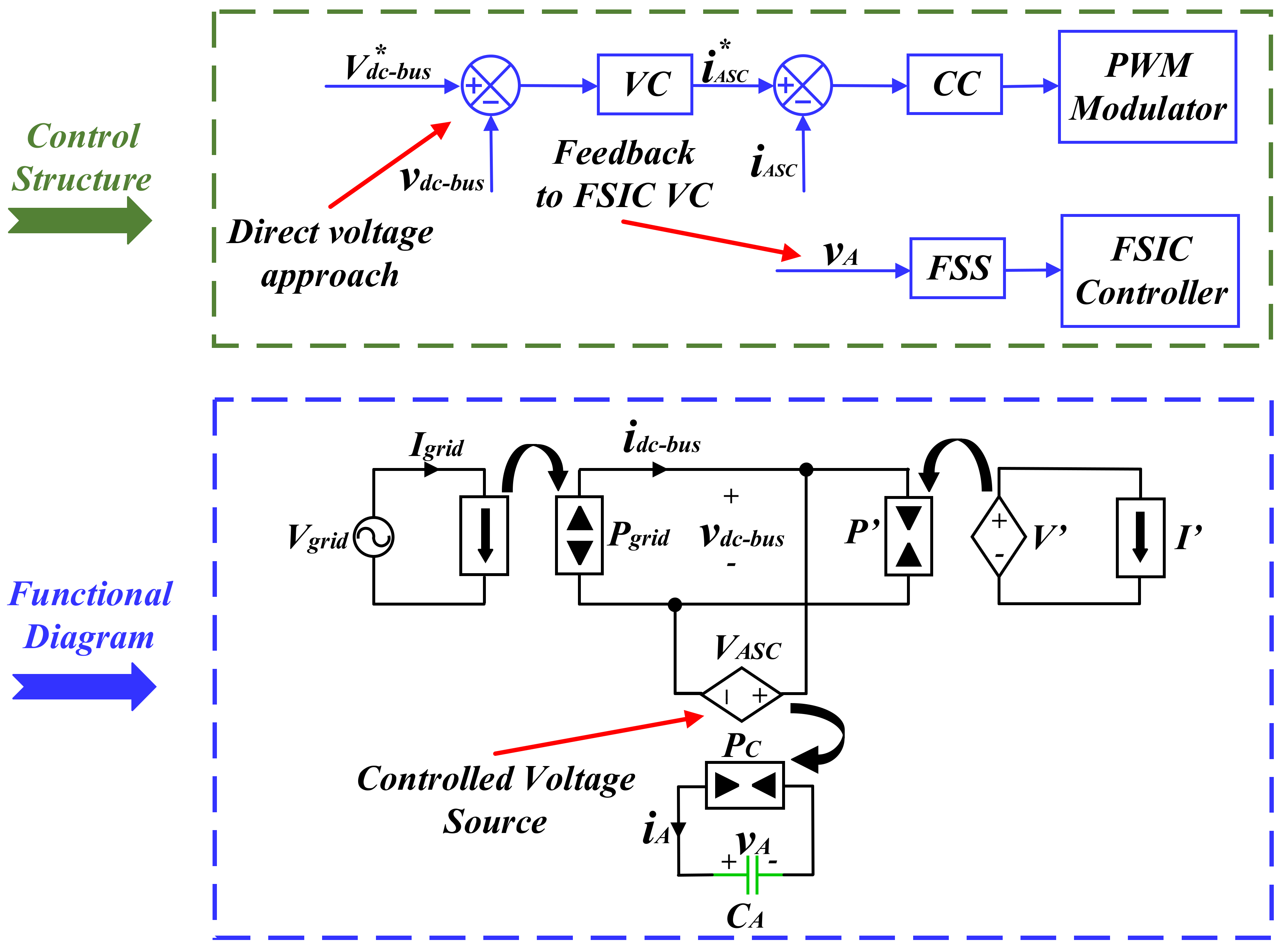
3.5. ASC Addition DC-BUS Case, Shunt Connection

3.5.1. Basic Principle of ASC

The existing literature describes several techniques for reducing the capacitance utilized in a power conversion system and presents comparisons among the different techniques to estimate the minimum capacitance needed for ASC applications [75]. Among them, adding an ASC in shunt connection is probably the most popular one. The principle of operation of these circuits is based on replacing a bulky and low-reliability DC-BUS electrolyte capacitor with a bidirectional DC–DC converter that contains an inductor and two switches and ends in a much smaller auxiliary film capacitor C A as shown in Figure 14. The offered technique has many uses, and each application has advantages/disadvantages for different system purposes. An example of using an ASC addition in shunt connection is applying the auxiliary source as a DC-BUS-pulsed power load filter, as reported in [76,77]. The principle of the operation of such systems is based on an input/output power balance between the source interface and the load interface. The concept is implemented by adding an energy source (capacitor/supercapacitor) in parallel to the DC-BUS via a bidirectional DC–DC converter. Nevertheless, the target of these systems is to filter the pulsating of the load’s power demands (Pulsed Power Supply application) and not to implement DC-BUS capacitance reduction or DC-BUS ripple eliminators. The presented pulsed power filter in [78] shows a DC-BUS capacitance reduction but does not eliminate the DC-BUS ripples and does not support the plug-and-play operation, because the control scheme requires an access to the corresponding load current. In addition, it is designed for special load profiles; therefore, these methods are not discussed in this paper.
This subsection’s purpose, rather, is to collect and introduce major methods for applying the above technique, while analyzing results and presenting advantages and disadvantages. This method performs collection by focusing on the main requirements of power conversion systems, such as reduction of DC-BUS capacitance requirements, eliminating DC-BUS ripples, and enabling plug-and-play operation. The DC-BUS ripple eliminators circuit family and DC-BUS capacitance reduction capability have been offered in [6,79]. The ripple eliminator circuit can be divided into three categories based on different control strategies: controlled current source (active power filter-based), controlled voltage source (direct voltage regulation-based), and capacitor dynamic behavior imitation (infinite capacitor). These control methods are common among ASCs in the shunt connection and therefore should be expanded upon.

3.5.2. Controlled Current Source Strategy (Active Power Filter-Based)

Extensive use for implementing an active filter-based control technique is found in the literature [80,81,82,83]. This control strategy is similar to the active power filter (from DC-BUS point) and operates as the current-controlled current sinks. The basic principle is sampling the total DC-BUS current pulsating component and designating it as control feedback, thus allowing DC-BUS capacitance reduction. In fact, in this technique, the ASC is implemented as a controlled current source toward the DC-BUS. Figure 15 illustrates the control structure and functional diagram of the regulated current source strategy. First, the control technique is based on measuring and summing up the DC-BUS currents ( i d c b u s   1 ,   2 N ); then, only the pulsating current component is obtained by the DC eliminator (DCE), and the obtained value i d c b u s ,   x is used as the DC-BUS current reference (directly or indirectly). Next, the loss-compensating term i l o s s t (generated by the auxiliary voltage controller) is added to the DC-BUS current reference; it is a necessary operation because the ASC is not ideal. Finally, the ASC switch signals are set by the current controller (CC). Note that between the CC and the ASC switches, there is a PWM modulator unit. As a result, the DC-BUS voltage is indirectly regulated by diverting all the pulsating current components into C A . Due to the control strategy requirement for measuring the currents, the current sensors are needed as well as access to measurement points outside the ASC. Therefore, this control strategy cannot operate in a plug-and-play approach. This disadvantage is even more noticeable if there are N converters connected to the DC-BUS. In this case, it is necessary to install N current sensors and corresponding measurement points. Another disadvantage of this control strategy is the additional delay that enters the system due to the DCE.

3.5.3. Controlled Current Source Strategy (Active Power Filter-Based)

Many ASC control strategies based on direct voltage regulation have been investigated as described in [84,85,86], and in this case, the control strategy operates as voltage-controlled current sinks. In fact, in this technique, the ASC is implemented as a regulated voltage source toward the DC-BUS, Figure 16 ( V d c b u s * ) voltage controller (VC)–CC. In this strategy (unlike the previous one), the pulsating current component is displaced into the ASC only by using information regarding the DC-BUS voltage and without external current measuring. This is a great advantage over the other methods, due to dispensing with DC-BUS current measurements; thus, adding current sensors is not required, and only DC-BUS voltage sensing is required.
Unfortunately, the system’s active power balance indicator does not function when the DC-BUS voltage is under tight regulation. Thus, when the auxiliary capacitor absorbs the pulsating power component, v A and v d c b u s no longer reflect the system’s power balance. In such a case, the FSIC voltage control loop should utilize v A as the controlled variable instead of v d c b u s . This means that v A must be the state variable of FSIC VC after appropriate filtering, shifting, and scaling (FSS). The consequence is that implementation of this control strategy also does not allow operation in the plug and play mode. When the VRs are eliminated, the ASC is an infinite capacitor as reported in [87]. However, in this case, system power balancing is no longer indicated at the capacitor terminals, additional feedback of v A is required, and operation in the plug-and-play mode is impossible.
The ASC control strategy of direct voltage regulation was proposed in [88,89]. These techniques enable a plug and play operation because the capacitor ripple voltage is regulated to zero by extracting the ripple component from the capacitor voltage. Figure 17 illustrates the control structure of the controlled voltage source strategy based on plug-and-play operation. First, only the v d c b u s is measured, and after that the pulsating component is solely obtained by DCE. By utilizing multiresonant VC, the residual pulsating elements are regulated to zero. At the same time, in this arrangement as well (as with a controlled current source) the loss-compensating term i l o s s t is added (an additional voltage loop closed across v A ). Finally, the ASC switch signals are set by the current controller. In this case (unlike the previous technique), the average bus voltage preserves its value, yet it could be utilized as an indicator for system power balance by FSIC VC; i.e., no extra FSIC voltage control loop is required, so the plug and play operation can be implemented by this technique. However, this technique is, likewise, based on DCE; thus, this system will also suffer from additional delays that enter the system. Another drawback of the proposed technique is the requirement for additional data related to the pulsating element frequencies or the base frequency that are necessary for designing a multiresonant controller.

3.5.4. Capacitor Dynamic Behavior Imitation Strategy (Infinite Capacitor)

Like the previous one, this strategy is also based on direct voltage regulation, but the difference of the Capacitor Dynamic Behavior Imitation (CDBI) approach from its predecessors (active power filter and direct voltage regulation) is that the ASC model is forced to imitate the dynamic capacitor’s behavior toward the DC-BUS as shown in Figure 18. Much research is reported in the literature on ASC applications based on the capacitor dynamic behavior imitation; for example, [90,91,92,93,94] discuss the functional operation of an electronic capacitor based on an ASC that imitates the capacitor behavior. In this case, there is no requirement to decrease the voltage ripple below a specific value (for example, below the ripple existing in a system based on electrolytic capacitance). While reducing the DC-BUS capacity requirement, one of the benefits allows plug-and-play operation; in such a case, it is essential to mimic the dynamic behavior of the replaced bulky capacitor. The VC of the converters (FSIC/SSIC) that are responsible for system power balancing are tuned according to the value of the originally utilized capacitor. Hence, it is important to regulate the ASC to function as a capacitor (from the DC-BUS point of view) to conserve the system’s low-frequency dynamics while utilizing the initial capacitor. This would inevitably allow the plug-and-play process. The ASC control strategy approach is based on a voltage regulation technique to overcome its main drawbacks. The first one is additional system delay (created by using DCE) and the second is information that is required for designing the multiresonant controller, such as data about the frequency bases or the pulsating frequency components. The main difference between these approaches is that as an alternative for regulating the DC-BUS voltage to a constant value V d c b u s * , the reference signal is time-varying, calculated from the DC-BUS side ASC input current according to Equation (4).
v d c b u s * t = 1 C A S C * i A S C τ i l o s s τ d τ
The dynamic capacitor imitation control structure can be divided into three subsystems as shown in Figure 18. The first subsystem is loss compensation. Loss-compensating term i l o s s t (generated by the auxiliary voltage controller) is added to the DC-BUS current reference. When considering a loss-free system operating at a steady state, the calculated i l o s s τ is equal to zero; therefore, as long as v d c b u s = v d c b u s * t , the ASC performs as a capacitor C A S C * . Furthermore, the AVC is added to maintain the system’s power balance (via i l o s s t ) because C A S C is a virtual capacitor, and pulsating power components are still displaced into C A . In fact, this is the main contribution of this research compared to its predecessors. The second subsystem is capacitance emulation; it implements Equation (4) to create the desired v d c b u s * , acting as converter output voltage reference signal, while the emulated capacitance could be time-varying. The third subsystem is CV/CC control and forces the bus instantaneous voltage V to tightly follow the reference v d c b u s * by processing the tracking error through standard CV/CC controllers and running the converter switches accordingly. This research has been developed and extended to many applications based on ASC circuits in a shunt connection, such as a two-stage power conversion system based on the DC-BUS for interfacing photovoltaic generators with AC mains [95] and improving the control structure of the electronic capacitor [96].
Other comprehensive research papers dealing with ASC applications based on the capacitor dynamic behavior imitation are presented in virtual infinite capacitor (VIC) research [97]. The VIC approach is defined as a nonlinear capacitor in which for an interval of the charge Q (the operating range), the voltage V ( V r e f ) remains steady. The dynamic capacitance C at a given point Q could be defined by 1 C = d V d Q ; thus, the energy accumulated by the capacitor during an infinitesimal change of charge ( d Q = i d t ) as: d E = V d Q . Therefore, a nonlinear capacitor at any voltage V Q has a flat region, namely d V d Q = 0 for Q Q m i n ,   Q m a x , named VIC. The Q–V curve shown in Figure 19 illustrates the operation area of Q as V r e f remains constant. While capacitor voltage dependence V (in a typical case) on Its stored charge Q is linear, as shown in Equation (5), the VIC offers an ASC that performs an imitation of nonlinear capacitor behavior.
Q t = 0 t i τ d τ
The principle of the VIC control operation is based on two controllers, a voltage controller (acts fast to maintain the desired terminal voltage) and charging controller (acts more slowly and may regulate the incoming current in the low-frequency range; thus Q remains in the desired range). Figure 20 presents the VIC control structure; a detailed control process explanation is found in [97]. Note that the VIC has become more efficient in [98] with lossless zero-voltage switching realization, and a variety of VIC-based ASC applications can be found on the capacitor-supported power conversion system, such as MMCs, wind turbine systems, and PFCs in [99,100,101].
However, because Q cannot be evaluated from V in the useful operating range, having an infinite capacitor feature at the ASC requires additional measurement for the Q revaluation (meaning an additional output). In the above area, the dynamic capacitance is infinite, but the quantity of stored energy (the left region of the Q–V curve) is restricted and not very large. Therefore, this method is recommended for use as a voltage regulator or filter capacitor (DC-BUS voltage ripple elimination) but is not intended for energy storage. The major drawback of this control method is that the reference voltage is fixed ( V r e f is a constant value). To ensure that the DC-BUS voltage reaches an equilibrium exactly at this value, the charge controller of the VIC must be integrated with the FSIC. Therefore, even in this case (as in direct voltage regulation), the system power balance is no longer indicated by the bulky capacitance, and additional feedback of auxiliary capacitance voltage is necessary. As a result, this disadvantage prevents the plug-and-play operation benefit. Following the above method, the research was expanded, and the VIC control has been improved in [102]; the new algorithm regulates the VIC reference voltage instead of forcing the bus voltage to follow the reference signal. The proposed control algorithm allows to connect the VIC directly to the DC-BUS in the same way as a passive capacitor; therefore, in this case, plug-and-play operation is applicable. Note that this work is a breakthrough for much of the VIC-based research that allows plug-and-play operation, including a significant reduction of DC-BUS ripples to a very low level by an improved control method [103,104], modular realization of the active capacitor [105], and electric vehicle (EV) charger applications [106].

4. A Detailed Analysis and Comparison of the Available ASCs

Recently, the integration of ASCs in capacitor-supported power conversion systems has attracted the attention of researchers due to its high reliability and appropriate power quality. Moreover, the integrated ASC provides benefits, such as a reduction of cost, weight, and size of the conversion stage. The use of a compact ASC abolishes the use a bulky electrolytic capacitor and can even be implemented as a source of energy bursts supply for pulsating loads. Many topologies of ASCs already exist (as presented in Section 3) for the benefits mentioned above, but researchers are still developing a new version of ASC topology for a variety of advantages in different applications. The presented topologies throughout the paper can be classified into five solutions: DC-BUS capacitance distribution (passive), DC-BUS capacitance distribution (active), ASC series connection with the converter side, ASC series connection with the capacitor side, and shunt connection. The differences among the topologies can be diagnosed by five criteria as shown in Table 2: Converter Rating, Current, Voltage Stress, Simplicity of Topology/Component Count, and Control Effort. The converter rating at DC-BUS capacitance distribution solutions is in a cascade connection; thus, the rating is with full energy, and the ASC solutions process only the pulsating power; therefore, they demonstrate top performance over other solutions. In terms of current, the shunt connection and series connection (capacitor side) topologies process the smallest current value due to the DC-BUS parallel topology. In the series connection case, the ASC handles only the ripple voltage across the DC-BUS; therefore, it has the lowest voltage stress. Undoubtedly, the shunt connection has the simplest topology due to the low component count and plug-and-play capability. On the other hand, due to the CDBI requirement, the control effort in the shunt connection solutions is the highest.
Nowadays, the main contribution of the ASC is a reduction of the DC-BUS capacitance requirement, eliminating the DC-BUS ripples, filtering the powering pulsed power loads, and finally, allowing plug-and-play operation (major benefit). The selection of the appropriate topology for a specific application is challenging because every topology has its own pros and cons depending on the implemented control strategy. Therefore, the selection of the topology for a particular application is based on the control strategy and topology structure as a detailed comparison in Table 3. In addition, the DC-BUS capacitance reduction circuit topologies are reviewed based on the three different categories: DC-BUS capacitance distribution, addition of a supplementary source, and series/shunt connection configurations. In the case of the DC-BUS capacitance distribution topology, there is no need to add an auxiliary storage. This advantage confers greater circuit simplicity compared to other topologies, by slightly changing the control strategy. Series connection topology provides an option to implement the ASCs with very low-voltage switching devices and passive elements, due to the small ripple voltage on the DC-BUS and reactive power only. However, shunt connection configurations have the highest reliability and efficiency compared to the rest, and therefore, it is also the most dominant configuration. Furthermore, this structure (not all control strategies support this option as shown in Table 3) allows plug-and-play operation compared to the series connection. This section’s purpose is to summarize all the main techniques for optimizing capacitor-supported power conversion systems and to present the advantages and disadvantages of each topology relating to the selected control strategy.

5. Conclusions

The capacitor-supported power conversion systems with ASCs are used extensively in distributed generation systems to eliminate the need for BECs. Optimal ASC design and the use of a proper control strategy in these converters have paramount importance to increase efficiency, improve performance, and achieve high reliability in the power conversion process. Therefore, this review paper has largely focused on the reduction of DC-BUS capacitance by utilizing circuit topologies under four different common solutions, such as DC-BUS capacitance distribution, ASC series connection with the converter/capacitor sides, and shunt connection. In each solution, several control strategies that have been developed are identified in the literature and presented with highlighted information. In addition, a separate comparison is made for each technique as shown in Table 3 with an emphasis on its parameters and remarks. ASC solutions with the features of high reliability, appropriate power quality, plug-and-play operation, low price/weight, and reduced conversion stage size are always expected. Nevertheless, there is no such thing as a free meal. Each energy storage source, topology, and control strategy has its pros and cons, and therefore, a performance comparison among the different uses is necessary. Reviewing the available techniques for a DC-BUS capacitance reduction circuit reveals that shunt connection ASCs based on CDBI control are the most common solution due to their highest energy density, lowest converter rating, and plug-and-play operation. Still, the literature is poor in discussing the integration of ASCs with power converters feeding dynamic loads (e.g., pulsating load) that support plug-and-play operation. Future research within this subject will greatly contribute toward the integration of ASCs in various dynamic applications. It is expected that this review will be a helpful reference on ASCs for researchers, design engineers, and manufacturers who are seeking reliable power converters.

Author Contributions

Conceptualization, I.A. and N.A.; methodology, I.A. and A.K.; software, N.A., A.Z. and P.S.; validation, I.A., N.A. and A.K.; formal analysis, I.A.; investigation, N.A.; resources, I.A.; data curation, N.A.; writing—original draft preparation, N.A and I.A.; writing—review and editing, I.A.; visualization, N.A.; supervision, I.A. and A.K.; project administration, I.A. and A.K.; funding acquisition, I.A. and A.K. All authors have read and agreed to the published version of the manuscript.

Funding

The research was partially supported by the Israeli Innovation Authority (Grant number 75056).

Institutional Review Board Statement

Not applicable.

Informed Consent Statement

Not applicable.

Data Availability Statement

Not applicable.

Conflicts of Interest

The authors declare no conflict of interest.

Abbreviations

The following abbreviations and nomenclatures are used in this manuscript:
BECBulky Electrolytic Capacitor
ASCAuxiliary Source Circuit
FSICFirst-Stage Interface Converter
SSICSecond-Stage Interface Converter
VRVoltage Ripple
ESREquivalent Series Resistance
ESLEquivalent Series Inductance
AE-CAluminum Electrolytic Capacitor
MLC-CMultilayer Ceramic Capacitor
MPF-CMetallized Polypropylene Film Capacitor
BOPPBiaxial-Oriented Polypropylene
C B Bulky Capacitor
C A Auxiliary Capacitor
CMCommon Mode
C M V CM Voltage
C M i CM Current
R p Insulation Resistance
R d Dielectric Loss
C d Inherent Dielectric Absorption
W V Limit Storable Energy
PFCPower Factor Correction
PWMPulse Width Modulation
DSP Digital Signal Processing
HPFHigh-Pass Filter
LPFLow-Pass Filter
CCSControlled Current Source
CVSControlled Voltage Source
CDBICapacitor Dynamic Behavior Imitation
DCEDC Eliminator
CCCurrent Controller
CVVoltage Controller
FSSFiltering, Shifting, and Scaling
AVCAuxiliary Voltage Controller
VICVirtual Infinite Capacitor
PI Proportional Integral
EVElectric Vehicle
V c o m p Compensation Voltage Factor
f r i p Ripple Frequency
i l o s s t Loss-Compensating Term
MMCModular Multilevel Converter

References

  1. Haghbin, S.; Lundmark, S.; Alakula, M.; Carlson, O. Grid-Connected Integrated Battery Chargers in Vehicle Applications: Review and New Solution. IEEE Trans. Ind. Electron. 2013, 60, 459–473. [Google Scholar] [CrossRef]
  2. Gazafrudi, S.M.M.; Langerudy, A.T.; Fuchs, E.F.; Al-Haddad, K. Power Quality Issues in Railway Electrification: A Comprehensive Perspective. IEEE Trans. Ind. Electron. 2015, 62, 3081–3090. [Google Scholar] [CrossRef]
  3. Zhong, Q.; Zeng, Y. Control of Inverters Via a Virtual Capacitor to Achieve Capacitive Output Impedance. IEEE Trans. Power Electron. 2014, 29, 5568–5578. [Google Scholar] [CrossRef]
  4. Natarajan, V.; Weiss, G. Synchronverters with Better Stability Due to Virtual Inductors, Virtual Capacitors, and Anti-Windup. IEEE Trans. Ind. Electron. 2017, 64, 5994–6004. [Google Scholar] [CrossRef]
  5. Erickson, R.; Maksimovic, D. Fundamentals of Power Electronics; Kluwer: Norwell, MA, USA, 2001. [Google Scholar]
  6. Sun, Y.; Liu, Y.; Su, M.; Xiong, W.; Yang, J. Review of Active Power Decoupling Topologies in Single-Phase Systems. IEEE Trans. Power Electron. 2016, 31, 4778–4794. [Google Scholar] [CrossRef]
  7. Hu, H.; Harb, S.; Kutkut, N.; Batarseh, I.; Shen, Z.J. A Review of Power Decoupling Techniques for Microinverters with Three Different Decoupling Capacitor Locations in PV Systems. IEEE Trans. Power Electron. 2013, 28, 2711–2726. [Google Scholar] [CrossRef]
  8. Li, S.; Tan, S.C.; Lee, C.K.; Waffenschmidt, E.; Hui, S.Y.R.; Tse, C.K. A survey, classification, and critical review of light-emitting diode drivers. IEEE Trans. Power Electron. 2016, 31, 1503–1516. [Google Scholar] [CrossRef] [Green Version]
  9. Chen, W.; Hui, S.Y.R. Elimination of an Electrolytic Capacitor in AC/DC Light-Emitting Diode (LED) Driver with High Input Power Factor and Constant Output Current. IEEE Trans. Power Electron. 2012, 27, 1598–1607. [Google Scholar] [CrossRef] [Green Version]
  10. Krein, P.T.; Balog, R.S. Cost-Effective Hundred-Year Life for Single-Phase Inverters and Rectifiers in Solar and LED Lighting Applications Based on Minimum Capacitance Requirements and a Ripple Power Port. In Proceedings of the Twenty-Fourth Annual IEEE Applied Power Electronics Conference and Exposition, Washington, DC, USA, 15–19 February 2009; pp. 620–625. [Google Scholar]
  11. Kim, H.; Shin, K.G. DESA: Dependable, Efficient, Scalable Architecture for Management of Large-Scale Batteries. IEEE Trans. Ind. Inform. 2012, 8, 406–417. [Google Scholar] [CrossRef] [Green Version]
  12. Lacressonni, F.; Cassoret, B.; Brudny, J.F. Influence of a charging current with a sinusoidal perturbation on the performance of a lead-acid battery. Proc. Inst. Elect. Eng. Elect. Power Appl. 2005, 152, 1365–1370. [Google Scholar] [CrossRef]
  13. Lei, H.; Narendran, N. An accelerated test method for predicting the useful life of an LED driver. IEEE Trans. Power Electron 2011, 26, 2249–2257. [Google Scholar]
  14. Yang, S.; Xiang, D.; Bryant, A.; Mawby, P.; Ran, L.; Tavner, P. Condition monitoring for device reliability in power electronic converters—A review. IEEE Trans. Power Electron 2010, 25, 2734–2752. [Google Scholar] [CrossRef]
  15. Mellincovsky, M.; Yuhimenko, V.; Peretz, M.M.; Kuperman, A. Infinite Virtual Capacitor Realization for Grid-Connected Power Converters. In Proceedings of the 2016 IEEE International Conference on the Science of Electrical Engineering (ICSEE), Eilat, Israel, 16–18 November 2016; pp. 16–18. [Google Scholar]
  16. Aharon, I.; Kuperman, A.; Shmilovitz, D. Analysis of Bi-Directional Buck-Boost Converter for Energy Storage Applications. In Proceedings of the ECON 2013—39th Annual Conference of the IEEE Industrial Electronics Society, Vienna, Austria, 10–13 November 2013; pp. 858–863. [Google Scholar]
  17. Stevens, J.; Vandenham, J. The service life of large aluminum electrolytic capacitors: Effects of construction and application. IEEE Trans. Ind. Appl. 2002, 38, 1441–1446. [Google Scholar] [CrossRef]
  18. Vogelsberger, M.; Ertl, H. Life-cycle monitoring and voltage-managing unit for DC-link electrolytic capacitors in PWM converters. IEEE Trans. Power Electron 2011, 26, 493–503. [Google Scholar] [CrossRef]
  19. Wen, H.; Xiao, W.; Wen, X. Analysis and evaluation of DC-link capacitors for high power density electric vehicle drive systems. IEEE Trans. Veh. Technol. 2012, 61, 2950–2964. [Google Scholar]
  20. Lee, S.Y.; Chen, Y.L.; Chen, Y.M.; Liu, K.H. Development of the Active Capacitor for PFC Converters. In Proceedings of the 2014 IEEE Energy Conversion Congress and Exposition (ECCE), Pittsburgh, PA, USA, 14–18 September 2014; pp. 1522–1527. [Google Scholar]
  21. Nguyen, H.V.; Lee, D. Reducing the dc-link capacitance: Abridgeless PFC boost rectifier that reduces the second-order power ripple at the dc output. IEEE Trans. Ind. Appl Mag 2018, 24, 2–13. [Google Scholar] [CrossRef]
  22. Choi, D.H.; Randall, C.; Furman, E.; Ma, B.; Balachandran, U.B.; Zhang, S.H.; Lanagan, M. Energy and Power Densities of Capacitors and Dielectrics. In Proceedings of the 2015 IEEE International Workshop on Integrated Power Packaging (IWIPP), Chicago, IL, USA, 3–6 May 2015; pp. 52–55. [Google Scholar]
  23. Liao, Z.; Brooks, N.C.; Pilawa-Podgurski, R.C.N. Design constraints for series-stacked energy decoupling buffers in single-phase converters. IEEE Trans. Power Electron 2018, 33, 7305–7308. [Google Scholar] [CrossRef]
  24. Wang, H.; Davari, P.; Wang, H.; Kumar, D.; Zare, F.; Blaabjerg, F. Lifetime estimation of dc-link capacitors in adjustable speed drives under grid voltage unbalances. IEEE Trans. Power Electron. 2019, 34, 4046–4078. [Google Scholar] [CrossRef] [Green Version]
  25. Wang, H.; Wang, H.; Zhu, G.; Blaabjerg, F. An overview of capacitive dc-links-topology derivation and scalability analysis. IEEE Trans. Power Electron. 2020, 35, 1805–1829. [Google Scholar] [CrossRef]
  26. Shmaryahu, A.; Amar, N.; Ivanov, A.; Aharon, I. Sizing Procedure for System Hybridization Based on Experimental Source Modeling for Electric Vehicles. Energies 2021, 14, 5275. [Google Scholar] [CrossRef]
  27. Wang, H.; Blaabjerg, F. Reliability of Capacitors for DC-Link Applications—An overview. In Proceedings of the 2013 IEEE Energy Conversion Congress and Exposition, Denver, CO, USA, 15–19 September 2013; pp. 1866–1873. [Google Scholar]
  28. Ma, K.; Wang, H.; Blaabjerg, F. New approaches to reliability assessment: Using physics-of-failure for prediction and design in power electronics systems. IEEE Power Electron. Mag. 2016, 3, 28–41. [Google Scholar] [CrossRef]
  29. Zhou, D.; Song, Y.; Liu, Y.; Blaabjerg, F. Mission profile based reliability evaluation of capacitor banks in wind power converters. IEEE Trans. Power Electron. 2019, 34, 4665–4677. [Google Scholar] [CrossRef]
  30. Sher, H.A.; Addoweesh, K.E.; Khalid, Z.; Khan, Y. Theoretical and experimental analysis of inverter fed induction motor system under DC link capacitor failure. J. King Saud Univ. Eng. Sci. 2017, 29, 103–111. [Google Scholar] [CrossRef] [Green Version]
  31. Wang, H.; Liserre, M.; Blaabjerg, F. Toward reliable power electronics: Challenges, design tools, and opportunities. IEEE Ind. Electro. Mag. 2013, 7, 17–26. [Google Scholar] [CrossRef] [Green Version]
  32. Kuperman, A.; Mellincovsky, M.; Lerman, C.; Aharon, I.; Reichbach, N.; Geula, G.; Nakash, R. Supercapacitor Sizing Based on Desired Power and Energy Performance. IEEE Trans. Power Electron. 2013, 29, 5399–5405. [Google Scholar] [CrossRef]
  33. Williams, B.W. Principles and Elements of Power Electronics: Devices, Drivers, Applications, Passive Components; University of Strathclyde: Glasgow, Scotland, 2006; p. 26. [Google Scholar]
  34. Sun, H.; Jin, Z.J.; Kim, M.G.; Park, C.S.; Yun, T.Y. Equivalent-Circuit Modeling for Multilayer Capacitors Based on Coupled Transmission-Line Theory. IEEE Trans. Compon. Packag. Manuf. Technol. 2011, 1, 731–741. [Google Scholar]
  35. Albertsen, A. DC-Link Capacitor Technology Comparison. Jianghai Europe Electronic Components GmbH. 2018. [CrossRef] [Green Version]
  36. Wang, H.; Blaabjerg, F. Reliability of Capacitors for DC-Link Applications in Power Electronic Converters—An Overview. IEEE Trans. Industry Applications. 2014, 50, 3569–3578. [Google Scholar] [CrossRef] [Green Version]
  37. Cheong, K.Y.; Impellizzeri, G.; Fraga, M.A. Chapter 8—Simple Parallel-Plate Capacitors to High–Energy Density Future Supercapacitors: A Materials Review. Emerging Materials for Energy Conversion and Storage; Elsevier: Amsterdam, The Netherlands, 2018; pp. 247–301. [Google Scholar]
  38. Pelletier, P.; Guichon, J.M.; Schanen, J.L.; Frey, D. Optimization of a DC capacitor tank. IEEE Trans. Ind. Appl. 2009, 45, 880–886. [Google Scholar] [CrossRef]
  39. Chen, X.; Kazerani, M. Space vector modulation control of an AC-DC-AC converter with a front-end diode rectifier and reduced DC-link capacitor. IEEE Trans. Power Electron. 2006, 21, 1470–1478. [Google Scholar] [CrossRef]
  40. Neuhaus, C.R.; Doncker, R.W.D. DC-Link Voltage Control for Switched Reluctance Drives with Reduced DC-Link Capacitance. In Proceedings of the 2010 IEEE Energy Conversion Congress and Exposition, Atlanta, GA, USA, 12–16 September 2010; pp. 4192–4198. [Google Scholar]
  41. Lamar, D.; Sebastian, J.; Arias, M.; Fernandez, A. On the limit of the output capacitor reduction in power-factor correctors by distorting the line input current. IEEE Trans. Power Electron. 2012, 27, 1168–1176. [Google Scholar] [CrossRef]
  42. Li, S.; Zhu, G.; Tan, S.C.; Hui, S.Y. Direct AC/DC rectifier with mitigated low-frequency ripple through waveform control. IEEE Energy Convers. Congr. Expo. 2014, 30, 2691–2697. [Google Scholar]
  43. Yuhimenko, V.; Geula, G.; Agranovich, G.; Averbukh, M.; Kuperman, A. Average modeling and performance analysis of voltage sensorless active supercapacitor balancer with peak current protection. IEEE Trans Power Electron. 2017, 32, 1570–1578. [Google Scholar] [CrossRef]
  44. Aharon, I.; Kuperman, A. Design of Semi-Active Battery-Ultracapacitor Hybrids. In Proceedings of the 2010 IEEE 26-th Convention of Electrical and Electronics Engineers in Israel, Eilat, Israel, 17–20 November 2010; Volume 593, p. 7. [Google Scholar]
  45. Cheung, V.S.P.; Chung, H.S.H.; Lo, A.W.L. A modular and scalable structure using multiparallel-connected series-voltage compensators for supply voltage regulation. IEEE Trans. Power Electron. 2016, 31, 4096–4110. [Google Scholar] [CrossRef]
  46. Lyu, X.; Ren, N.; Li, Y.; Cao, D. A SiC-based high power density single-phase inverter with in-series and in-parallel power decoupling method. IEEE Journal of Emerging and Selected Topics. Power Electron. 2016, 4, 893–901. [Google Scholar]
  47. Tanaka, T.; Funabiki, S. A new method of damping harmonic resonance at the DC-link of a large-capacity rectifier-inverter system. IEEE Int. Conf. Power Electron. Drive Syst. 1999, 2, 888–893. [Google Scholar]
  48. Tanaka, T.; Fujikawa, S.; Funabiki, S. A New Method of Damping Harmonic Resonance at the DC-Link in Large Capacity Rectifier-Inverter Systems Using a Novel Regenerating Scheme. IEEE Ind. Appl. Conf. 2001, 1, 316–322. [Google Scholar]
  49. Qin, S.; Lei, Y.; Barth, C.; Liu, W.C.; Pilawa-Podgurski, R.C.N. Architecture and Control of a High Energy Density Buffer for Power Pulsation Decoupling in Grid-Interfaced Applications. In Proceedings of the Workshop on Control and Modeling for Power Electronics (COMPEL), Vancouver, Canada, 12–15 July 2015; pp. 1–8. [Google Scholar]
  50. Li, K.; Liu, J.; Xiao, G.; Wang, Z. Novel Load Ripple Voltage-Controlled Parallel DC Active Power Filters for High Performance Magnet Power Supplies. IEEE Trans. Nucl. Sci. 2006, 53, 1530–1539. [Google Scholar]
  51. Mahadeva, V.; John, V. Low-frequency dc bus ripple cancellation in single phase pulse-width modulation inverters. IET Power Electron. 2015, 8, 497–506. [Google Scholar] [CrossRef]
  52. Hu, Q.; Zane, R. Minimizing required energy storage in off-line LED drivers based on series-input converter modules. IEEE Trans. Power Electron. 2011, 26, 2887–2895. [Google Scholar] [CrossRef]
  53. Du, X.; Zhou, L.; Lu, H.; Tai, H.M. DC link active power filter for three-phase diode rectifier. IEEE Trans. Ind. Electron. 2012, 59, 1430–1442. [Google Scholar] [CrossRef]
  54. Cai, W.; Liu, B.; Duan, S.; Jiang, L. An active low-frequency ripple control method based on the virtual capacitor concept for BIPV systems. IEEE Trans. Power Electron. 2014, 29, 1733–1745. [Google Scholar] [CrossRef]
  55. Wang, S.; Ruan, X.; Tan, S.C.; Yang, Y.; Ye, Z. A flicker-free electrolytic capacitor-less AC-DC LED driver. IEEE Trans. Power Electron. 2012, 27, 4540–4548. [Google Scholar] [CrossRef] [Green Version]
  56. Xin, C.; Zhong, Q.C.; Ming, W.L. Ripple eliminator to smooth DC bus voltage and reduce the total capacitance required. IEEE Trans. Ind. Electron. 2015, 62, 2224–2235. [Google Scholar]
  57. Qin, Z.; Tang, Y.; Loh, P.; Blaabjerg, F. Benchmark of AC and DC active power decoupling circuits for second-order harmonic mitigation in kilowatt-scale single-phase inverters. IEEE J. Emerg. Sel. Topics Power Electron. 2016, 4, 15–25. [Google Scholar] [CrossRef] [Green Version]
  58. Krein, P.; Balog, R.; Mirjafari, M. Minimum energy and capacitance requirements for single-phase inverters and rectifiers using a ripple port. IEEE Trans. Power Electron. 2012, 27, 4690–4698. [Google Scholar] [CrossRef]
  59. Pierquet, B.J.; Perreault, D.J. A Single-Phase Photovoltaic Inverter Topology with a Series-Connected Power Buffer. In Proceedings of the 2010 IEEE Energy Conversion Congress and Exposition, Atlanta, GA, USA, 12–16 September 2010; pp. 2811–2818. [Google Scholar]
  60. Pierquet, B.J.; Perreault, D.J. A Single-Phase Photovoltaic Inverter Topology with a Series-Connected Energy Buffer. IEEE Trans. Power Electron. 2013, 28, 4603–4611. [Google Scholar] [CrossRef] [Green Version]
  61. Angulo, M.; Ruiz-Caballero, D.A.; Lago, J.; Heldwein, M.L.; Mussa, S.A. Active Power Filter Control Strategy With Implicit Closed-Loop Current Control and Resonant Controller. in IEEE Trans. Ind. Electron. 2013, 60, 2721–2730. [Google Scholar] [CrossRef]
  62. Xiao, H.; Xie, S.; Chen, Y.; Huang, R. An Optimized Transformerless Photovoltaic Grid-Connected Inverter. IEEE Trans. Ind. Electron. 2011, 58, 1887–1895. [Google Scholar] [CrossRef]
  63. Zhang, L.; Sun, K.; Feng, L.; Wu, H.; Xing, Y. A Family of Neutral Point Clamped Full-Bridge Topologies for Transformerless Photovoltaic Grid-Tied Inverters. IEEE Trans. Power Electron. 2013, 28, 730–739. [Google Scholar] [CrossRef]
  64. Tang, Y.; Yao, W.; Loh, P.; Blaabjerg, F. Highly reliable transformerless photovoltaic inverters with leakage current and pulsating power elimination. IEEE Trans. Ind. Electron. 2016, 63, 1016–1026. [Google Scholar] [CrossRef]
  65. Zhu, G.R.; Tan, S.C.; Chen, Y.; Tse, C.K. Mitigation of low-frequency current ripple in fuel-cell inverter systems through waveform control. IEEE Trans. Power Electron. 2013, 28, 779–792. [Google Scholar] [CrossRef] [Green Version]
  66. Colling, I.E.; Barbi, I. Reversible unity power factor step-up/stepdown AC-DC converter controlled by sliding mode. IEEE Trans. Power Electron. 2001, 16, 223–230. [Google Scholar] [CrossRef]
  67. Li, S.; Zhu, G.R.; Tan, S.C.; Hui, S. Direct AC/DC rectifier with mitigated low-frequency ripple through inductor-current waveform control. IEEE Trans. Power Electron. 2015, 30, 4336–4348. [Google Scholar] [CrossRef] [Green Version]
  68. Wang, H.; Chung, H. Study of a New Technique to Reduce the DC-Link Capacitor in a Power Electronic System by Using a Series Voltage Compensator. In Proceedings of the 2011 IEEE Energy Conversion Congress and Exposition, Phoenix, AZ, USA, 17–22 September 2011; pp. 4051–4057. [Google Scholar]
  69. Wang, H.; Liu, W.; Chung, H. Hold-Up Time Analysis of a Dc-Link Module with a Series Voltage Compensator. In Proceedings of the 2012 IEEE Energy Conversion Congress and Exposition (ECCE), Raleigh, NC, USA, 15–20 September 2012; pp. 1095–1100. [Google Scholar]
  70. Wang, H.; Liu, W.; Chung, H. Stability Analysis and Dynamic Response of a Dc-Link Module with a Series Voltage Compensator. In Proceedings of the 2013 IEEE Energy Conversion Congress and Exposition, Denver, CO, USA, 15–19 September 2013; pp. 2453–2460. [Google Scholar]
  71. Wang, H.; Chung, H. A Novel Concept to Reduce the DC-Link Capacitor in PFC Front-End Power Conversion Systems. In Proceedings of the 2012 Twenty-Seventh Annual IEEE Applied Power Electronics Conference and Exposition (APEC), Orlando, FL, USA, 5–9 February 2012; pp. 1192–1197. [Google Scholar]
  72. Wang, H.; Chung, H.S.H.; Liu, W. Use of a series voltage compensator for reduction of the dc-link capacitance in a capacitor-supported system. IEEE Trans. Power Electron. 2014, 29, 1163–1175. [Google Scholar] [CrossRef] [Green Version]
  73. Liu, W.; Wang, K.; Chung, H.; Chuang, S. Modeling and design of series voltage compensator for reduction of DC link capacitance in gridtie solar inverter. IEEE Trans. Power Electron. 2015, 30, 2534–2548. [Google Scholar] [CrossRef]
  74. Qin, S.; Lei, Y.; Barth, C.; Liu, W.C.; Pilawa-Podgurski, R.C.N. A High Power Density Series-Stacked Energy Buffer for Power Pulsation Decoupling in Single-Phase Converters. IEEE Trans. Power Electron. 2017, 32, 4905–4924. [Google Scholar] [CrossRef]
  75. Zhang, H.; Li, X.; Ge, B.; Balog, R.S. Capacitance, dc Voltage Utilizaton, and Current Stress: Comparison of Double-Line Frequency Ripple Power Decoupling for Single-Phase Systems. IEEE Ind. Electron. Mag. 2017, 11, 37–49. [Google Scholar] [CrossRef]
  76. Yuhimenko, V.; Lerman, C.; Kuperman, A. DC active power filter based hybrid energy source for pulsed power loads. IEEE J. Emerg. Sel. Topics Power Electron. 2015, 3, 1001–1010. [Google Scholar] [CrossRef]
  77. Gutierrez, E.I.; Duran-Gomez, J.L. Power Quality Improvement of a Current-Pulsed Power Supply Based on a Three-Level NPC PWM VSI Scheme as an Active Power Filter. In Proceedings of the 2006 IEEE International Power Electronics Congress, Puebla, Mexico, 16–18 October 2006; pp. 1–6. [Google Scholar]
  78. Huang, X.; Ruan, X.; Du, F.; Liu, F.; Zhang, L. A pulsed power supply adopting active capacitor converter for low-voltage and low frequency pulsed load. IEEE Trans. Power Electron. 2018, 33, 9219–9230. [Google Scholar] [CrossRef]
  79. Wang, R.; Wang, F.; Boroyevich, D.; Burgos, R.; Lai, R.; Ning, P.; Rajashekara, K. A high power density single-phase PWM rectifier with active ripple energy storage. IEEE Trans. Power Electron. 2011, 26, 1430–1443. [Google Scholar] [CrossRef]
  80. Li, H.; Zhang, K.; Zhao, H.; Fan, S.; Xiong, J. Active Power Decoupling for High-Power Single-Phase PWM Rectifiers. IEEE Trans. Power Electron. 2013, 28, 1308–1319. [Google Scholar] [CrossRef]
  81. Ge, B. Direct Instantaneous Ripple Power Predictive Control for Active Ripple Decoupling of Single-Phase Inverter. in IEEE Trans. Ind. Electron. 2018, 65, 3165–3175. [Google Scholar] [CrossRef]
  82. Lei, Y.; Barth, C.; Qin, S.; Liu, W.C.; Moon, I.; Stillwell, A.; Chou, D.; Foulkes, T.; Ye, Z.; Liao, Z.; et al. A 2-kW single-phase seven-level flying capacitor multilevel inverter with an active energy buffer. IEEE Trans. Power Electron. 2017, 32, 8570–8581. [Google Scholar] [CrossRef]
  83. Zhong, Q.C.; Ming, W.L.; Cao, X.; Krstic, M. Control of ripple eliminators to improve the power quality of DC systems and reduce the usage of electrolytic capacitors. IEEE Access 2016, 4, 2177–2187. [Google Scholar] [CrossRef]
  84. Li, S.; Qi, W.; Tan, S.C.; Hui, S.Y. Integration of an active filter and a single-phase AC/DC converter with reduced capacitance requirement and component count. IEEE Trans. Power Electron. 2016, 31, 4121–4137. [Google Scholar] [CrossRef]
  85. Mellincovsky, M.; Yuhimenko, V.; Peretz, M.M.; Kuperman, A. Analysis and control of direct voltage regulated active DC link capacitance reduction circuit. IEEE Trans. Power Electron. 2018, 33, 6318–6332. [Google Scholar] [CrossRef]
  86. Mellincovsky, M.; Yuhimenko, V.; Zhong, Q.; Peretz, M.M.; Kuperman, A. Active DC link capacitance reduction in grid-connected power conversion systems by direct voltage regulation. IEEE Access 2018, 6, 18163–18173. [Google Scholar] [CrossRef]
  87. Mellincovsky, M.; Yuhimenko, V.; Peretz, M.M.; Kuperman, A. Low-frequency DC link ripple elimination in power converters with reduced capacitance by multiresonant direct voltage regulation. IEEE Trans. Ind. Electron. 2017, 64, 2015–2023. [Google Scholar] [CrossRef]
  88. Li, S.; Lee, A.; Tan, S.C.; Hui, S.Y. A Plug-and-Play Ripple Mitigation Approach for DC-Links in Hybrid Systems. In Proceedings of the 2016 IEEE Applied Power Electronics Conference and Exposition (APEC), Long Beach, CA, USA, 20–24 March 2016; pp. 169–176. [Google Scholar]
  89. Li, S.; Lee, A.T.L.; Tan, S.; Hui, S.Y.R. Plug-and-play voltage ripple mitigator for DC links in hybrid AC-DC power grids with local bus voltage control. IEEE Trans. Ind. Electron. 2018, 65, 687–698. [Google Scholar] [CrossRef]
  90. Mutovkin, A.; Kolesnik, S.; Belenky, A.; Schacham, S.; Kuperman, A. Electronic Capacitor Realization for Grid-Connected Power Converters. In Proceedings of the 20th European Conference on Power Electronics and Applications (EPE’18 ECCE Europe), Riga, Latvia, 17–21 September 2018; pp. 1–9. [Google Scholar]
  91. Mutovkin, A.; Yuhimenko, V.; Schacham, S.; Kuperman, A. Simple and straightforward realisation of an electronic capacitor. Electron. Lett. 2019, 55, 220–222. [Google Scholar] [CrossRef]
  92. Mutovkin, A.; Yuhimenko, V.; Mellincovsky, M.; Schacham, S.; Kuperman, A. Control of direct voltage regulated active DC-link capacitance reduction circuits to allow plug-and-play operation. IEEE Trans. Ind. Electron. 2019, 66, 6527–6537. [Google Scholar] [CrossRef]
  93. Mutovkin, A.; Mellincovsky, M.; Yuhimenko, V.; Schacham, S.; Kuperman, A. Conditions for Direct Applicability of Electronic Capacitors to Dual-Stage Grid-Connected Power Conversion Systems. IEEE J. Emerg. Sel. Top. Power Electron. 2019, 7, 1805–1814. [Google Scholar] [CrossRef]
  94. Strajnikov, P.; Peretz, M.M.; Kuperman, A. Low Frequency Ripple-Free Finite Valued Electronic Capacitor. In Proceedings of the 2020 IEEE 21st Workshop on Control and Modeling for Power Electronics (COMPEL), Aalborg, Denmark, 9–12 November 2020; pp. 1–4. [Google Scholar]
  95. Mutovkin, A.; Averbukh, M.; Schacham, S.; Kolesnik, S.; Belenky, A.; Kuperman, A. Single-Phase Grid-Connected Photovoltaic System with Electronic DC Link. In Proceedings of the IEEE 2019 International Conference on Industrial Engineering, Applications and Manufacturing (ICIEAM), Sochi, Russia, 25–29 March 2019; pp. 1–5. [Google Scholar]
  96. Mutovkin, A.; Yuhimenko, V.; Schacham, S.; Kuperman, A. Nonlinear control of electronic capacitor for enhanced stability and dynamic response. IEEE Trans. Ind. Electron. 2021, 68, 6881–6892. [Google Scholar] [CrossRef]
  97. Yona, G.; Weiss, G. The virtual infinite capacitor. Int. J. Contr. 2017, 90, 78–89. [Google Scholar] [CrossRef]
  98. Yona, G.; Weiss, G. Zero-Voltage Switching Implementation of a Virtual Infinite Capacitor. In Proceedings of the 2015 IEEE 5th International Conference on Power Engineering, Energy and Electrical Drives (POWERENG), Riga, Latvia, 11–13 May 2015; pp. 157–163. [Google Scholar]
  99. Lin, S.; Lin, J.; Weiss, G.; Zhao, X. Control of a Virtual Infinite Capacitor Used to Stabilize the Output Voltage of a PFC. In Proceedings of the IEEE International Conference on the Science of Electrical Engineering (ICSEE), Eilat, Israel, 16–18 November 2016; pp. 1–5. [Google Scholar]
  100. Lin, J.; Weiss, G. The Virtual Infinite Capacitor-Based Active Submodule for MMC. In Proceedings of the IEEE International Conference on the Science of Electrical Engineering (ICSEE), Eilat, Israel, 16–18 November 2016; pp. 1–5. [Google Scholar]
  101. Lin, S.; Tong, X.; Zhao, X.; Weiss, G. The parallel virtual infinite capacitor applied to DC-link voltage filtering for wind turbines. Energies 2018, 11, 1649. [Google Scholar] [CrossRef] [Green Version]
  102. Lin, J.; Weiss, G. Plug-and-Play Realization of the Virtual Infinite Capacitor. In Proceedings of the International Symposium on Power Electronics (Ee), Novi Sad, Serbia, 19–21 October 2017; pp. 1–6. [Google Scholar]
  103. Lin, J.; Weiss, G. Plug-and-play control of the virtual infinite capacitor. IEEE Trans. Power Electron. 2019, 35, 1947–1956. [Google Scholar] [CrossRef]
  104. Lin, J.; Weiss, G. An indirect approach to control an active capacitor. IEEE J. Emerg. Sel. Top. Power Electron. 2019, 8, 2898–2906. [Google Scholar] [CrossRef]
  105. Bhus, V.; Lin, J.; Weiss, G. The modular active capacitor for high power ripple attenuation. CPSS Trans. Power Electron. Appl. 2021, 6, 251–262. [Google Scholar] [CrossRef]
  106. Bhus, V.; Lin, J.; Weiss, G. Virtual Infinite Capacitor Applied to DC-Link Voltage Filtering for Electric Vehicle Chargers. In Proceedings of the 2018 IEEE International Conference on the Science of Electrical Engineering in Israel (ICSEE), Eilat, Israel, 12–14 December 2018; pp. 1–5. [Google Scholar]
Figure 1. Generalized two-stage, grid-connected power conversion system, electrolyte capacitor-based.
Machines 11 00171 g001
Figure 2. Generalized two-stage, grid-connected ASC-based power conversion system: (a) series connection with the converter side; (b) series connection with the capacitor side; (c) shunt connection.
Machines 11 00171 g002
Figure 3. Analyses of failures in power conversion systems. (a) Failure distribution among the main components; (b) Source of failures.
Machines 11 00171 g003
Figure 4. Equivalent circuit model of a capacitor: (a) AE-C; (b) MPF-C; and (c) MLC-C.
Machines 11 00171 g004
Figure 5. Frequency response of various types of 1μF 450V capacitors.
Machines 11 00171 g005
Figure 6. Energy storage density for various dielectrics.
Machines 11 00171 g006
Figure 7. Capacitance ranges vs voltage ranges of different capacitor types [37].
Machines 11 00171 g007
Figure 8. DC-BUS capacitance reduction circuit solution.
Machines 11 00171 g008
Figure 9. Common-mode path implementation for transformerless inverter for grid-connected PV systems.
Machines 11 00171 g009
Figure 10. Two bidirectional buck-type differential rectifier configurations used for the inductor current waveform control.
Machines 11 00171 g010
Figure 11. (a) Basic concept of implementing a voltage compensator circuit for typical energy conversion system; (b) Voltage compensator circuit.
Machines 11 00171 g011
Figure 12. (a) Circuit diagram of a grid-tied solar inverter architecture with a series voltage compensator circuit; (b) Main controller interface structure (based on DSP).
Machines 11 00171 g012
Figure 13. (a) Generalized two-stage, grid-connected power conversion system with inserted ASC unit series connection based at the capacitor side; (b) series connection ASC circuit; (c) controlled current source strategy for series connection topology.
Machines 11 00171 g013
Figure 14. Capacitor-supported power conversion system with additional ASC, shunt connection.
Machines 11 00171 g014
Figure 15. Controlled current source strategy, control structure, and functional diagram.
Machines 11 00171 g015
Figure 16. Controlled voltage source strategy, control structure, and functional diagram.
Machines 11 00171 g016
Figure 17. Control structure of controlled voltage source strategy based on plug-and-play operation.
Machines 11 00171 g017
Figure 18. Capacitor dynamic behavior imitation strategy, control structure, and functional diagram.
Machines 11 00171 g018
Figure 19. VIC Q–V characteristics. The effective operating range is where Q Q m i n ,   Q m a x .
Machines 11 00171 g019
Figure 20. Control structure of a VIC charge controller, using a PI controller.
Machines 11 00171 g020
Table 1. Relative performance comparisons of the three main types of capacitors for DC-BUS applications.
TypeReliabilityFrequencyRipple Current CapabilityESREnergy DensityTemperatureVoltageCost
Effective
Capacitance
AE-CPoorPoorPoorPoorExcellentIntermediateIntermediateExcellentExcellent
MPF-CExcellentExcellentExcellentExcellentPoorPoor ExcellentIntermediateIntermediate
MLC-CExcellentExcellentIntermediateIntermediateIntermediateExcellentPoorPoor Poor
Table 2. Design considerations for ASC solutions according to the different topologies.
Authors, Year, and Ref.TopologyConverter RatingCurrentVoltage StressSimplicity of Topology/Component CountControl Effort
Tang Y et al., 2016. [64]DC-BUS Capacitance DistributionHighHighHighLowModerate
Li S et al., 2015. [67]DC-BUS Capacitance DistributionHighHighHighHighModerate
Wang H et al., 2014. [72]ASC, Series Connection with the Converter SideLowHighLowHighLow
Qin S et al., 2017. [74]ASC, Series Connection with the Capacitor SideLowModerateLowHighLow
Strajnikov P et al., 2020. [94]ASC, Shunt ConnectionLowModerateModerateLowHigh
Table 3. Comparison of different topologies and control strategies.
Authors, Year, and Ref.TopologyControl StrategyBrief Description of the WorkPlug-and-Play OperationRemarks
Tang Y et al., 2016. [64]DC-BUS capacitance distribution Single-phase transformerless inverter topology, solving leakage current and pulsating power issues in grid-connected photovoltaic (PV) systems.X
  • No need for adding an ASC.
  • Simplicity of the circuit configuration.
  • Always a residual ripple power in the DC-BUS of the PV inverter, and the elimination of fluctuating power is not complete (due to fourth-order harmony and other disturbances that are not calculated by this method).
Li S et al., 2015. [67]DC-BUS capacitance distribution Differential AC/DC rectifier based on the use of an inductor current waveform control methodology.X
  • No need for adding an ASC.
  • Elimination of fluctuating power is not complete.
  • Low reliability and high cost due to the multiplicity of switching components and inductors.
Wang H et al., 2014. [72]ASC, Series Connection with the Converter Side A new technique of reducing the DC-BUS capacitance in a capacitor-supported system by ASC series connection across the DC-BUS, to compensate the VR.X
  • The ability to implement the ASC with very low-voltage switching devices and passive elements.
  • The VRs in the DC-BUS capacitors can be increased, which is beneficial for balancing the power between the line and load.
  • Low reliability: a simple fault with the ASC disables the entire system, due to the ASC series connection across the DC-BUS.
  • Always one side of the FSIC/SSIC that is connected to the DC-BUS capacitor suffers from a lack of stress regulation.
Liu W et al., 2015. [73]ASC, Series Connection with the Converter Side A grid-tied solar inverter with a series ASC for reducing the high-voltage DC-BUS capacitance.X
  • The ability to implement the ASC with very low-voltage switching devices and passive elements.
  • The VRs in the DC-BUS capacitors can be increased, which is beneficial for balancing the power between the line and load.
  • Low reliability: a simple fault with the ASC disables the entire system, due to the ASC series connection across the DC-BUS.
Qin S et al., 2017. [74]ASC, Series Connection with the Capacitor SideCCSA high-power-density buffer for pulsating power decoupling inherent in single-phase AC systems, by placing the ASC unit in a series connection with the DC-capacitor.X
  • A high-efficiency and high-power-density buffer for pulsating power decoupling.
  • The ability to implement the ASC with very low-voltage switching devices and passive elements.
  • Additional DC-BUS capacitor is needed.
  • Consumed BEC for topology realization.
Zhong QC et al., 2016. [83]ASC, Shunt ConnectionCCSDeveloping a ripple eliminator circuit, based on an advanced control strategy so that the ripple current can be instantaneously compensated.X
  • Allowing elimination of the DC-BUS VR.
  • Allowing reduction of the DC-BUS capacitance requirement.
  • Multiple components. If there are N converters, it is necessary to install N invasive current sensors.
  • DCE circuit constitutes an additional delay to the system.
Mellincovsky M et al., 2018. [85]ASC, Shunt ConnectionCVSControl analysis and operational issues of a direct voltage-regulated active capacitance reduction circuit, consisting of an ASC interfaced to DC-BUS.X
  • Allowing elimination of the DC-BUS VR.
  • Allowing reduction of the DC-BUS capacitance requirement.
  • No need to add invasive current sensors.
  • Once the DC-BUS voltage is tightly regulated, v A and the v d c b u s do not reflect the system’s power balance; i.e., FSIC voltage control loop should utilize v A as the controlled variable instead of v d c b u s . ( v A must be feedback to FSIC VC after appropriate FSS).
Li S et al., 2018. [89]ASC, Shunt ConnectionCVSA plug-and-play ripple mitigation technique development for stabilizing the DC-BUS voltage (direct voltage regulation control)
  • Allowing elimination of the DC-BUS VR.
  • Additional FSIC voltage control loop is not required.
  • DCE circuit constitutes additional delay to the system.
  • Information about the base frequency or frequency of pulsating components required for multiresonant controller design is required.
Mutovkin A et al., 2019. [92]ASC, Shunt ConnectionCDBIDevelopment of a control algorithm allowing reduction of the bulky DC-BUS capacitance in a plug-and-play mode for grid-connected energy conversion systems (direct voltage regulation control).
  • No need for DCE (additional delay to the system).
  • No information is required regarding the base frequency, or the frequencies of pulsating components required for multiresonant controller design.
  • Low-frequency DC-BUS ripple feasibility (once the ASC emulates a finite-valued capacitance, it automatically reproduces VR across the DC-BUS).
Strajnikov P et al., 2020. [94]ASC, Shunt ConnectionCDBIA modification of ASC control structure, allowing to achieve near-zero DC-BUS ripple while maintaining accurate transient dynamics of a specific finite-valued capacitance.
  • No need for DCE (additional delay to the system).
  • No information is required regarding the base frequency or frequencies of the pulsating components required for multiresonant controller design.
  • Elimination (near-zero) of the low-frequency steady-state DC-BUS ripple (by adding a notch filter to the control subsystem).
Yona G et al., 2017. [97]ASC, Shunt ConnectionCDBIIntroducing a virtual infinite capacitor (VIC), an electronic circuit that replaces a large filter capacitor and VIC realization using a bidirectional DC/DC converter with sliding mode control.X
  • Allowing elimination of the DC-BUS VR.
  • Is not meant to store energy.
  • The reference voltage V r e f is fixed, i.e., to ensure that the dc bus voltage reaches an equilibrium exactly at this voltage, the charge controller of the VIC must be integrated with the FSIC.
  • The algorithm requires megahertz switching frequency to stabilize the system.
Lin J and Weiss G. 2019. [103]ASC, Shunt ConnectionCDBIA plug-and-play (PnP) realization of the VIC, which enables the VIC to be connected directly to the DC-BUS like a passive capacitor by adaptive control of the PnP VIC.
  • Ripple elimination is available on a wide range of voltages and frequencies.
  • The proposed control method reduces DC-BUS VR to a very low level (much smaller than [76]).
  • Allowing to absorb arbitrary harmonics on a DC-BUS.
CDBI: Capacitor Dynamic Behavior Imitation. CVS: Controlled Voltage Source. CCS: Controlled Current Source.
Disclaimer/Publisher’s Note: The statements, opinions and data contained in all publications are solely those of the individual author(s) and contributor(s) and not of MDPI and/or the editor(s). MDPI and/or the editor(s) disclaim responsibility for any injury to people or property resulting from any ideas, methods, instructions or products referred to in the content.

