Article

Research on Parameter Design and Control Method for Current Source Inverter–Fed IM Drive Systems

College of Electronical Engineering, Southwest Minzu University, Chengdu 610225, China
*
Author to whom correspondence should be addressed.
Machines 2022, 10(10), 922; https://doi.org/10.3390/machines10100922
Submission received: 18 August 2022 / Revised: 28 September 2022 / Accepted: 28 September 2022 / Published: 10 October 2022
(This article belongs to the Topic Designs and Drive Control of Electromechanical Machines)

Abstract

:
In the current source inverter (CSI)-fed inductor motor (IM) drive system, DC-bus inductance and AC-filter capacitance have a direct impact on the dynamic response speed, power quality and power density. In addition, due to the addition of filter capacitors, the mathematical model formed by the IM and capacitor is a third-order system, which increases the difficulty of parameter tuning for the control loop. To solve the above problems in the CSI, a DC-bus inductance design method based on current response speed and the ripple of the DC-link current and an AC-filter capacitance design method based on current utilization and filtering characteristics are presented. Then, the analytical expressions between the open-loop cut-off frequency, phase margin and the PI controller parameters of the current loop and speed loop are derived. Finally, an experimental platform is established to validate the proposed method.

1. Introduction

Inverters can be divided into voltage source inverter (VSI) and current source inverter (CSI) according to the characteristics of the power supply in the DC side [1,2]. For a long time, VSI has been a research hotspot and has been widely used in various AC drive and grid-connected applications [3,4]. However, the current ripple on the DC side of VSI is large, and it can only operate under the buck mode; deadtime is needed to prevent DC power supply from passing through [5]. Compared with VSI, CSI can boost the voltage and operate without short circuit protection [6]. Due to the presence of filter capacitors on the AC side, the voltage of the stator side of the motor has good waveform quality [7], so in many work situations, CSI is more suitable than VSI [8,9].
Although the CSI has the above advantages, due to some inherent defects, the application scope of CSI in motor drive systems is restricted. Instead of a constant current source, DC-link current is generated from a DC-bus inductor with a DC voltage source, and the DC-bus inductor is charged or discharged under different switching states, so the DC-link current of traditional CSI cannot be controlled [10,11]. Meanwhile, the CSI is unable to operate under the buck mode; otherwise, the DC-link current will increase continuously [12]. To achieve the control of DC-link current and a wide range of output voltage of CSI, many novel CSI topologies are proposed. In Refs. [13,14], a PWM current source rectifier is used as the front stage to control the DC-link current, but this topology is only suitable for the occasion of AC-DC-AC. In Ref. [15], a quasi-Z-source current source converter is added into the DC side, but the difficulty of control increases greatly with the addition of too many passive components. In Ref. [11], the bypass IGBT was paralleled on the DC-link inductor through the control of the switch device. Under the buck operation, the continuous increase of the DC-link current is effectively restrained. Compared to the above topologies, in Refs. [16,17], a bidirectional DC chopper is added in the front stage of the CSI; this topology is simple and consists of only a pair of switching tubes and diodes, and the DC-link current control can be achieved under the operations of boost, buck, and deceleration by regulating the switching state of the bidirectional DC chopper. Therefore, this paper takes the topology of CSI with bidirectional DC chopper as the research object.
In the AC side of CSI, due to the presence of filter capacitors, the mathematical model formed by the motor and capacitor is a third-order system, which increases the design difficulty of the control system of the inductor motor (IM). In recent years, the vector control technologies for the CSI-fed drive system have been studied by some scholars. In Ref. [13], the references of stator current in the d-q axis are obtained by the controllers of rotor flux and speed, respectively; then, the references of the output current of the inverter bridge in the d-q axis are calculated according to the steady state equation of the IM. However, this control strategy is more sensitive to the accuracy of the IM parameters. In Ref. [18], a small signal mathematical model of a CSI-fed permanent magnet synchronous motor is constructed through the state space averaging method; a speed control system based on duty cycle regulation is proposed, but the steady-state performance of this method is not ideal, and the stator current has obvious harmonic distortion. In Ref. [19], various decoupling methods and the active damping method are presented and compared, and a control structure of voltage inner loop and current outer loop are proposed. In addition to the method of decoupling and controlling, DC-bus inductance and AC-filter capacitance also have a direct impact on the dynamic response speed, power quality, and power density [20]; however, research on parameter design methods for DC-bus inductance and AC-filter capacitance is rarely reported.
In this paper, the design principles of DC-bus inductance and AC-filter capacitance are firstly studied. Then, to reduce the number of the control loops, a vector control technology without a voltage loop is proposed, and the analytical expressions of the control parameters are derived. Finally, under various conditions, experimental validation of the proposed method is carried out.

2. Topology and Mathematical Model

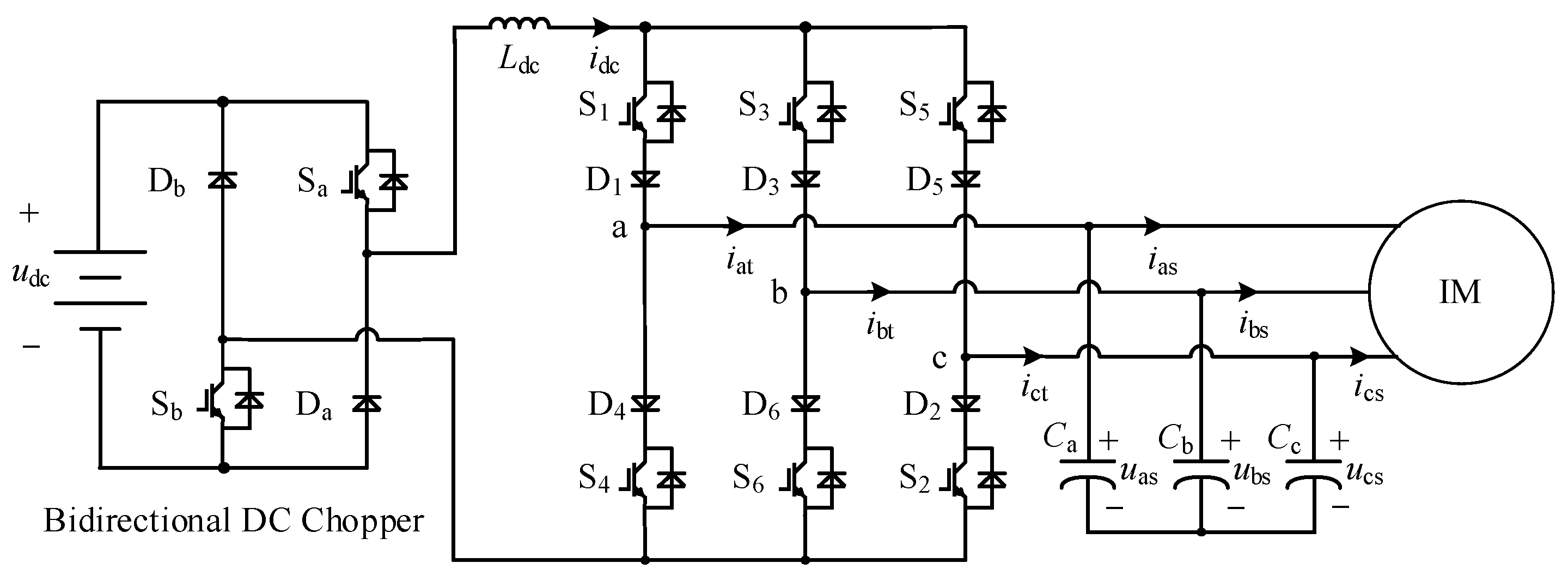
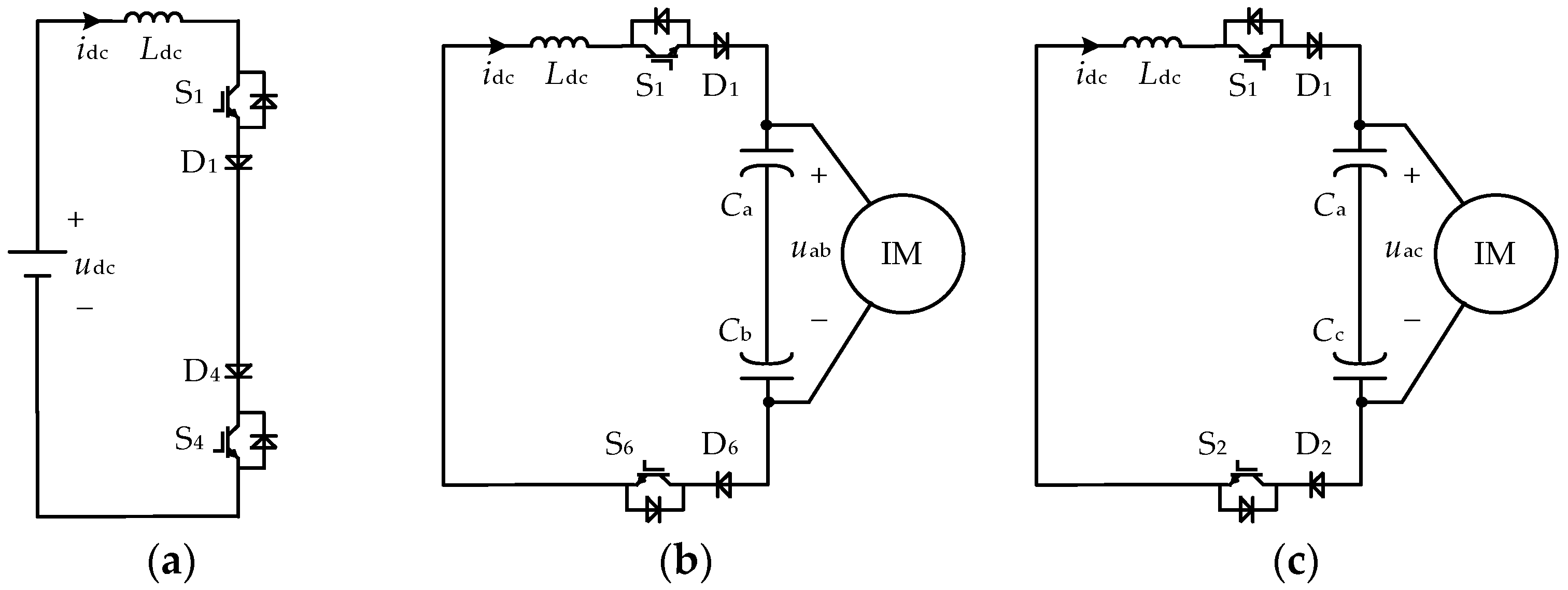
2.1. Topology of CSI-Fed IM Drive System with Bidirectional DC Chopper

To realize the decoupling control of the DC-link current and IM, a bidirectional DC chopper is added between the DC voltage source and DC-link inductor; the topology is shown in Figure 1. In the figure, udc is the DC input voltage; idc is the current of DC-link inductor Ldc; S1–S6 are six switching tubes of the inverter bridge; D1–D6 are the diodes connected in series with S1–S6; Ca, Cb and Cc are the three-phase filter capacitors in the AC side; iat, ibt and ict are the three-phase output currents of the inverter bridge; ias, ibs and ics are the stator currents of the IM; uas, ubs and ucs are the three-phase voltages of the filter capacitors. The bidirectional DC chopper is composed of the diodes Da, Db and the switching tubes Sa, Sb.
When the control method proposed in Ref. [17] is adopted, the circuit of DC input side can be regarded as a controlled current source. In the process of mathematical modeling and control system design for the AC side of CSI, the influence on the DC-link current can be ignored, and the topology of the CSI-fed IM drive system with bidirectional DC chopper can be simplified as seen in the circuit shown in Figure 2.

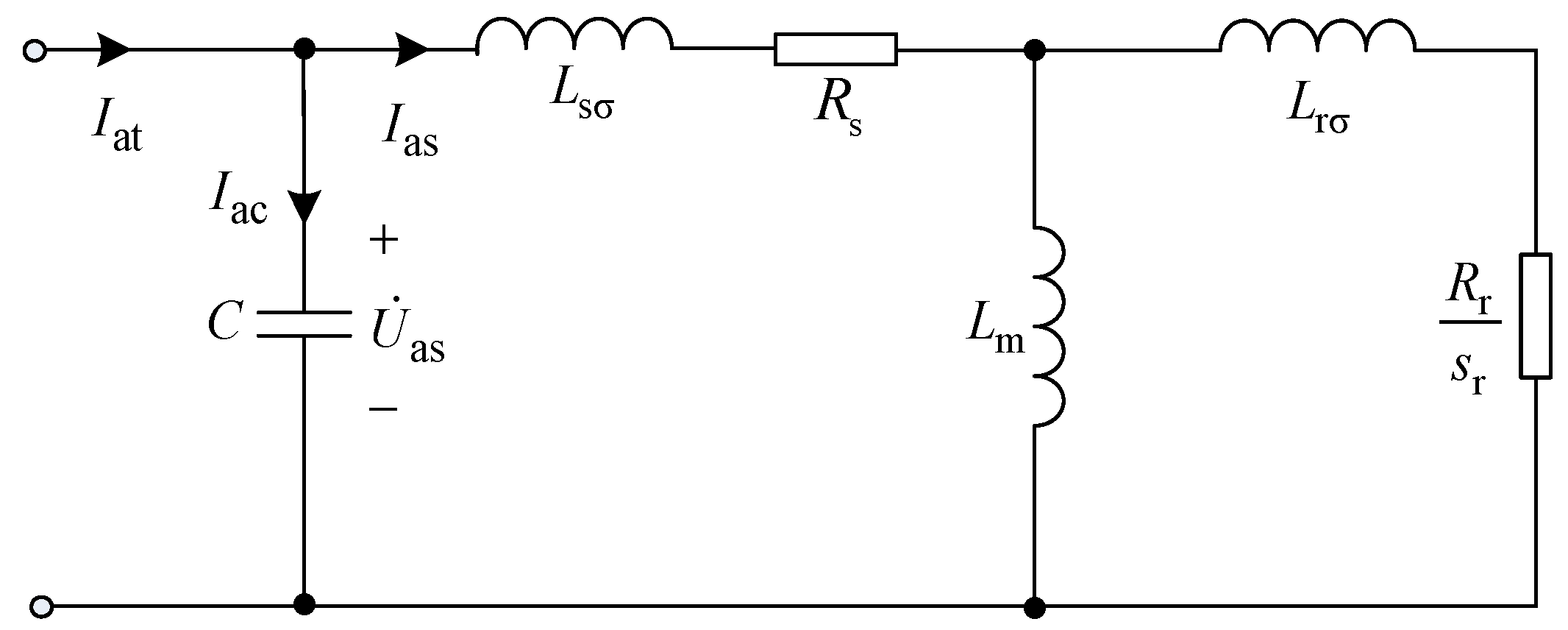
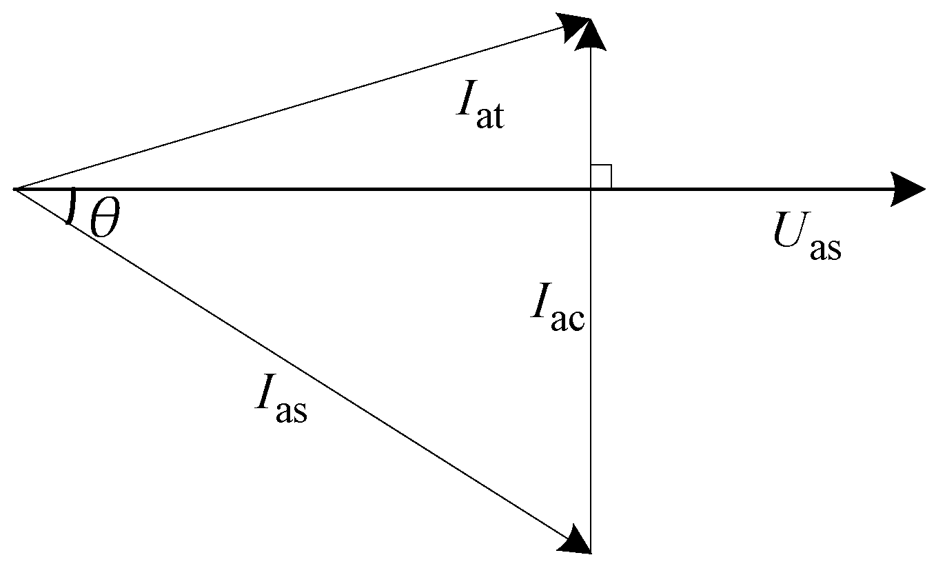
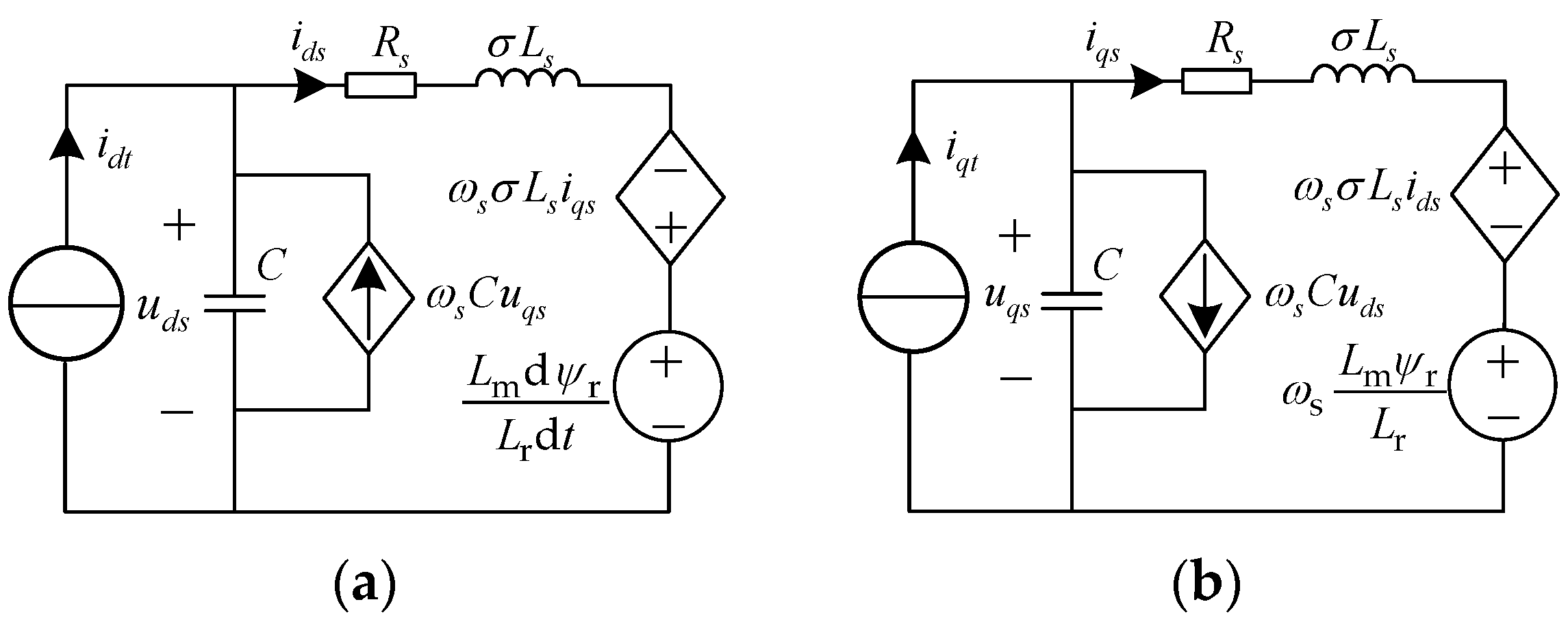
2.2. Mathematical Model of Filter Capacitors and IM

In the synchronous rotating frame (d-q axis) based on rotor flux orientation, the IM voltage equation can be expressed as
{ u ds = σ L s d i ds d t + i ds R s σ ω s L s i qs + L m d ψ r L r d t u qs = σ L s d i qs d t + i qs R s + σ ω s L s i ds + ω s L m ψ r L r
where ids and iqs are the stator currents in the d-q axis; uds and uqs are the voltages of filter capacitor in the d-q axis; ψr is the rotor flux; σ, Rs, Lm, Lr and ws are the flux leakage coefficient, stator resistor, mutual inductance, rotor inductance and synchronous angular frequency, respectively.
According to Figure 2, the current equation in three-phase stationary coordinate frame can be expressed as
{ C d u as d t = i at i as C d u bs d t = i bt i bs C d u cs d t = i ct i cs
where C represents the value of filter capacitors. Clarke transform and Park transform are carried out on Formula (3); in turn, the current equation in the d-q axis can be obtained and expressed as
{ C d u ds d t = i dt i ds + ω s C u qs C d u qs d t = i qt i qs ω s C u ds
where idt and iqt are the output current of the inverter bridge in the d-q axis. The rotor flux equation in the d-q axis is expressed as
T r d ψ r d t + ψ r = L m i ds
where ψr and Lm are the rotor flux and excitation inductor of IM, respectively, and Tr is the rotor time constant. The equations of torque and speed are expressed as
{ T e = n p L m L r ψ r i qs J d ω r d t = T e T L
where J is the moment of inertia, ωr is the mechanical speed, and Te and TL are the electromagnetic torque and load torque, respectively.
In summary, the mathematical model of filter capacitors and IM in the AC side of CSI can be represented by Equation (1) to Equation (5).

3. Parameter Design of DC-Link Inductance and AC-Filter Capacitance

3.1. Selection Range of DC-Link Inductance

A strong output impedance and constant current source characteristics of the DC side in CSI can be obtained by a larger DC-link inductance. However, the current regulation becomes slower as the inductance increases, which leads to overmodulation and generates low-order current harmonics. Therefore, it is necessary to determine a selection range of DC-link inductance.
In the start-up stage, the DC-link current is too low to provide the required current for the IM, so the zero switching state is adopted, and Ldc is charged by udc; the equivalent circuit is shown in Figure 3a. The state equation of idc is expressed as
L dc d i dc d t = u dc
where Tup_max is the maximum allowable charging time, making sure that the charging time for idc to increase from zero state to maximum DC-link current idc_max is less than Tup_max. Ldc should satisfy the following condition:
L dc < u dc T up _ max i dc _ max
According to the conclusion in Ref. [21], the current fluctuation ∆idc can be calculated when the IM is powered independently by Ldc, which contains two active switching states in one carried period. For example, in sector I, the equivalent discharge circuits are shown in Figure 3b,c, and ∆idc is expressed as
Δ i dc = 3 T s U I cos θ 2 L dc i dc
where Ts is the carried period, equal to 100 µs; U is the fundamental amplitude of the stator voltage; I is the fundamental amplitude of the stator current; θ is the phase deviation between stator voltage and stator current. In other sectors, the voltage of Ldc and the switching state are shown in Table 1, and the expression of ∆idc is consistent with that of sector I, as shown in Equation (8). Making sure that ∆idc is less than the maximum ripple ∆idc_max under θ = 1, Ldc should satisfy the follow condition:
L dc > 3 m imax m umax T s u dc 2 Δ i dc _ max
where mimax and mumax are the maximum modulation ratio and boost ratio of CSI, respectively. Combining Equations (7) and (9), the selection range of Ldc is expressed as
L dc ( 3 m imax m umax T s u dc 2 Δ i dc _ max , u dc T up _ max i dc _ max )
The parameters are set as follows: mimax = 1, mumax = 1, udc = 24 V, ∆idc_max = 1 A, idc_max = 50 A and Tup_max = 20 ms. Substituting the above parameters into Equation (10), the minimum value and maximum value of DC-bus inductance are 3.6 mH and 9.6 mH, respectively.

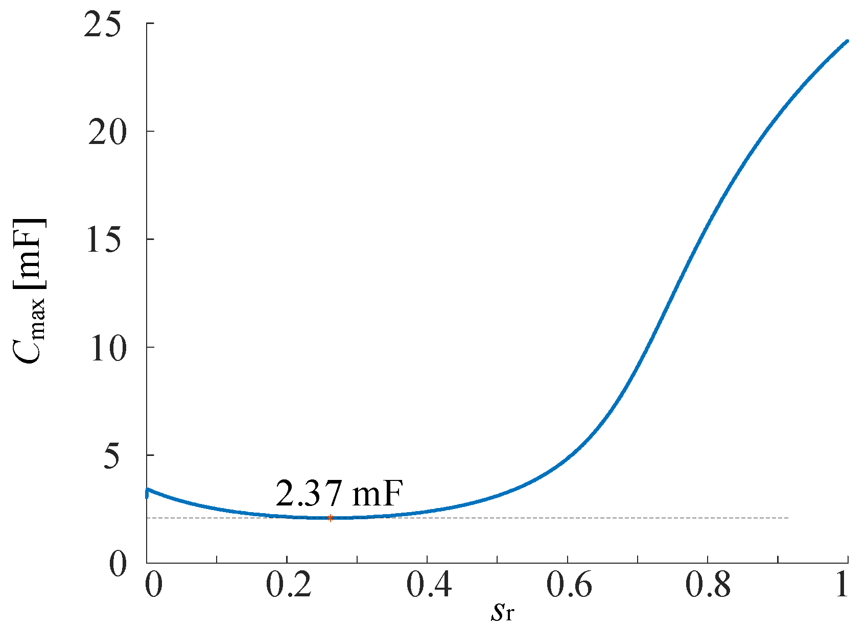
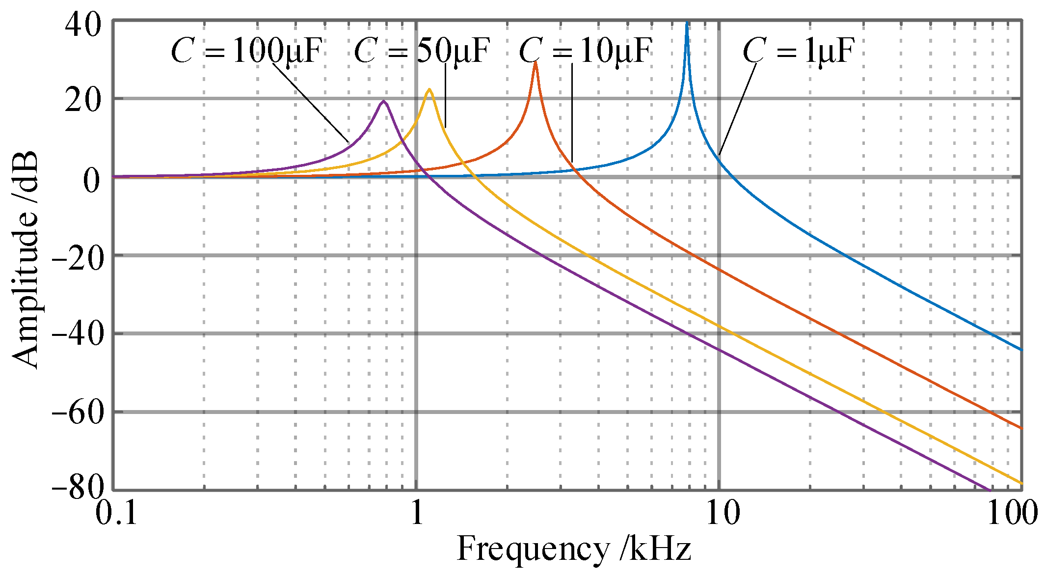
3.2. Selection Range of AC-Filter Capacitance

The IM is represented by the T-type equivalent circuit; the phase-a circuit model of IM and the capacitor is shown in Figure 4, where L and L are the stator leakage inductor and rotor leakage inductor, respectively; Rr is the rotor resistor; Iac is the current vector of Ca; and sr is the slip ratio.
The vector diagram composed of Iat, Ias, Iac and Uas is shown in Figure 5, and the following relationship can be obtained:
I at = I ac + I at = j ω s C U as + I as
In order to maximize the AC current utilization rate, the following equation should be satisfied:
I at     I as
According to the geometric relationship in Figure 5, Iac should be satisfied as follows:
I ac     I as sin θ
Substituting Equation (11) into Equation (13), the expression of maximum capacitance Cmax can be obtained as
C C max = 2 I as sin θ ω s U as
The mathematical relationship of Uas, Ias and sinθ can be obtained according to the T-type equivalent circuit of IM shown in Figure 4, and Equation (14) can be rewritten as
C C max = 2 ( ω s L s σ + A / B ) ω s ( R s + A / B ) 2 + ( ω s L s σ + D / B ) 2
where the specific forms of A, B and D are expressed as
{ A = ( R r R m s r ω s 2 σ L r L m ) ( R r s r + R m ) + ( R r ω s L m s r + R m ω s σ L r ) ( ω s σ L r + ω s L m ) B = ( R r s r + R m ) 2 + ( ω s σ L r + ω s L m ) 2 D = ( R r ω s L m s r + R m ω s σ L r ) ( R r s r + R m ) ( R r R m s r ω s 2 σ L r L m ) ( ω s σ L r + ω s L m )
From Equations (15) and (16), Cmax is a function of sr, and ωs is set as the rated angular frequency of 100π rad/s. Substituting the IM parameters listed in Table 2 into Equations (14) and (15), the relationship curve between Cmax and sr can be obtained, which is shown in Figure 6. It is obvious that a minimum value occurs in Cmax, so the AC-filter capacitance should be less than 2.37 mF.
Next, the influence mechanism on harmonic characteristics of the stator current caused by AC-filter capacitance will be discussed. The T-type equivalent circuit of IM is a third-order system; it is difficult to derive the transfer function and mathematical relationship between the capacitance and bandwidth. Since the high-order harmonic contents near the switching frequency of ids (iqs) are same as the stator currents in three-phase stationary coordinate, according to Equations (1) and (2), the equivalent circuits of the IM and AC-filter capacitor in the d-q axis based on rotor flux orientation are established, as shown in Figure 7. idt and iqt are composed of a DC component and several high-order harmonics components near the switching frequency. The equivalent controlled current sources, voltage sources, and back EMFs in Figure 7 cannot amplify or attenuate harmonics, so the suppression effect of high-order harmonics is determined by Rs, σLs and C, and the transfer function Git2is(s) from idt (iqt) to ids (iqs) can be expressed as
G it 2 is ( s ) = 1 σ L s C s 2 + R s C s + 1
and the oscillation angular frequency ωn can be expressed as
ω n = 1 σ L s C
Substituting the value of Rs and Ls into Equation (16), the Bode plot of Git2is(s) is drawn under different AC-filter capacitance, which is shown in Figure 8. It can be seen that Git2is(s) has a resonance spike, and the cutoff frequency decreases with the increase of C. In order to obtain the high quality stator current, Git2is(s) should effectively suppress the harmonic components in iat near the switching frequency fs, so the oscillation frequency should be far below fs. This paper stipulates that the oscillation frequency is less than fs/2; according to Equation (17), AC-filter capacitance should be satisfied as
C > 1 σ L s π 2 f s 2
Substituting the IM parameters listed in Table 2 into Equation (19), the minimum value of C is 2.5 µF.

4. Design Principle for Vector Control Strategy of CSI-Fed IM Drive System

According to Section 1, the mathematical model formed by the IM and capacitor is a third-order system; when the three closed-loop control strategy is adopted, more voltage sensors are needed, and the dynamic response to torque is slower than the VSI-fed IM drive system. In this section, a novel vector control strategy without a voltage inner loop for the CSI-fed IM drive system will be proposed, which includes current loop, flux loop and speed loop.

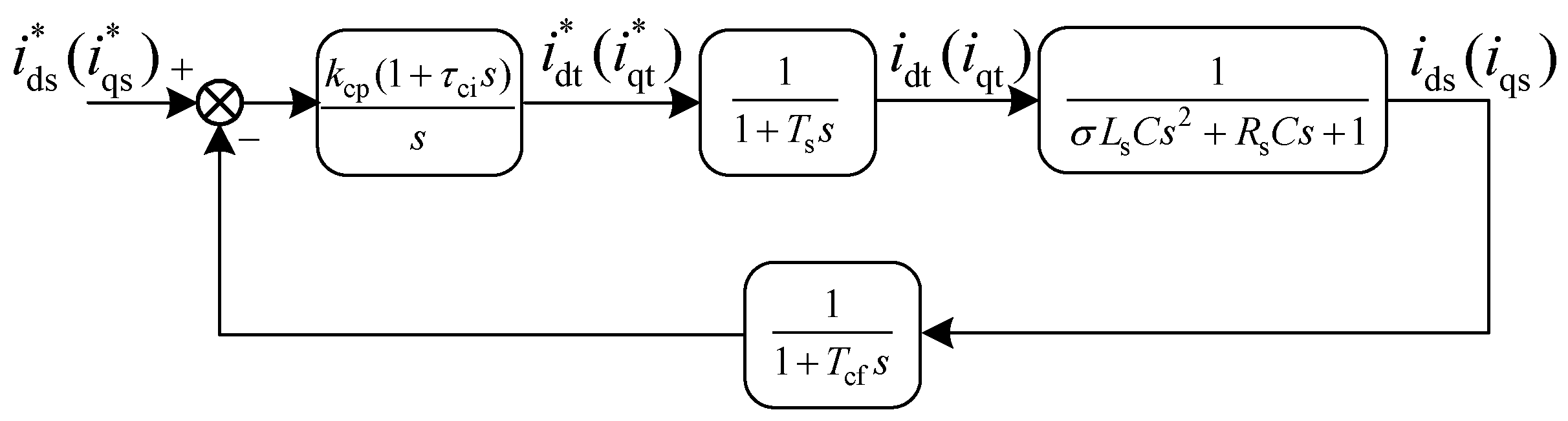
4.1. Analysis and Parameter Design for Current Loop

The switching delay and digital control delay are equivalent to a first-order transfer function, which is expressed as
G d ( s ) = 1 1 + T s s
Due to the presence of high-frequency noise in the stator current sampling signal, a filter circuit is adopted in this paper, and its equivalent transfer function is
G cf ( s ) = 1 1 + T cf s
where Tcf is the filter time constant, equal to 6 × 10⁻⁵ in this paper.
Ignoring the coupling terms in Equations (1) and (3), such as ωsσLsiqs, ωsσLsids, ωsCuqs and ωsCuds, in the d-q axis, the control diagram of the current loop without stator voltage sampling and control is shown in Figure 9, where kcp and τ ci are the proportional coefficient and integral coefficient of PI controller for adjusting the stator current, i dt * and i qt * are the reference value of output current of the inverter bridge in the d-q axis, i ds * and i qs * are the reference value of the stator currents in the d-q axis.
In this paper, the target cut-off frequency and phase margin of current loop are represented as ωcc and φcc. According to Figure 9, Qc_amp, the amplitude of the current open-loop at ωcc, can be derived as follows:
Q c _ amp = 1 [ 1 + ( T s ω cc ) 2 ] [ 1 + ( T cf ω cc ) 2 ] [ ( 1 σ L s C ω cc 2 ) 2 + R s 2 C 2 ω cc 2 ]
φc_phase, the phase of the current open-loop at ωcc, can be derived as follows:
φ c _ phase = arctan ( T s ω cc ) arctan ( T cf ω cc ) arctan ( R s C ω cc 1 σ L s C ω cc 2 )
To ensure that the phase angle margin of the current loop with the PI controller is greater than φcc, τ ci should be satisfied as follows:
τ ci tan ( φ cc φ c _ phase π 2 ) ω cc
To ensure that the amplitude of the current loop with the PI controller is equal to 1, kcp should be satisfied as follows:
k cp = ω cc Q c _ amp 1 + τ ci 2 ω cc 2
In order to achieve fast dynamic response and the effective suppression of high-order harmonics in the output current of the inverter bridge, ωcc is set to 2000π rad/s, which is one-tenth of the switching frequency. Meanwhile, to obtain a better stability, φcc is set to π/4 rad. Substituting the parameters listed in Table 2 into Equation (22) to Equation (25), kcp and τ ci can be calculated as 0.98 and 22.15, respectively. The Bode plot of the current closed-loop transfer function Gi(s) is shown in Figure 10; the bandwidth of Gi(s) is 1kHz, and the amplitude remains 0 dB when the frequency is less than 1kHz. When the frequency is greater than 1 kHz, the amplitude decays with a slope close to −60 dB/dec, which can effectively suppress the high-order harmonics generated in the switching process. This explains that a good steady-state and dynamic performance can be achieved by the PI parameter optimization proposed in this paper. In order to facilitate the subsequent parameter design of the external loop control system, Gi(s) is simplified to a second-order transfer function and expressed as
G i ( s ) = 3.13 × 10 5 1.65 × 10 3 s 2 + 37.1 s + 3.13 × 10 5

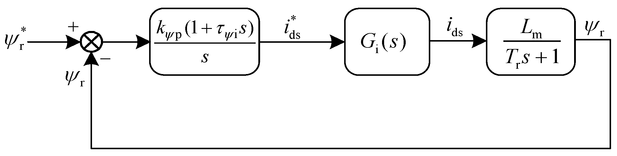
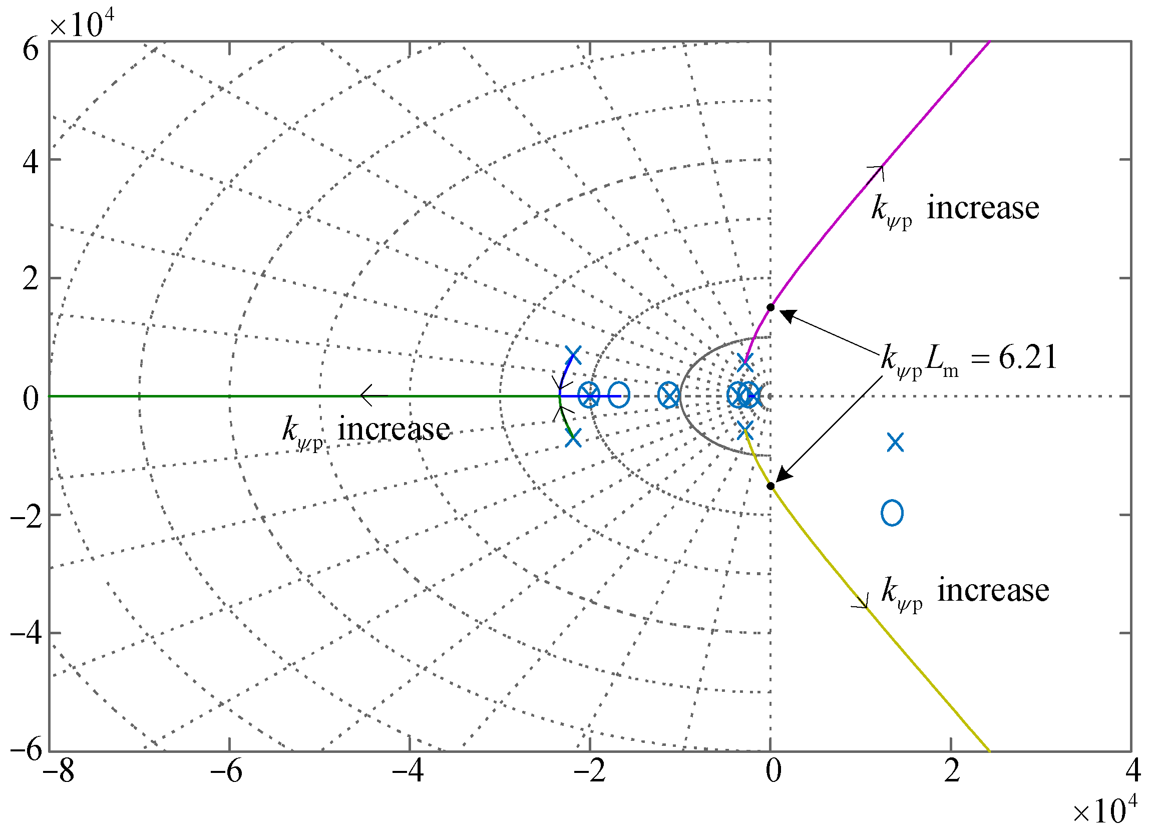
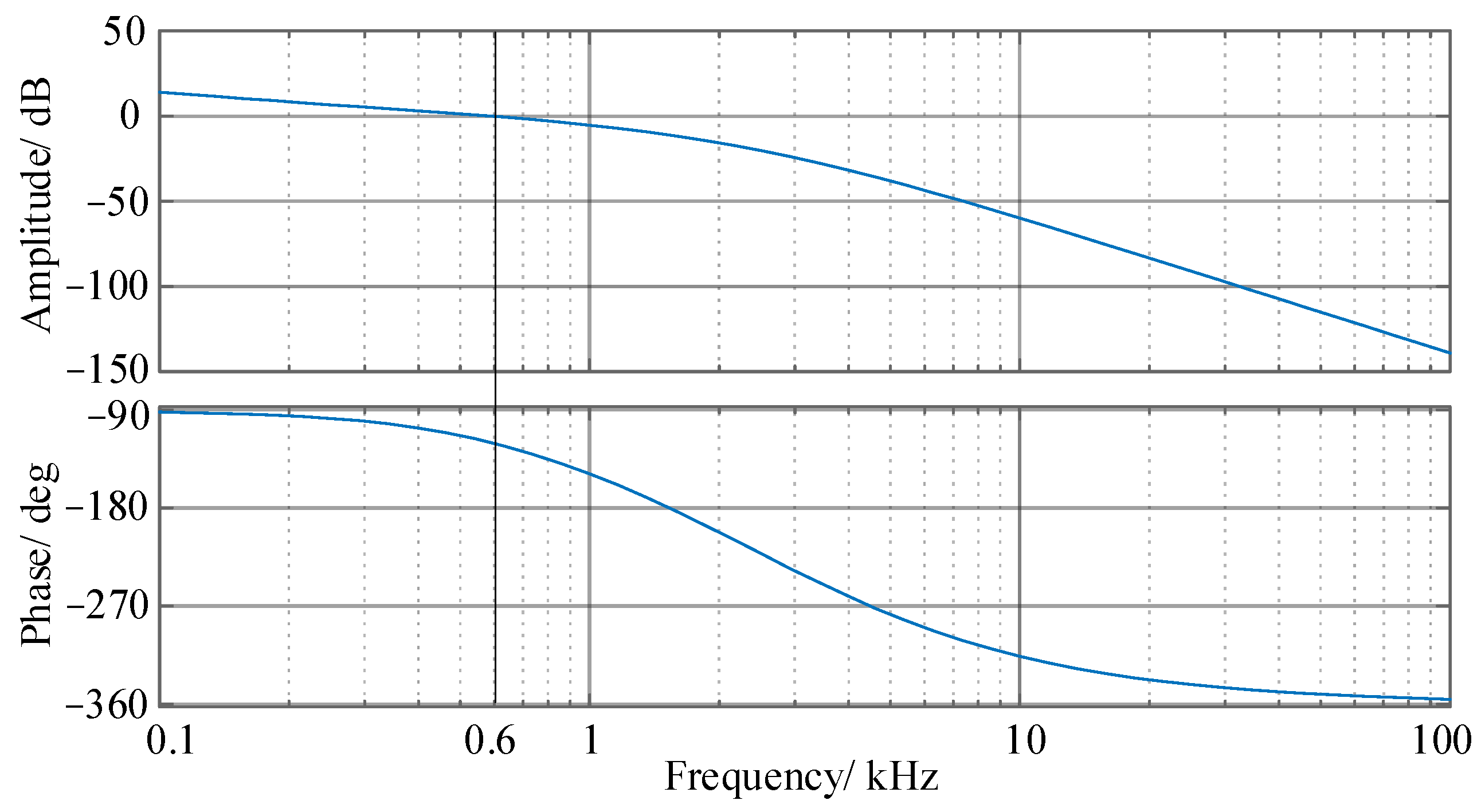
4.2. Analysis and Parameter Design for Flux Loop

A PI controller is adopted to adjust rotor flux ψr and is combined with Equation (4); the diagram of the flux loop with a PI controller is shown in Figure 11. kψp and τ ψ i are the proportional coefficient and integral coefficient of the PI controller.
To simplify the design method of the control parameters, zero-pole cancellation is adopted, and τ ψ i is set to Tr. Then, the root locus plot is utilized to determine kψp, which is shown in Figure 12. It is obvious that the condition for the stability of the flux loop is as follows:
k ψ P ( 0 , 6.21 / L m )
Finally, kψp is obtained by the Sisotool box of Matlab, where kψp is equal to 3.15/Lm; the Bode plot of flux open-loop is shown in Figure 13. The cut-off frequency is 600 Hz, and the phase margin is 60°.

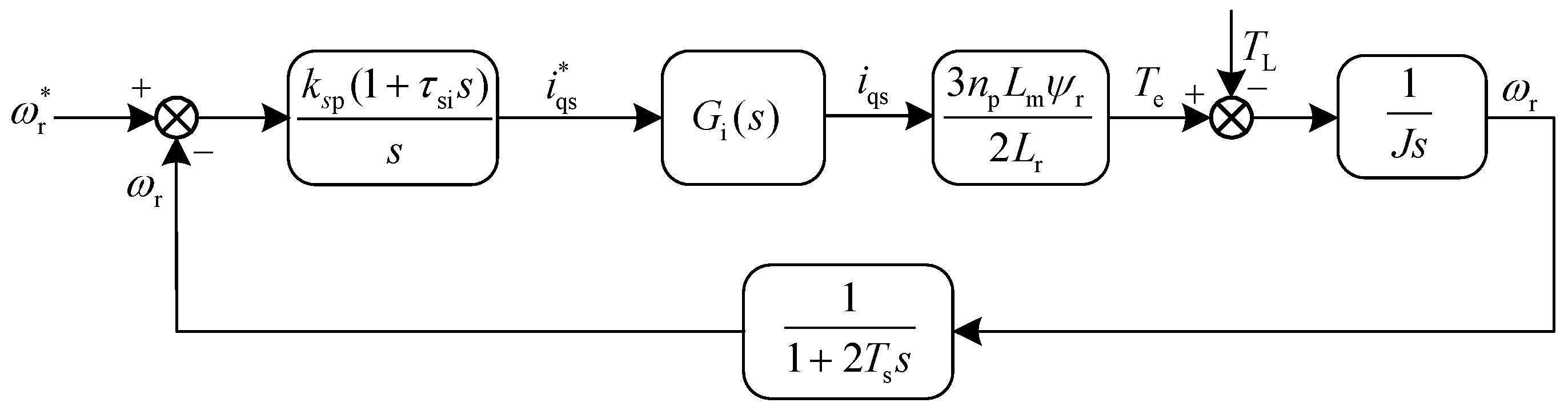
4.3. Analysis and Parameter Design for Speed Loop

The speed of IM is sampled by an orthogonal encoder, and the sampling frequency is half of fs; the transfer function of speed sampling and delay is expressed as
G sf ( s ) = 1 1 + 2 T s s
In accordance with Equations (5) and (6), the block diagram of the speed loop under the PI controller is shown in Figure 14, where ksp and τ si are the proportional coefficient and integral coefficient of the PI controller for adjusting the stator current, respectively. ω s * is the rated angular frequency. It is noted that the speed loop contains variable ψr, so the cut-off frequency of the speed open loop should be less than that of the flux open loop, and ψr is set as 0.05 Wb. The open-loop transfer function of speed Gs_open(s) can be expressed as
G s _ open ( s ) = 3 n p L m ψ r k sp G i ( s ) ( 1 + τ si ) 2 J L r s 2 ( 1 + 2 T s s )
The close-loop transfer function of speed Gs_close(s) is expressed as
G s _ close ( s ) = G s _ open ( s ) ( 1 + 2 T s s ) 1 + G s _ open ( s )
The target cut-off frequency and phase margin of the speed loop are represented as ωss and φss. Using the same method as the current PI controller, the analytical formulas of ωss and φss are derived as follows:
{ τ si = tan ( φ ss φ s _ phase π 2 ) ω ss k sp = ω ss Q s _ amp 1 + τ si 2 ω ss 2
where Qs_amp and φs_phase are the amplitude and phase of the speed open loop at ωss before the PI controller, respectively. ksp and τ si are obtained by substituting the equation ωss = 200π rad/s and φss = π/6 rad into Equation (31). The specific expression of Gs_close(s) is as follows:
G s _ close ( s ) = 30.89 s 4 + 8.5 × 10 5 s 3 + 9.34 × 10 9 s 2 + 2.93 × 10 13 s + 2.93 × 10 11 5.425 × 10 10 s 7 + 2.716 × 10 5 s 6 + 0.6 s 5 + 7045 s 4 + 4.29 × 10 7 s 3 + 1.01 × 10 11 s 2 + 2.93 × 10 13 s + 2.93 × 10 11
The Bode plots of open-loop and closed-loop transfer functions are shown in Figure 15. The cut-off frequency of the speed open-loop transfer function is 100 Hz, and the phase margin is 30°. The closed-loop transfer function has a good following characteristic in the bandwidth of 40 Hz. The unit step response of the speed closed-loop transfer function is shown in Figure 16; the rise time is only 2 ms, the overshoot is little, and no steady-state error occurs.

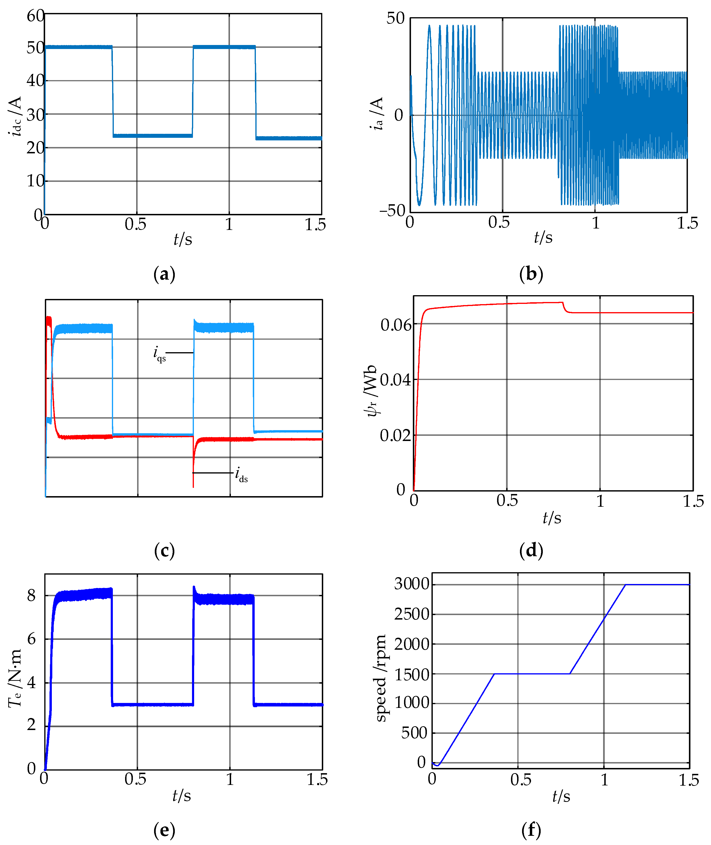
5. Simulation Results

The simulation model of the CSI-fed IM drive system with bidirectional DC chopper is built on MATLAB Simulink, including the power module, control module and modulation module. The parameters of IM adopted are consistent with Table 2, and other simulation parameters are shown in Table 3.

5.1. Load Acceleration Condition

The value of load torque is set to 3 N·m, the initial reference speed is 1500 rpm, and the reference speed is 3000 rpm when the time is 0.8 s. The simulation waveforms of stator phase a current, stator currents in the d-q axis, electromagnetic torque, motor speed and rotor flux in the whole simulation process are shown in Figure 17.
To improve DC-link current utilization and reduce losses and harmonic distortion, according to the MTPA method proposed in Ref. [17], the references of rotor flux and DC-link current are adjusted with the change of operating point; the specific principle is as follows:
A.
In the dynamic process, in order to provide greater torque, the reference DC-link current is set to 50 A, which is the maximum current of the DC-link inductor.
B.
In the steady state, the references of rotor flux ψ r * and DC-link current i dc   * are adjusted according to the load torque and speed, which are shown in Table 4.
The whole simulation process is divided into three stages.
Start-up stage: in order to make the motor speed reach the reference speed as soon as possible, the hysteresis control strategy of DC-link current is adopted to regulate idc to 50 A, which is the max reference, so as to meet the demand of current. The optimal reference value of rotor flux ψ r * is 0.068 Wb. After 0.05 s, ψ r * reaches the reference value, ids is around 15 A, iqs is around 43 A, and Te is 8 N·m. After 0.4 s, the speed is adjusted to 1500 rpm, and Te is reduced to 3 N·m.
Steady-state operation stage at 1500 rpm: idc is regulated to 23.5 A, as shown in Figure 17a. It can be seen from Figure 17e that when idc is reduced to 23.5 A, the ripple of torque is significantly reduced.
Second acceleration stage: at the time of 0.8 s, the value of step speed is 3000 rpm. idc reach to 50 A again, which is the same as the start-up stage. When ψ r * is adjusted to 0.064 Wb, ids is reduced immediately, ψ r follows the given value quickly, iqs and Te are the same as the start-up. Finally, at 1.08 s, the speed reaches to 3000 rpm.

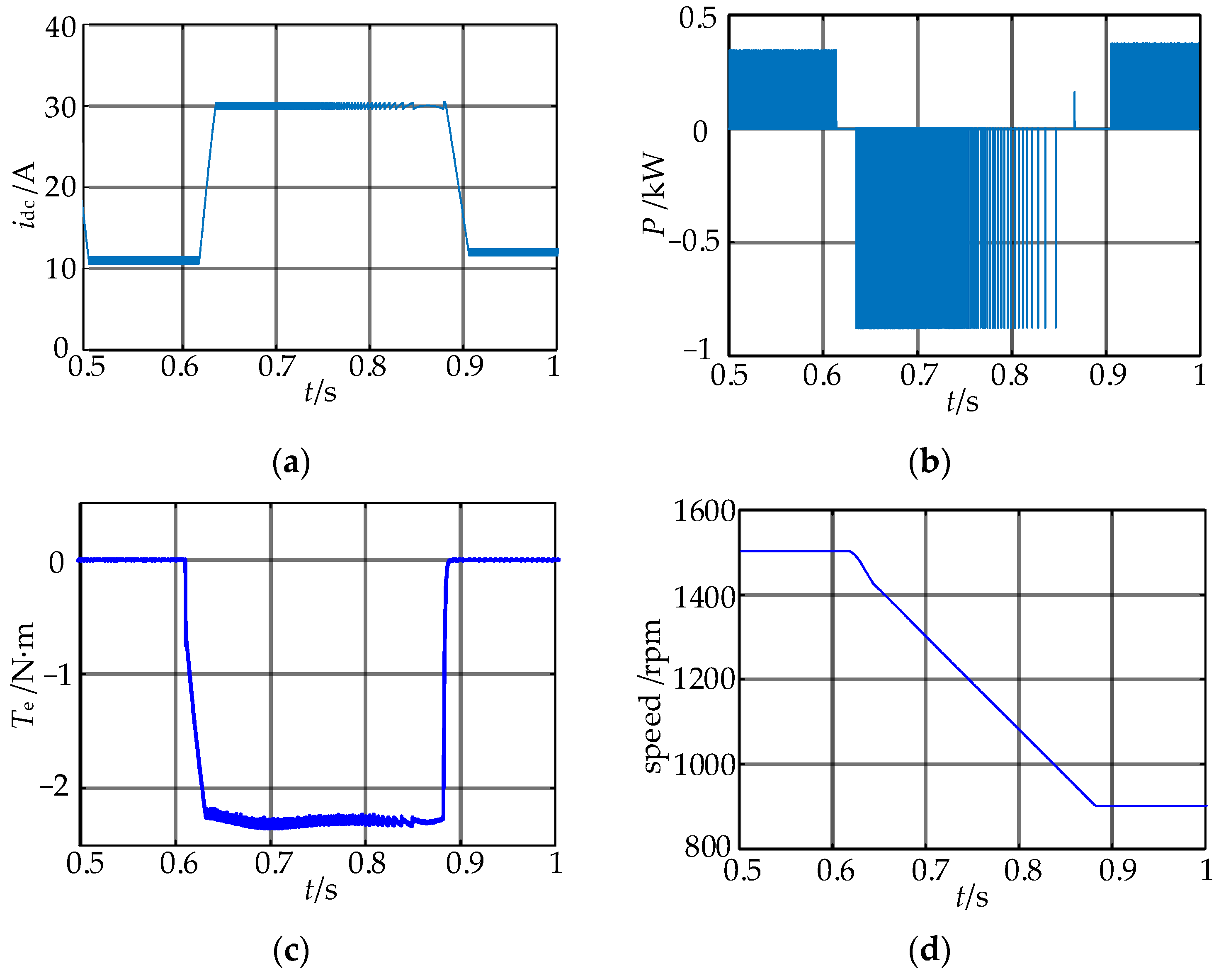
5.2. Deceleration Condition with No Load

This section simulates the deceleration condition of the motor with no load. When the IM speed reaches the rated speed of 1500 rpm, the reference speed is changed to 900 rpm at 0.6 s. The simulation waveforms of electromagnetic torque, speed, DC-link current and output power of DC power supply are shown in Figure 18, respectively. When the speed decelerates, idc is around 30 A. The electromagnetic torque plays a braking role and reaches to −2.3 N·m, and the speed reaches stability again after 0.28 s. The DC power supply intermittently absorbs the energy feedback from the motor decelerating process, and the output power is less than zero, so the energy feedback is realized.

5.3. Load Disturbance Condition

Figure 19 are the simulation waveforms of load disturbance, when the speed remains at 1500 rpm, the load torque is reduced from 3 N·m to 1 N·m at 0.1 s, and the speed controller makes the electromagnetic torque drop rapidly to 1 N·m, where the speed remains unchanged. At the same time, the ψr and idc are reduced to the optimal value of 0.039 Wb and the minimum value of 14.8 A, respectively. When the load torque is increased to 2 N·m at 0.3 s, the speed is stabilized at 1500 rpm after 0.16 s, and the maximum error of speed is only 14 rpm. The ψr and idc are adjusted to 0.055 Wb and 20.9 A, respectively.

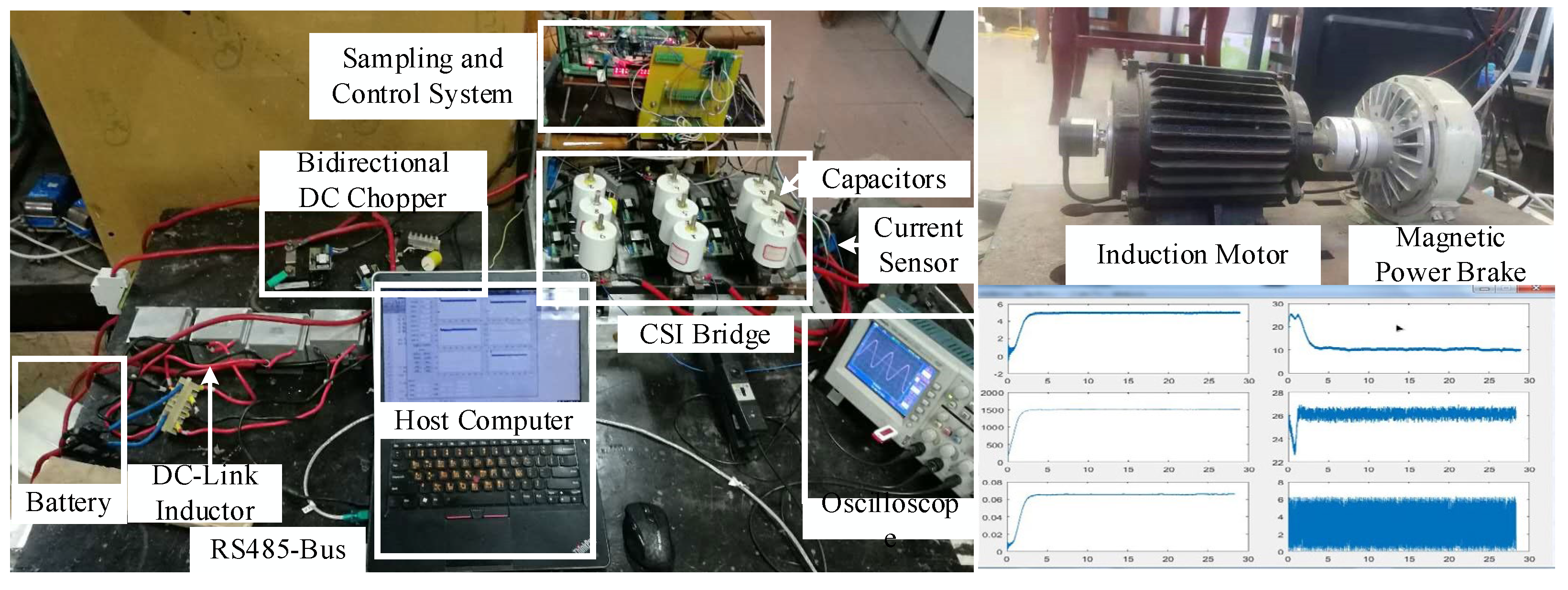
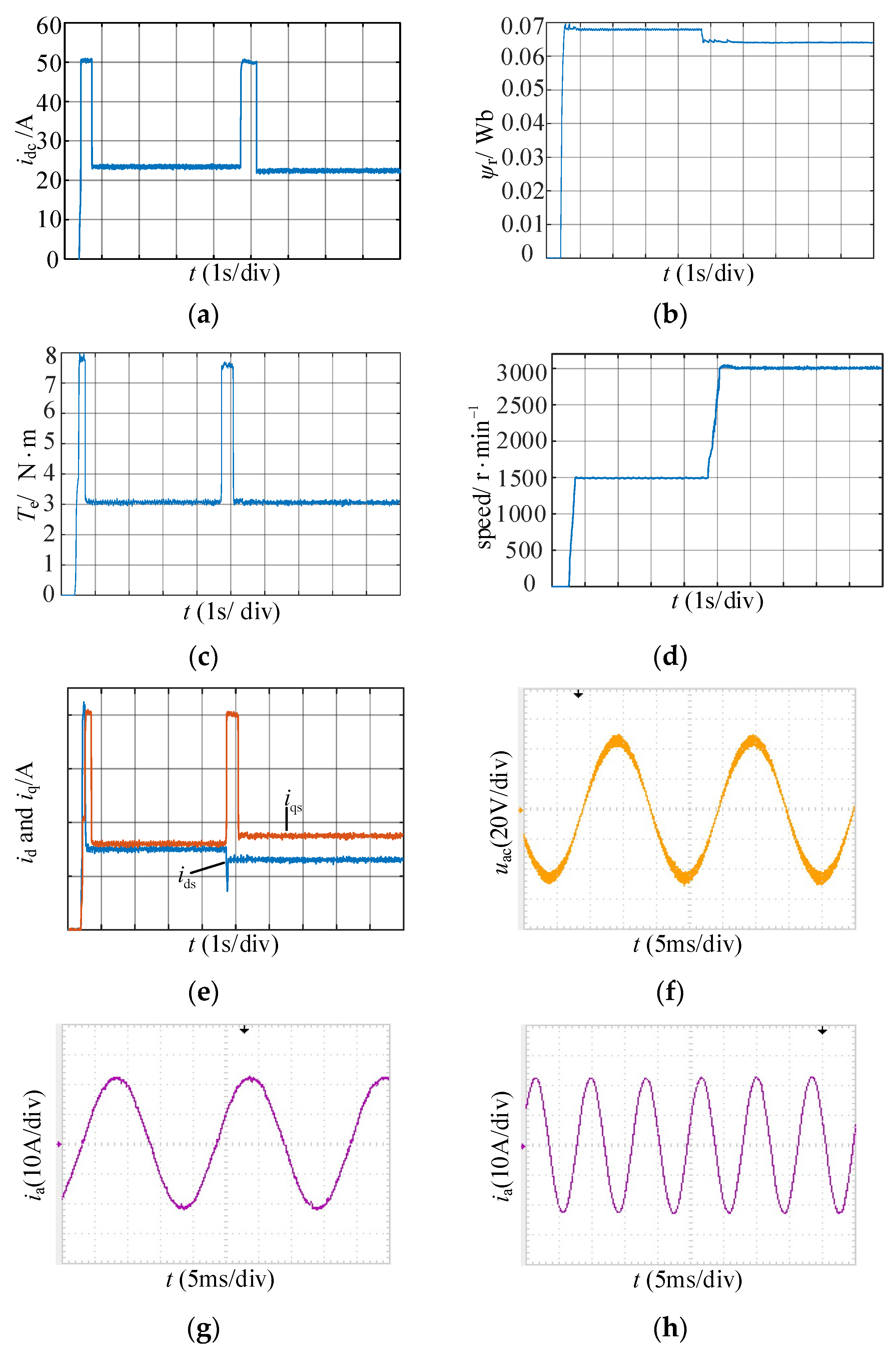
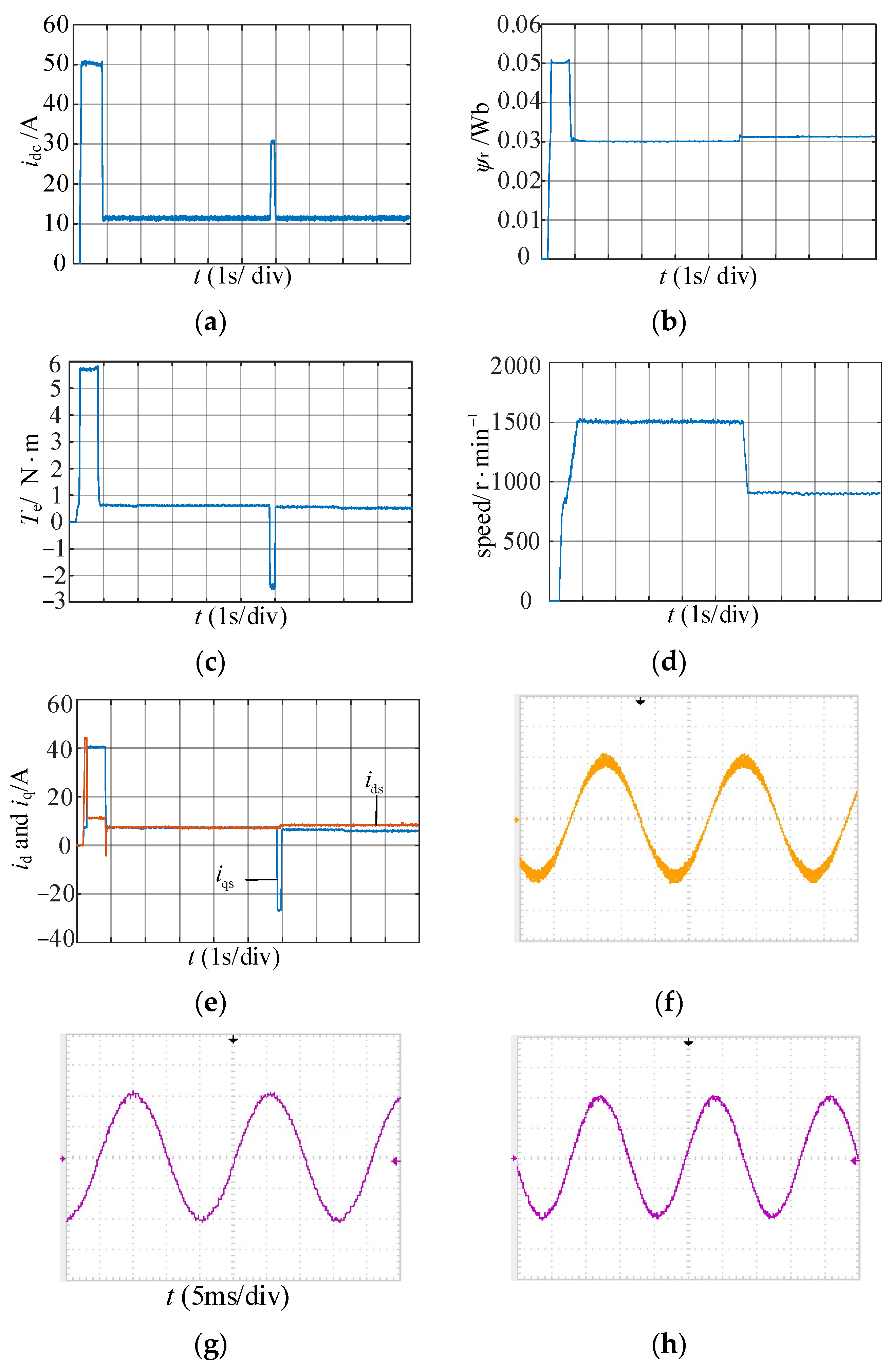
6. Experimental Results

In order to verify the feasibility of parameter design for DC-link inductance and AC-filter capacitance and the effectiveness of the vector control strategy proposed in this paper, the experimental platform was established, as shown in Figure 20; the experimental parameters are shown in Table 5. The value of DC-link inductance and AC-filter capacitance are satisfied with the selection range specified in Section 3. Because the motor speed, rotor flux, and stator d-q axis current cannot be measured by the oscilloscope, in order to facilitate debugging as well as the observation and storage of these signals, this paper develops a host computer program on the GUI platform of MATLAB to realize the data communication with DSP.
Next, the experimental results will be carried out under the three operation conditions: acceleration with load, deceleration with no-load and change of load.

6.1. Performance under Acceleration with Load of 3 N·m

Experimental waveforms of accelerated conditions are shown in Figure 21, under the load of 3 N·m. The experimental process consists of two stages. The reference speed changes from 1500 rpm to 3000 rpm, in order to reduce the harmonics and losses, and to improve current utilization, the references of idc and ψr are also adjusted according to the calculation method for the minimum DC-link current and the optimal flux proposed in Ref. [17]. In the dynamic process, to obtain a larger torque and reduce the dynamic response time, the reference idc is set to 50 A. In the first stage, the reference speed is set to 1500 rpm, and the reference idc and ψr are set to 23.5 A and 0.068 Wb, respectively. In the second stage, the reference speed is set to 3000 rpm, and the reference idc and ψr are set to 22.5 A and 0.065 Wb, respectively. From Figure 21, the rise time of idc increasing from 0 A to 50 A is only 15 ms, and the ripple of idc is less than 0.5 A, which demonstrates that the parameter design method of the DC-link inductor is feasible. In two stages, the speed and rotor flux can quickly track the references, and the THD of the stator current is less than 2%.

6.2. Performance under Deceleration with No Load

The experimental waveforms of the reference speed decreasing from 1500 rpm to 900 rpm with no load are shown in Figure 22. Unlike with the operational condition where the load is 3 N·m, the amplitude of the stator voltage is 18.5 V, which is less than udc. idc remains at 12 A with little ripple in the steady state, and during the dynamic process of speed decreasing from 1500 rpm to 900 rpm, the reference of idc is set to 30 A, and the mechanical energy from IM is recovered by the DC voltage source. Due to a fast dynamic and little ripple of Te, dynamic and steady performance of speed can be obtained, the rotor flux can quickly track the references, and the stator current has very little harmonic distortion.

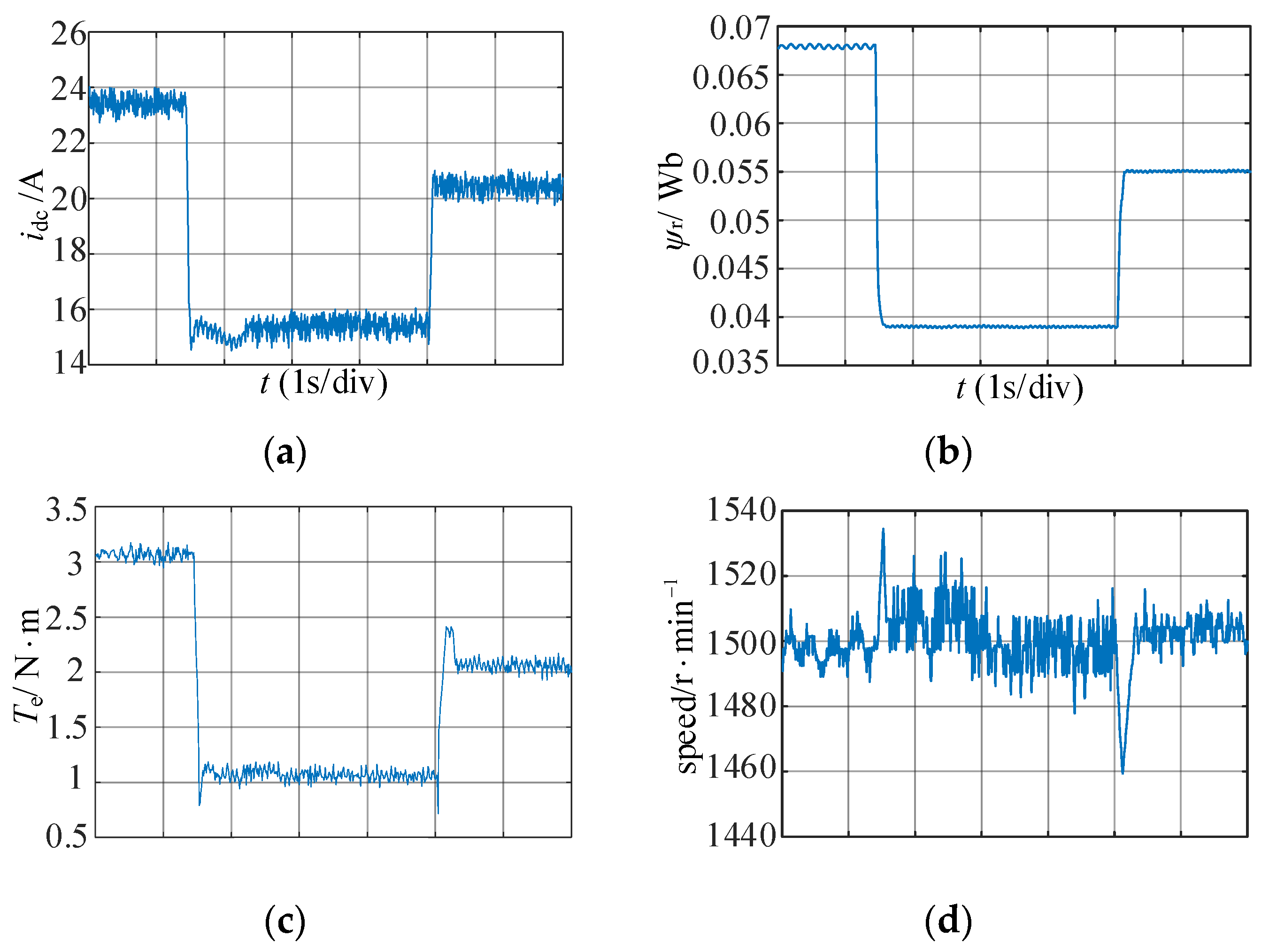
6.3. Performance under Different Loads

The reference speed is set to 1500 rpm. The IM starts with the load of 3 N·m, then the load is suddenly reduced to 1 N·m, and finally the load is increased to 2 N·m. The experimental waveforms are shown for the reference speed decreasing from 1500 rpm to 900 rpm with no load are shown in Figure 23. Since the torque can be quickly adjusted when the sudden change occurs on the load, the fluctuation of the speed is less than 3%. Meanwhile, idc and ψr can quickly track the references.

7. Conclusions

In order to improve the performance of the current source inverter–fed inductor motor drive system, this paper presents a novel design principle of DC-bus inductance and AC-filter capacitance, and a vector control technology without voltage loop. The feasibility and correctness are verified by the simulation and experimental results under various operating conditions. The main contributions can be summarized as follows:
(1)
Under consideration of the dynamic response speed and current ripple, the range expression of the DC-link inductance is derived.
(2)
Under consideration of the DC-link current utilization and harmonic suppression, the range expression of the AC-filter inductance is derived.
(3)
The simulation and experimental results show that the fast dynamic performance of speed and flux with no overshoot and a stator current with low harmonic distortion can be obtained by the vector control strategy without voltage loop for current source inverter–fed inductor motor drive systems. The analytical expressions of the control parameters derived in this paper are also suitable for other IM parameters.

Author Contributions

Conceptualization and methodology, P.S.; simulation, Y.L.; validation and experiment, P.S. and C.L.; writing and supervision, P.S.; review and editing, C.L. funding acquisition, P.S. All authors have read and agreed to the published version of the manuscript.

Funding

This work was supported in part by the Southwest Petroleum University City-School Cooperation Strategic Project under Grant 18SXHZ0043.

Data Availability Statement

Not applicable.

Conflicts of Interest

The authors declare that there is no conflict of interest regarding the publication of this paper.

References

  1. Lorenzani, E.; Migliazza, G.; Immovilli, F.; Buticchi, G. CSI and CSI7 current source inverters for modular transformerless PV inverters. Chin. J. Electr. Eng. 2019, 5, 32–42. [Google Scholar] [CrossRef]
  2. Wang, W.; Gao, F.; Yang, Y. An eight-switch five-level current source inverter. IEEE Trans. Power Electron. 2018, 34, 8389–8404. [Google Scholar] [CrossRef] [Green Version]
  3. Zhou, S.; Liu, K.; Hu, W.; Chen, Y.; Zhang, D.; Huang, Q.; Tong, Q.; Zhang, Q. Harmonic-Separation-Based Direct Extraction and Compensation of Inverter Nonlinearity for State Observation Control of PMSM. IEEE Access 2021, 9, 142028–142045. [Google Scholar] [CrossRef]
  4. Dong, Z.; Liu, C.; Song, Z.; Liu, S. Suppression of Dual-Harmonic Components for Five-Phase Series-Winding PMSM. IEEE Trans. Transp. Electrif. 2022, 8, 121–134. [Google Scholar] [CrossRef]
  5. Zhao, L.; Chen, Z.; Wang, H.; Li, L.; Mao, X.; Li, Z.; Zhang, J.; Wu, D. An Improved Deadbeat Current Controller of PMSM Based on Bilinear Discretization. Machines 2022, 10, 79. [Google Scholar] [CrossRef]
  6. Zhao, J.; Lu, H. Study on a new control strategy based on three phase current inverter. In Proceedings of the 2017 Eighth International Conference on Intelligent Control and Information Processing (ICICIP), Hangzhou, China, 3–5 November 2017; pp. 151–156. [Google Scholar]
  7. Rajeev, M.; Agarwal, V. Single phase current source inverter with multiloop control for transformerless grid—PV interface. IEEE Trans. Ind. Appl. 2018, 54, 2416–2424. [Google Scholar] [CrossRef]
  8. Chen, D.; Jiang, J.; Qiu, Y.; Zhang, J.; Huang, F. Single-stage three-phase current-source photovoltaic grid-connected inverter high voltage transmission ratio. IEEE Trans. Power Electron. 2016, 32, 7591–7601. [Google Scholar] [CrossRef]
  9. Xing, L.; Wei, Q. Series-connected current source inverters with less switches. IEEE Trans. Power Electron. 2019, 35, 5553–5556. [Google Scholar] [CrossRef]
  10. Xu, Y.; Wang, Z.; Liu, P.; Wu, J.; Cheng, M. A new control method for current-source inverter fed motor drive system without additional DC-link current regulator. In Proceedings of the 2020 IEEE 9th International Power Electronics and Motion Control Conference (IPEMC2020-ECCE Asia), Nanjing, China, 29 November–2 December 2020; pp. 382–387. [Google Scholar]
  11. Miao, Y.; Liu, H.; Wang, H.; Wang, M. The modulation and control strategy of storage inductance current for single-phase current source inverter. Trans. China Electrotech. Soc. 2018, 33, 1227–1237. [Google Scholar]
  12. Wang, W.; Gao, F.; Yang, Y.; Blaabjerg, F. Operation and modulation of H7 current-source inverter with hybrid SiC and Si semiconductor switches. IEEE J. Emerg. Sel. Top. Power Electron. 2017, 6, 387–399. [Google Scholar] [CrossRef]
  13. Li, Y.W.; Pande, M.; Zargari, N.R.; Wu, B. DC-link current minimization for high-power current-source motor drives. IEEE Trans. Power Electron. 2008, 24, 232–240. [Google Scholar]
  14. Ding, L.; Li, Y.W.; Zargari, N.R. Discrete-time SMO sensorless control of current source converter-fed PMSM drives with low switching frequency. IEEE Trans. Ind. Electron. 2020, 68, 2120–2129. [Google Scholar] [CrossRef]
  15. Yang, S.; Peng, F.Z.; Lei, Q.; Inoshita, R.; Qian, Z. Current-fed quasi-Z-source inverter with voltage Buck–Boost and regeneration capability. IEEE Trans. Ind. Appl. 2010, 47, 882–892. [Google Scholar] [CrossRef]
  16. Xu, Y.; Wang, Z.; Liu, P.; He, J. A Soft-Switching Current-Source-Inverter-Fed Motor Drive With Reduced Common-Mode Voltage. IEEE Trans. Ind. Electron. 2021, 68, 3012–3021. [Google Scholar] [CrossRef]
  17. Miao, Y.; Liu, H.; Zhang, W.; Liu, P. Optimal control strategy of storage inductor current and rotor flux for current source inverter motor drive system. Proc. CSEE 2021, 39, 2757–2767. [Google Scholar]
  18. Migliazza, G.; Buticchi, G.; Carfagna, E.; Lorenzani, E.; Madonna, V.; Giangrande, P.; Galea, M. DC current control for a single-stage current source inverter in motor drive application. IEEE Trans. Power Electron. 2021, 36, 3367–3376. [Google Scholar] [CrossRef]
  19. Lee, H.-J.; Jung, S.; Sul, S.-K. A current controller design for current source inverter-fed AC machine drive system. IEEE Trans. Power Electron. 2013, 28, 1366–1381. [Google Scholar] [CrossRef]
  20. Fuchs, F.W.; Kloenne, A. DC link and dynamic performance features of PWM IGBT current source converter induction machine drives with respect to industrial requirements. In Proceedings of the 4th International Power Electronics and Motion Control Conference (IPEMC), Xi’an, China, 14–16 August 2004; Volume 3, pp. 1393–1398. [Google Scholar]
  21. Miao, Y.; Liu, H.; Hua, Z.; Liu, J.; Cheng, Z. Control strategy for three-phase current source inverter based on optimal given value of DC storage inductance current. Trans. China Electrotech. Soc. 2019, 34, 349–362. [Google Scholar]
Figure 1. The topology of CSI-fed IM drive system with bidirectional DC chopper.
Machines 10 00922 g001
Figure 2. The equivalent circuit of CSI-fed IM drive system with bidirectional DC chopper.
Machines 10 00922 g002
Figure 3. The equivalent circuits of charging and discharging for Ldc. (a) Equivalent charging circuit; (b) equivalent discharging circuit when S1 and S6 are turned on; (c) equivalent discharging circuit when S1 and S2 are turned on.
Machines 10 00922 g003
Figure 4. T-type equivalent circuit of IM with filter capacitor.
Machines 10 00922 g004
Figure 5. The vector diagram.
Machines 10 00922 g005
Figure 6. The relationship curve between Cmax and sr.
Machines 10 00922 g006
Figure 7. Second order equivalent circuit of the IM and AC-filter capacitor in the d-q axis: (a) d-axis; (b) q-axis.
Machines 10 00922 g007
Figure 8. The Bode plot of Git2is(s) under different AC-filter capacitance.
Machines 10 00922 g008
Figure 9. The control diagram of the current loop.
Machines 10 00922 g009
Figure 10. Bode plot of transfer function of current closed loop.
Machines 10 00922 g010
Figure 11. The control diagram of the flux loop.
Machines 10 00922 g011
Figure 12. Root locus plot of rotor flux loop.
Machines 10 00922 g012
Figure 13. Bode plot of rotor flux open loop.
Machines 10 00922 g013
Figure 14. The control diagram of the speed loop.
Machines 10 00922 g014
Figure 15. Bode plot of speed open loop and closed loop.
Machines 10 00922 g015
Figure 16. Step response plot of speed closed loop.
Machines 10 00922 g016
Figure 17. Simulation waveform under load torque of 3 N·m. (a) idc; (b) ia; (c) id and iq; (d) ψr; (e) Te; (f) Speed.
Machines 10 00922 g017
Figure 18. Simulation waveform under no-load deceleration. (a) idc; (b) output power of DC power supply; (c) Te; (d) speed.
Machines 10 00922 g018
Figure 19. Simulation waveforms under the step perturbation of load torque. (a) iL; (b) ia; (c) id and iq; (d) ψr; (e) Te; (f) speed.
Machines 10 00922 g019
Figure 20. Prototype for CSI-fed IM drive system with bidirectional DC chopper.
Machines 10 00922 g020
Figure 21. Experimental waveforms under acceleration with load of 3 N·m: (a) DC-link current; (b) Rotor flux; (c) Torque; (d) Speed; (e) Stator current in d-q axis; (f) Stator voltage of phase-a; (g) Stator current of phase-a under speed of 1500 rpm; (h) Stator current of phase-a under speed of 3000 rpm.
Machines 10 00922 g021
Figure 22. Experimental waveforms under deceleration with no load: (a) DC-link current; (b) Rotor flux; (c) Torque; (d) Speed; (e) Stator current in d-q axis; (f) Stator voltage of phase-a under speed of 900 rpm; (g) Stator current of phase-a under speed of 1500 rpm; (h) Stator current of phase-a under speed of 900 rpm.
Machines 10 00922 g022
Figure 23. Experimental waveforms under different loads: (a) DC-link current; (b) Rotor flux; (c) Torque; (d) Speed.
Machines 10 00922 g023
Table 1. The voltage of Ldc and switching state in sectors II–VI.
SectorOn-State SwitchVoltage of Ldc
II (active vector 1)S1 and S2uac
II (active vector 2)S2 and S3ubc
III (active vector 1)S2 and S3ubc
III (active vector 2)S3 and S4uba
IV (active vector 1)S3 and S4uba
IV (active vector 2)S4 and S5uca
V (active vector 1)S4 and S5uca
V (active vector 2)S5 and S6ucb
VI (active vector 1)S5 and S6ucb
VI (active vector 2)S6 and S1uab
Table 2. The parameters of the IM.
ParametersDescriptionValue
Rs (Ω)Stator resistance0.07
Rr (Ω)Rotor resistance0.05
Ls (mH)Stator inductance4.51
Lr (mH)Rotor inductance4.63
Lm (mH)Mutual inductance4.38
σFlux leakage coefficient0.088
Pn (kW)Rated power1.2
Un (V)Rated voltage48
fn (Hz)Rated frequency50
J (kg·m2)Rotational inertia0.001
npNumber of pole pairs2
Rs (Ω)Stator resistance0.07
Table 3. Simulation parameters.
ParametersValue
DC-link inductor Ldc4 mH
Filter capacitor Ca, Cb, Cc66 µF
DC-bus voltage udc20 V
Switching frequency10 kHz
Sampling frequency10 kHz
Table 4. The reference of rotor flux and DC-link current under different load torque.
Te (N·m)Speed (rpm) ψ r *   ( Wb ) i dc   *   ( A )
015000.0311.5
09000.03112
115000.03914.8
215000.05520.9
315000.06823.5
330000.06422.8
Table 5. Models and parameters of the experimental platform.
CategoryPart NumberParameters
DC-link inductor Ldccustom-made4 mH
Filter capacitor Ca, Cb, CcMKP1847610354P4 66 µF
DC-bus voltage udcBattery24 V
Current sensorsLEM LA28-P/
Diode modulesRM300HA-24F240 V/300 A
IGBT modulesPM400HSA120400 V/120 A
DSPTMS320F28335/
EncoderOIH, 2500C/T/
Publisher’s Note: MDPI stays neutral with regard to jurisdictional claims in published maps and institutional affiliations.

