1. Introduction
DC–DC power conversion is a very active research field, especially with the growing interest in renewable energy generation. Some renewable energy sources, such as photovoltaic panels and fuel cells, provide a low-amplitude non-regulated output voltage [
1,
2]. A DC–DC converter is a power-electronics-based device that can be used to increase a voltage level and regulate it to the adequate amplitude for feeding an inverter (a DC–AC converter), which in turn can be connected to the grid or directly fed a power load [
1,
2].
A DC–DC converter’s desirable feature is to provide a low-output voltage ripple [
3]. The output voltage ripple is a fast voltage variation due to the switching action of transistors. A large ripple increases the stress and may deteriorate some components of the system, including the load connected. It also may produce undesirable electro-magnetic interference (EMI).
A correct selection of capacitors may reduce the output voltage ripple, but there is a trade-off between the size of the output capacitor and the output voltage ripple, a large capacitance provides a low output voltage ripple, but it also leads to a larger volume. The capacitor’s volume has a linear relationship with the stored energy in a capacitor, and then the volume of the capacitor can be estimated based on stored energy in the capacitors of the converter [
4,
5,
6].
The multistage-stacked boost architecture (MSBA) converter is a recently proposed converter, a large voltage-gain boost converter with neither isolation nor magnetic coupling. It was introduced to the literature in [
7,
8], and its control and PWM scheme have been studied in [
3,
9]. One of its advantages is a large voltage gain, and that half of its semiconductors are rated to a low voltage compared to the output voltage. Furthermore, similar building blocks can extend their voltage gain and power structure.
A recent contribution to the use of the multistage-stacked boost architecture (MSBA) converter was proposed in [
3]. It consists of a PWM scheme that reduces the output voltage ripple without changing the capacitance in capacitors [
3]. The strategy consists of taking advantage of the symmetry of the signal. The voltage in capacitors is triangular waveforms. By manipulating the firing signals in transistors, we try to make the triangular waveforms symmetrical in a way such that when signals are added, the triangular parts cancel each other.
In the PWM scheme proposed in [
3], the relation among capacitors has an influence on the output voltage ripple for a certain amount of stored energy, which means a wise decision may lead to a smaller output voltage ripple with the same volume of capacitors; the possible combinations of capacitances is very large.
This article explores the numerical optimization of the selection of capacitors for the MSBA converter. The converter has two capacitors. The objective is to choose the capacitance of two capacitors and simultaneously minimize the output voltage ripple, making sure the constraint of a certain (maximum) amount of stored energy in capacitors is not overpassed. The optimization was performed with the differential evolution algorithm. The results demonstrate that the PWM scheme combined with the use of numerical optimization allows a very low output voltage ripple with the same stored energy in capacitors compared to the traditional selection method.
2. The Multistage-Stacked Boost Architecture (MSBA) Converter
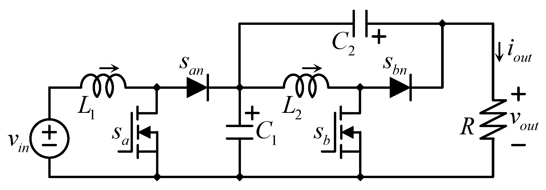
Figure 1 shows the basic configuration of the MSBA converter; it can be extended to more power stages, but this work is focused on the basic one. It is made by
two inductors
L1 and
L2,
two capacitors
C1 and
C2,
two transistors
sa and
sb, and
two diodes
san and
sbn. Considering continuous conduction mode (CCM), a diode closes when its respective transistor opens, and it opens when its respective transistors close, similarly to what happens on the traditional boost converter;
san is the diode of the transistor
sa, and
sbn is the diode of the transistor
sb.
The input voltage is denoted as vin, and the output voltage and current are denoted as vout and iout, respectively. In this article, lower cases represent the large signal of a variable, and upper-case variables represent their DC value or steady state. In other words, the DC components of vin, vout, and iout are Vin, Vout, and Vout, respectively.
2.1. The Duty Cycle
The operation of power converters is manipulated with their transistors’ firing signals, also called switching functions. The MSBA converter has two transistors and two switching functions; it is common to call the switching function the same name as their respective transistors.
If there is a switching signal
sx related to a transistor
sx, the switching functions are a digital function of the time. As other digital functions, it can take only two values (0 or 1), and the operation of the transistor can be described as (1).
The practical implementation of switching functions can be made with digital or analog circuits, in which a certain voltage value is assigned to the digital one value (for example, 5 V), while the digital zero is usually assigned to zero volts.
Then the converters can be driven with the pulse width modulation (PWM) technique, consisting of switching the transistor at constant frequency
FS (hence at a constant switching period)
TS =
1/FS. Let us consider that
sx(0) = 0, and the transition (from 0 to 1) occurs at time
t = dTS (see
Figure 2).
The duty cycle
d is defined as the ratio of the time in which the transistor is closed divided over the total switching period
TS. The duty cycle
d is equivalent to the average value of the switching function, as (2) indicates.
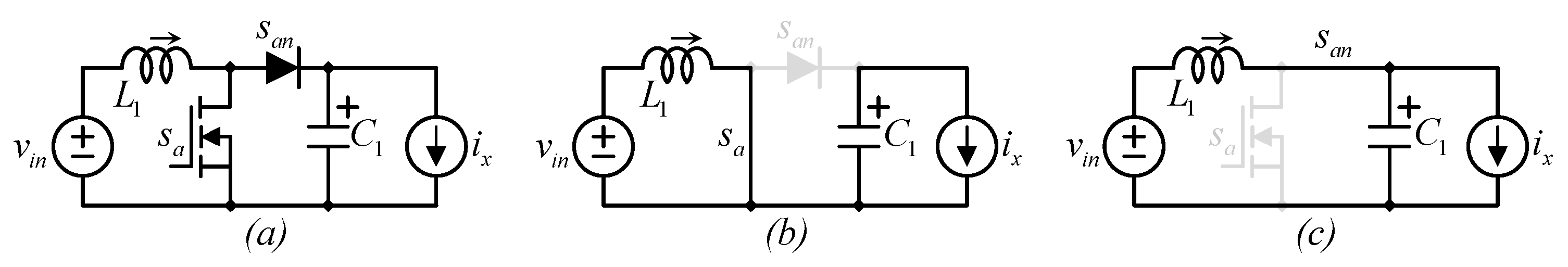
2.2. The First Power Stage
As can be observed from
Figure 1, the MSBA converter in this article can be decomposed into two cascaded power stages (other MSBA converter topologies can contain more than two [
7,
8,
9]). In order to obtain a mathematical model in a relatively simple way, let us analyze the individual power stages, and then we will unify them in the composing converter. The first power stage can be seen as a traditional boost converter. Although their model is well known, it will be explained for understanding the derivation of the model of the second power stage.
Figure 3a shows the traditional boost topology, which is one of the composing power stages of the MSBA converter. The converter has two equivalent circuits in the continuous conduction mode (CCM) [
10].
Figure 3b,c show the equivalent circuits of the boost converter according to the switching state.
Figure 3b shows the equivalent circuit when the transistor (
sa) is closed while the diode (
san) is open.
Figure 3c shows the equivalent circuit when the transistor (
sa) is open while the diode (
san) is closed.
In the first equivalent circuit (see
Figure 3b), the inductor is connected to the input power source, and it is charged while the capacitor is discharged with the current
ix. This can be expressed by (3) and (4).
In the second equivalent circuit (see
Figure 3c), the inductor is connected between the input power source and the capacitor
C1. The capacitor is still being discharged with the current ix, but it also receives the inductor current. This circuit can be expressed by the following equations.
The standard analysis technique for this kind of circuit [
10] consists of averaging (in time) the differential equations by using the definition of the duty cycle as expressed by (7) and (8).
Equations (7) and (8) can be further simplified to (9) and (10).
Equations (9) and (10) are important since the state variables of a converter are current through inductors and voltage across capacitors. The steady state of equilibrium is the operating state reached after the transient. During the transient oscillations can be present on the state variables. The steady state can be defined as the operating condition in which the derivative of state variables is equal to zero [
10]. By invoking the steady state definition in (9) and (10) (in which the derivatives are zero), the equilibrium of the boost converter can be expressed as (11) and (12).
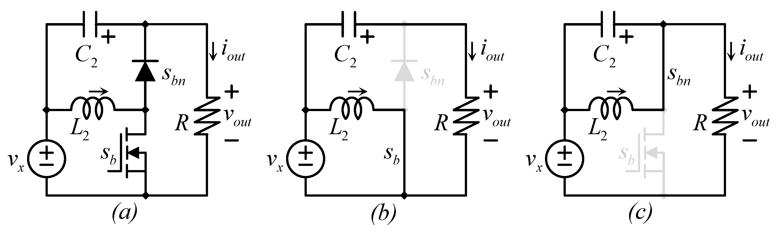
2.3. The Second Power Stage
Let us now analyze the second power stage (see
Figure 4a) with the same procedure. Although the diode is drawn in a vertical position, the circuit in
Figure 4a is basically the second power stage of the MSBA converter. As well as in the previous case, in continuous conduction mode (CCM), the converter in
Figure 4a has two equivalent circuits.
Figure 4b,c show the equivalent circuits of the converter according to the switching state.
Figure 4b shows the equivalent circuit when the transistor (
sb) is closed while the diode (
sbn) is open.
Figure 4c shows the equivalent circuit when the transistor (
sb) is open while the diode (
sbn) is closed.
In the first equivalent circuit (see
Figure 4b), the inductor is connected to the input power source, and it is charged while the capacitor is discharged with the output current (
iout). This can be expressed by (13) and (14).
In the second equivalent circuit (see
Figure 4c), the inductor is connected to the capacitor
C2. The capacitor still is being discharged with the current
ix, but now it also receives the inductor current. This circuit can be expressed by the following equations.
By following the standard averaging technique [
10], the following expressions can be written for the average voltage across the inductor and the average current through the capacitor.
Equations (17) and (18) can be further simplified to (19) and (20) that also consider
vx = vC1.
By using the steady state definition in (19) and (20) (in which the derivatives are zero), the equilibrium of the second power stage can be expressed as (21) and (22).
2.4. The Steady State Full Unified Model
By using (11) and (12), and (21) and (22), a unified steady state model of the converter can be obtained as (23)–(26).
Remind the converters output voltage is equal to
VC1 + VC2 (see
Figure 1), then the output voltage and output current of the converter can be expressed as (27) and (28).
As a last stage in the steady state modeling, the gain
G of the converter, which relates the input voltage to the output voltage (
Vout/Vin), can be expressed as (29).
2.5. Comments about the Model, the PWM, and the Operation of the Converter
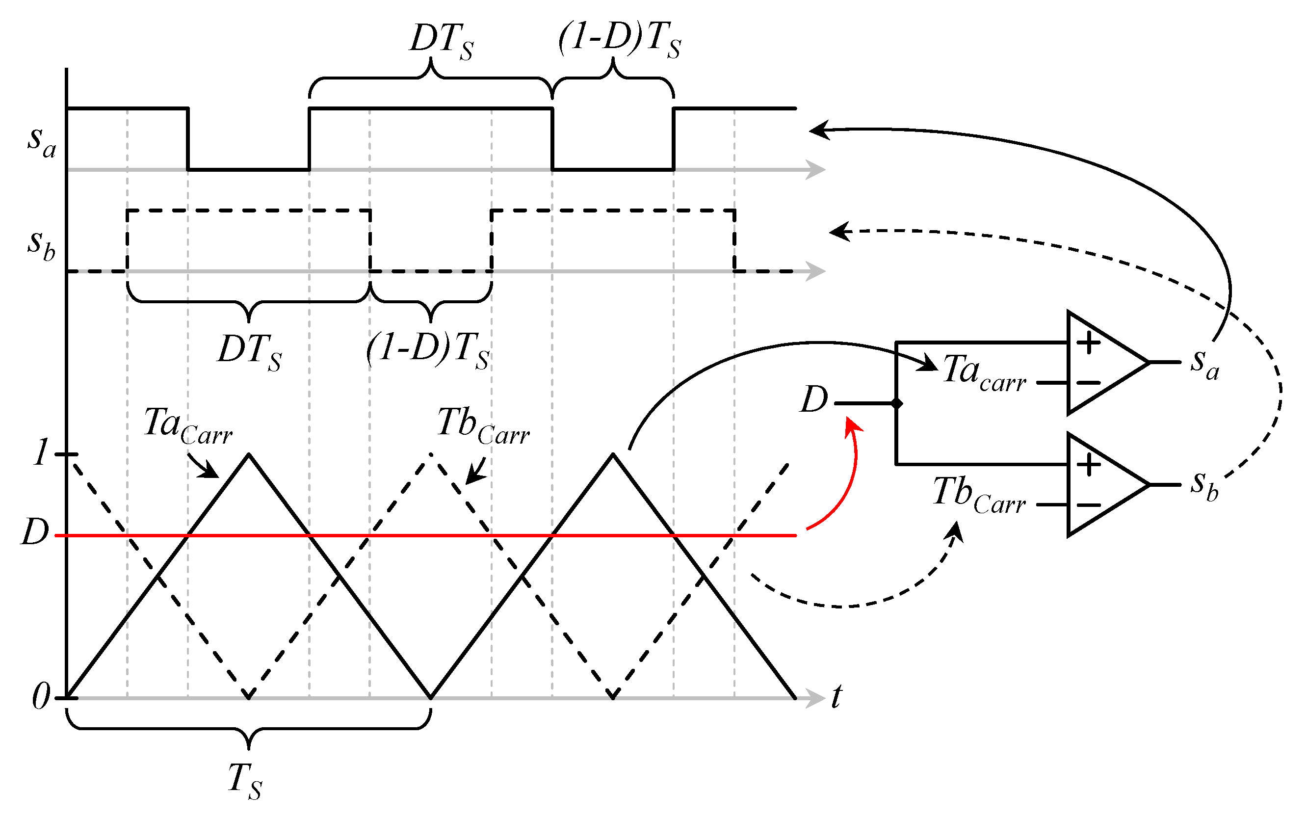
Initial works regarding this converter considered a symmetric operation, meaning both transistors switched with the same gate signal or switching function and open and close simultaneously. It was demonstrated in [
3] that the converters operate better when they have the same duty cycle (in red color) but different switching functions (a phase shift of 180° among them), which is the operation that will be considered in this work. The switching functions of transistors are generated with a type of interleaved pulse width modulation (PWM) scheme.
Figure 5 shows the PWM generator along with important waveforms.
The PWM generator is relatively simple. It consists of two triangle waveform generators and two comparators. The triangle waveforms (Tacarr and Tbcarr) and the duty cycle D (a DC value) are the input signals for comparison. The duty cycle (D) signal is compared to the triangular carriers. The output of comparators is the driving signals. As can be seen, carriers are shifted 180° among them. This phase shift produces the phase shift among the firing signals (sa and sb).
This PWM generator can be implemented with analog circuits, but in modern converters, it is usually produced by a PWM generator made by hardware inside a microcontroller or a digital signal processor (DSP).
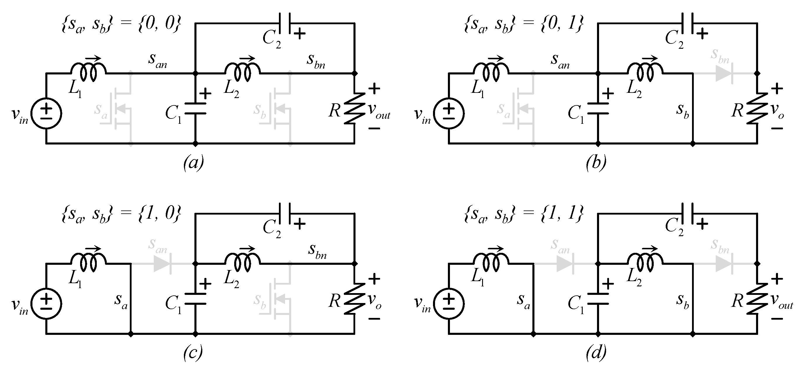
In other words, only one duty cycle is used, but the modulator produces two firing signals. The duty cycle is the same for both transistors, which means they are closed at the same average time but have different switching functions. Each switching function is a digital signal that indicates if its respective transistor is open or closed. Then, in the operation, there are four possible combinations of switching functions; those combinations are
{sa, sb} = {0, 0}, {0, 1}, {1, 0}, or
{1, 1}.
Figure 6 shows the equivalent circuits of each switching state.
As explained in [
3], the number of equivalent circuits is four, but the number of circuits that appear during the operation may be two (when
D = 0.5) or three (when
D ≠ 0.5). The duty cycle
D is adjusted by the voltage regulator in case there is a change in the input voltage or the load.
Regardless of the number of switching states, or equivalent circuits, the voltage of each inductor depends only on the position of their respective transistor (sa to L1 and sb to L2). During a switching period, any transistor stays closed for a period of DTS and stays open for a period of (1-D)TS. Then, the average voltage in inductors, which are the base for some of the state equations of the converter, can still be expressed as (9) and (19).
2.6. The Output Voltage Ripple
The optimization explored in this article is closely related to the output voltage ripple of the converter. This is a measure of the power quality delivered by the converter. It is well known that it can be improved with larger capacitance in capacitors since this increases the stored energy. However, the article’s purpose is to minimize the output voltage ripple for a certain amount of stored energy (the increase of the stored energy can be combined with the optimization to improve further).
The output voltage ripple effect is explained in detail in [
3]. It is important to mention that the maximum ripple can be generated in two different equivalent circuits, actually depicted in
Figure 6b,c (
{sa, sb} = {0, 1} or
{sa, sb} = {1, 0}); since the circuit has two rising output voltage states, the output voltage ripple of those equivalent circuits is expressed in (30) and (31).
The optimization objective must be to minimize the larger value among (30) and (31). The differential evolution algorithm performs minimizations of (30) and (31), which is described in
Section 3.
3. The Optimization Algorithm
The proposed strategy aims to optimize the capacitance values of two capacitors, C1 and C2, for the MSBA converter in order to reduce the output voltage ripple of this converter. Therefore, an optimization algorithm can be implemented to reduce these capacitance values.
Although there is a large number of optimization algorithms ranging from classic algorithms (such as the firefly algorithm (FA) [
11], the particle swarm optimization algorithm (PSO) [
12], the artificial bee colony (ABC) [
13], and others), and even more recent ones (such as the arithmetic optimization algorithm (AOA) [
14], the red fox optimization (RFO) [
15], and the aquila optimizer (AO) [
16], to mention a few), we propose the use of the classic differential evolution (DE) algorithm [
17].
The DE method has been chosen because it is one of the most significant and popular optimization algorithms, due to its easy implementation and high performance in finding optimal solutions even in constrained optimization problems [
18], such as the one proposed in this work.
The DE algorithm is a popular and extensively used method for solving complex optimization problems. It has attractive characteristics such as low complexity and high performance, making it a classic and broadly used application in different fields. Some applications of the DE include image processing, electronics engineering, operation research, manufacturing design, mechanical engineering, and power engineering, to mention a few [
18]. The DE algorithm preserves its distinction in the metaheuristic community even though there are other classic metaheuristic algorithms or other sophisticated evolutionary methods recently proposed in the literature. Its popularity is primarily because of its low computational cost, easy implementation, and efficiency, even in high-dimensional and constrained optimization problems [
19]. Therefore, the DE algorithm is used in the optimization process of the presented work.
Therefore, the DE algorithm is chosen to find the optimal values of the capacitors, and it is briefly introduced in this section.
3.1. The Differential Evolution Algorithm
The DE algorithm is considered an evolutionary method that uses particles as potential solutions to search for a fitness function’s minimum or maximum value that represents the optimization problem. The first step of the DE method is to initialize the particles within a limited search space as follows:
Here, every particle i is represented as and generated randomly between the lower and upper bounds. The optimization problem defines these limits. After initialization, the main operators of the DE are executed in an iterative process. These operators are mutation, crossover, and selection.
3.1.1. Mutation
The mutation operation is used to generate mutant vectors based on the existent candidate solutions. The mutant vectors are created under the combination of three particles randomly selected from the population. This combination creates vectors that have the shared information of the three particles. The main goal of the mutation operation is to exchange feature information to generate better candidate solutions during the crossover process. The definition of the mutation operator is as follows:
where
is the mutant vector while
,
, and
are the particles randomly selected from the population. In addition,
b is the differential weight that ranges from
0 to
2 and controls the magnitude of the difference between
, and
.
3.1.2. Crossover
The crossover operation is applied to generate new possible solutions based on the selection of some of the features from the mutant vectors and some from the actual particles. This operation ensures there exists diversity among the population. The crossover involves selecting one feature from the mutant vector according to a certain crossover probability
Cprob or one feature from the current particle if this probability is not reached. This way, a new candidate solution is built by selecting features from the mutant vector or the current particle, depending on this stochastic process. The crossover operation is defined as follows:
where
denotes the feature
j of the new possible solution, and its value is selected between the values of features
and
from the mutant vector
and the actual solution
, respectively. The selection is performed by evaluating if a random value is equal to or lower than the crossover probability
Cprob. The function of the crossover probability is to regulate the contribution of the mutant vector in the creation of the possible solution that may be selected to be part of the new generation.
3.1.3. Selection
The selection operator eliminates the worst candidate solutions and keeps the best to create a new population that evolves in every generation. The selection is based on the fitness values of the solution created in the crossover process and the current solution. The particle that has the best fitness value will remain in the population for the next generation, while the other is eliminated. The selection operation is described as follows.
where
denotes the new and the best candidate solution that will be part of the next generation
k + 1. The current solution is
, while the solution created in the crossover process is
and the fitness values of this solution are
and
, respectively.
4. Design Example and Optimization
To introduce the optimization process, a design example will be discussed. The design considers an MSBA converter in which inductors are
L1 = 100 µH and
L2 = 100 µH; the switching frequency is selected as
FS = 50 kHz. Let us consider that the input of the MSBA converter ranges from 20 V to 25 V, and the converter must provide a regulated voltage of 200 V. The current changes linearly; when the source voltage is 20 V, the source current is 10 A, and when the source voltage is 25 V, the source current is 2 A. Those values are not unusual; they are similar to the application in which the converter is fed by a fuel cell (FC), and the converter feeds a grid-tie inverter. Parameters are not obtained from a particular FC, but several commercial FC can be referred to; for example, see FCS-C200 from [
20].
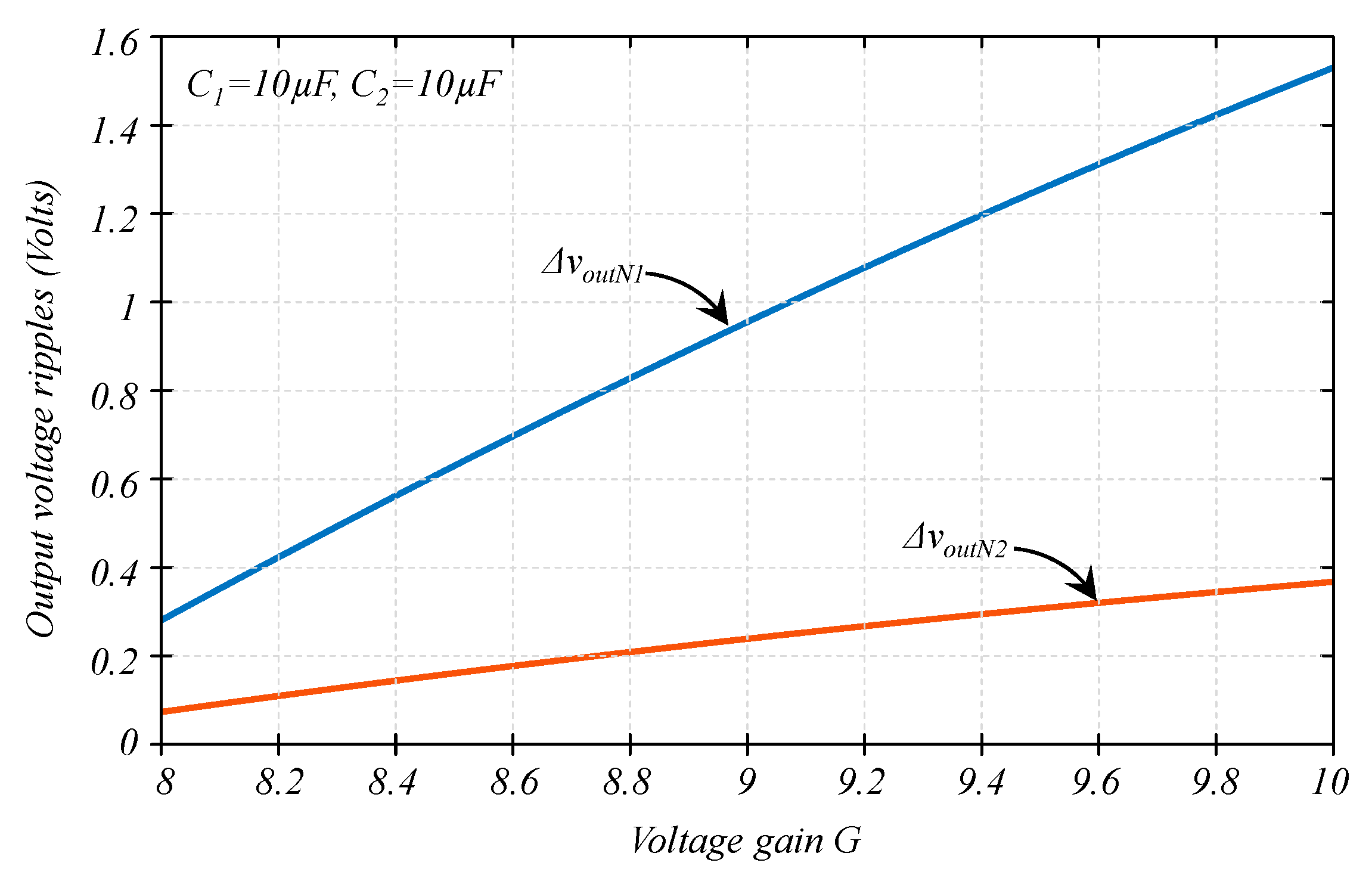
Let us consider a design
Option A, in which capacitors are equal to
C1 = 10 µF and
C2 = 10 µF, considering equal capacitors may be a very common starting point, as introduced in [
3]. The evaluation of the equation of the output voltage ripple (Equations (30) and (31)) along the gain-range operation would result in
Figure 7.
From
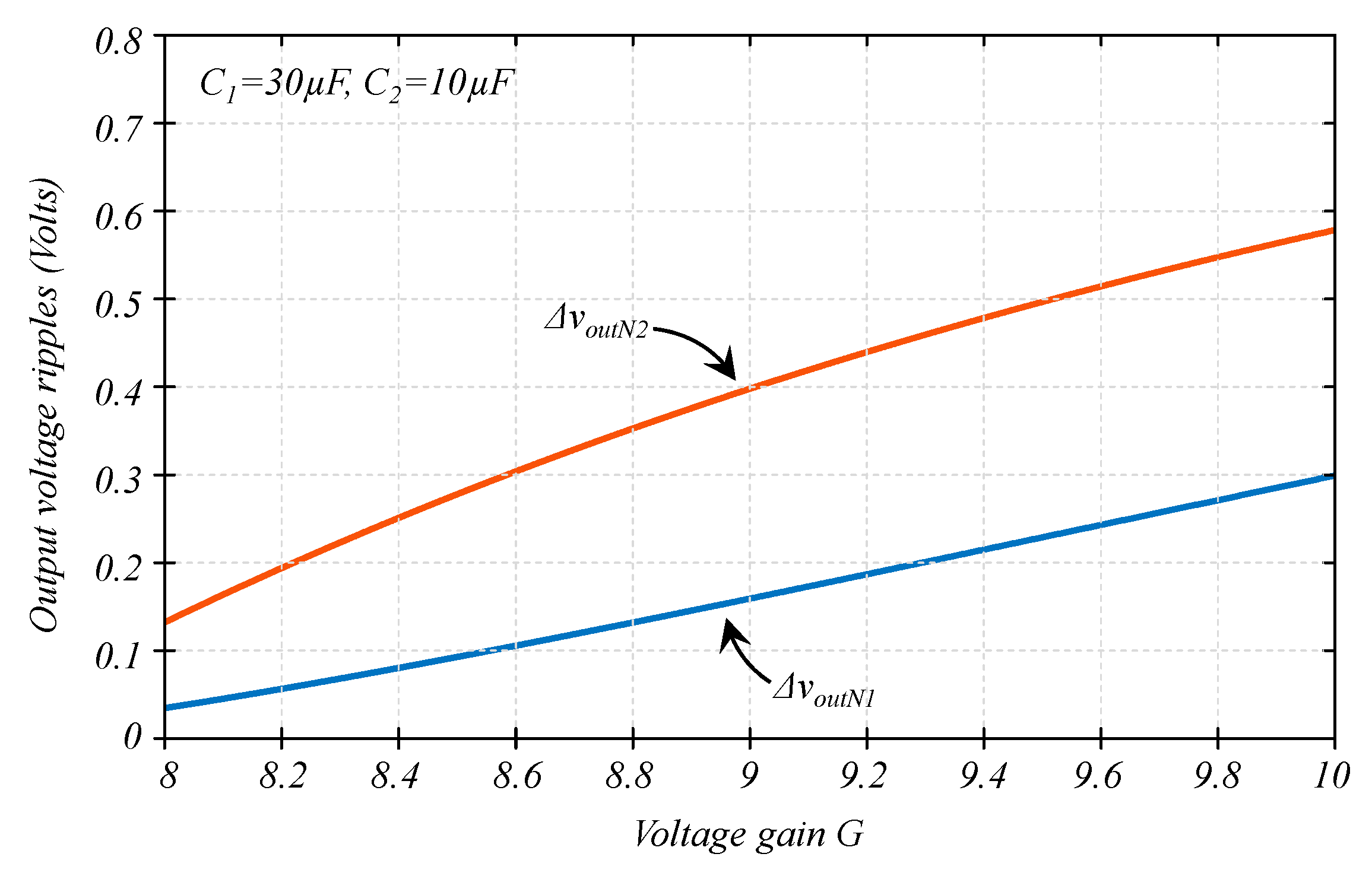
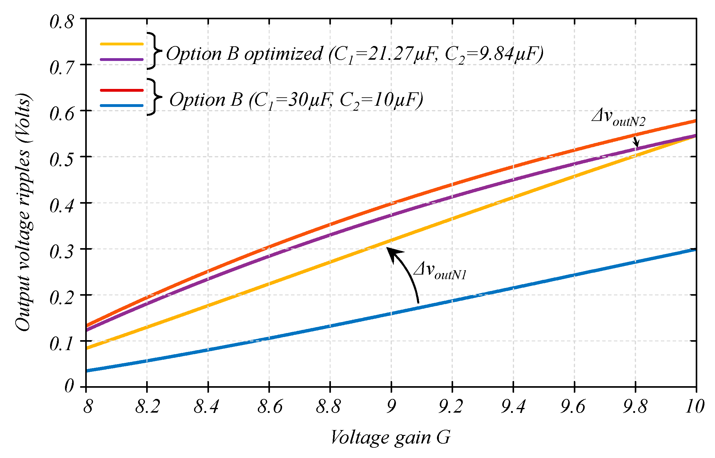
Figure 7, we can observe that the output voltage ripple is fully determined by (30) since (31) provides a smaller value for the full operation range; on the other hand, this does not mean we can ignore (31), because another combination of capacitors may provide a totally different result. For example, let us consider an Option B in with
C1 = 30 µF and
C2 = 10 µF. It was previously shown in [
3], that a selection on different capacitors may change the relation among Δ
voN1 and Δ
voN2, but [
3] used a different relationship. The evaluation of the output voltage ripple (Equations (30) and (31)) would result in
Figure 8.
It is evident from
Figure 8 that in some cases, (31) may provide a larger value than (20), and then it cannot be ignored.
We can observe that the output voltage ripple in
Option B is much smaller than in
Option A.
Figure 7 shows a maximum of around 1.5 V against
Figure 8, which shows a maximum of less than 0.6 V. However, on the other hand, the capacitance cannot be arbitrarily increased since the capacitance is proportional to the stored energy in capacitors, which is also proportional to the size (volume) of capacitors [
4,
21,
22,
23,
24], if the capacitance is too large, the converter may be undesirably large.
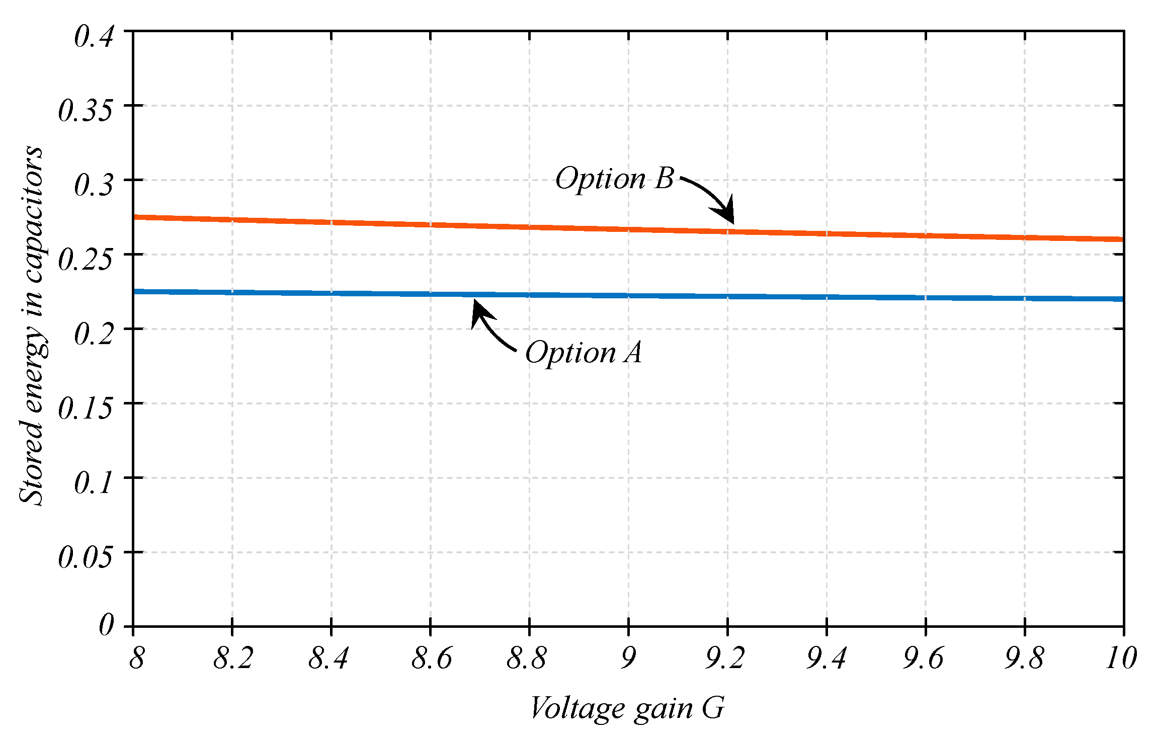
The energy stored in capacitors can be expressed as (36).
The voltage across capacitors changes depending on the operating condition.
Figure 9 shows the evaluation of (26) for both
Options A and
B of the discussed problem.
As expected, Option B, in which the capacitance of C1 is twice that of Option A (all other components are equal), results in larger stored energy, but the increase of the stored energy is not substantial. The stored energy increased by 22%, but the output voltage ripple is reduced by more than 60%.
4.1. The Optimization Problem
The problem consists of choosing values for the capacitance of
C1 and
C2 that minimizes the maximum value given by (30) or (31), repeated here as (37) and (38) (the larger of them), but not overpassing a maximum of stored energy (36), repeated here as (39).
Currents
IL1,
IL2, and
Iout are defined in (25) and (26),
VC1 and
VC2 are defined in (23) and (24), and the duty cycle
D can be obtained from the gain range, for example, in this case, the output voltage is regulated to µ0V, while the input voltage ranges from 20 to 25 V, this produces the voltage gain
G to range from 8 to 10. The duty cycle for a particular operation point can be derived from (29) and calculated from (40).
The result will be provided in the exact value (with decimals); although the exact solution is not commercial, it can give a good approximation to the commercial value.
The maximum stored energy in capacitors coincides with the minimum voltage gain (see
Figure 9). It is 225 mJ for
Option A and 275 mJ for
Option B.
Let us consider two cases, the first one in which the maximum stored energy of 225 mJ and the second one in which the maximum stored energy is 275 mJ.
According to the optimization problem formulated above, the fitness function
f is defined as the minimization of the maximum value between Equations (37) and (38) as follows:
The fitness function includes one constraint that ensures the maximum stored energy Jcaps is accomplished. This value changes depending on what option (A or B) is being simulated. Furthermore, the values of the two capacitors (C1 and C2) are restricted with a minimum and maximum possible value. These values range from 0 to a maximum capacitance in which a single capacitor stores the allowed stored energy (leaving no stored energy capacity available for the second capacitor) since higher values will overpass the maximum stored energy constraint.
4.2. The Simulation
The DE algorithm is used in the simulation to find the optimum values of capacitors
C1 and
C2. The optimization process involves particles with two features, each corresponding to possible capacitance values for the capacitors. Thus, every particle from the population is defined as:
In the initialization step, a population of 50 particles is created within the interval of [0, 30 × 10−6]. Later, the mutation and the crossover operation are carried out. Then, the selection process is made. Every particle is evaluated in the objective function to compare the quality of the current particles and the new ones generated in the crossover operation. The particles with the best fitness value will be selected. The chosen particles represent solutions (pairs of capacitance values) that generate lower output voltage ripples.
A penalty function is included in the objective function to ensure that the constraint is accomplished for every candidate solution. The penalty function increases the fitness value of every particle that exceeds the maximum stored energy. Thus, the fitness function can be redefined as follows:
where
p is the penalization added to the fitness function to increase this value if the particle is unfeasible. The penalty function is expressed as:
where
φ is the activation function that allows the penalization when the constraint is violated. On the other hand, when the stored energy requirements are reached, the activation function disables the penalty, so the particle’s fitness is not increased. The activation function is expressed as follows:
With this mechanism, unfeasible solutions are discarded, so the optimization process is conducted toward feasible solutions in an iterative process. Thus, the mutation, crossover, and selection operators are applied to every particle until a maximum number of generations is reached. In the simulations, we use a maximum of
500 generations. The parameter values used in the simulations for options A and B are summarized in
Table 1:
Finally, when the optimization process finishes, every option (A and B) is expected to have the optimum pair of capacitance values for C1 and C2 in the best-found solution so far.
4.3. The Solution
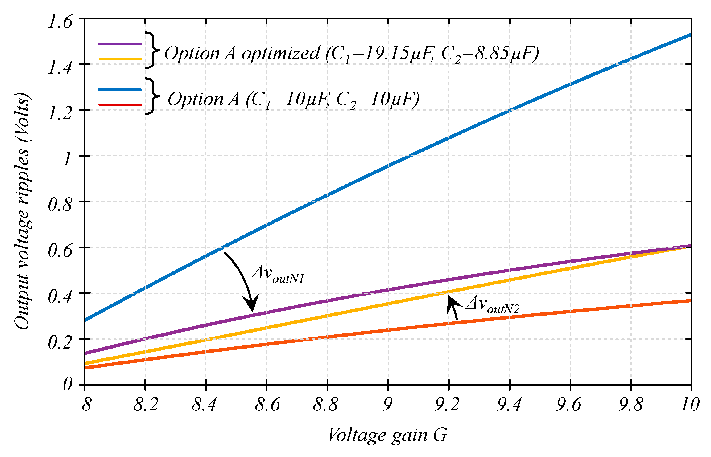
For the case in which the maximum stored energy is
225 mJ, the optimized solution is
C1 =
19.15 µF and
C2 =
8.8563 µF. Similarly to
Figure 7,
Figure 10 shows the output voltage ripple (from both Equations (20) and (21), but in this case, it includes the optimized solution. It seems the graphics of the voltage ripple tends to approach each other. The maximum output voltage ripple turns out to be
0.6069 V. A reduction of 60% against
Option A, in which the maximum output voltage ripple was
1.5298 V.
For the case in which the maximum stored energy is
250 mJ, the optimized solution is
C1 = 21.27 µF and
C2 = 9.84 µF. Similar to
Figure 8,
Figure 11 shows the output voltage ripple from both Equations (20) and (21), but in this case, it includes the optimized solution. Similar to
Figure 10, graphics of the voltage ripple tends to approach each other. The maximum output voltage ripple turns out to be
0.5462 V, a reduction of
5.5% against
Option B, in which the maximum output voltage ripple was
0.5784 V.
In this second case, the reduction is not as substantial as in the first case, but it shows how the optimization process can help ensure the design is well done.
4.4. The Computational Time
The experiments were implemented using MATLAB
® R2022a in a computer with an Intel
® Core™ i7-8550U CPU @ 1.80 GHz 1.99 GHz. The experimental simulation considers 30 independent executions where the elapsed time in seconds has been recorded in every execution. The mean elapsed time considering the 30 executions and the best and worst elapsed time among the 30 executions are reported in
Table 2. From these results, it is evident that the elapsed time is small enough to be depreciated. Thus, optimized options A and B are suitable for computational time consumption.


