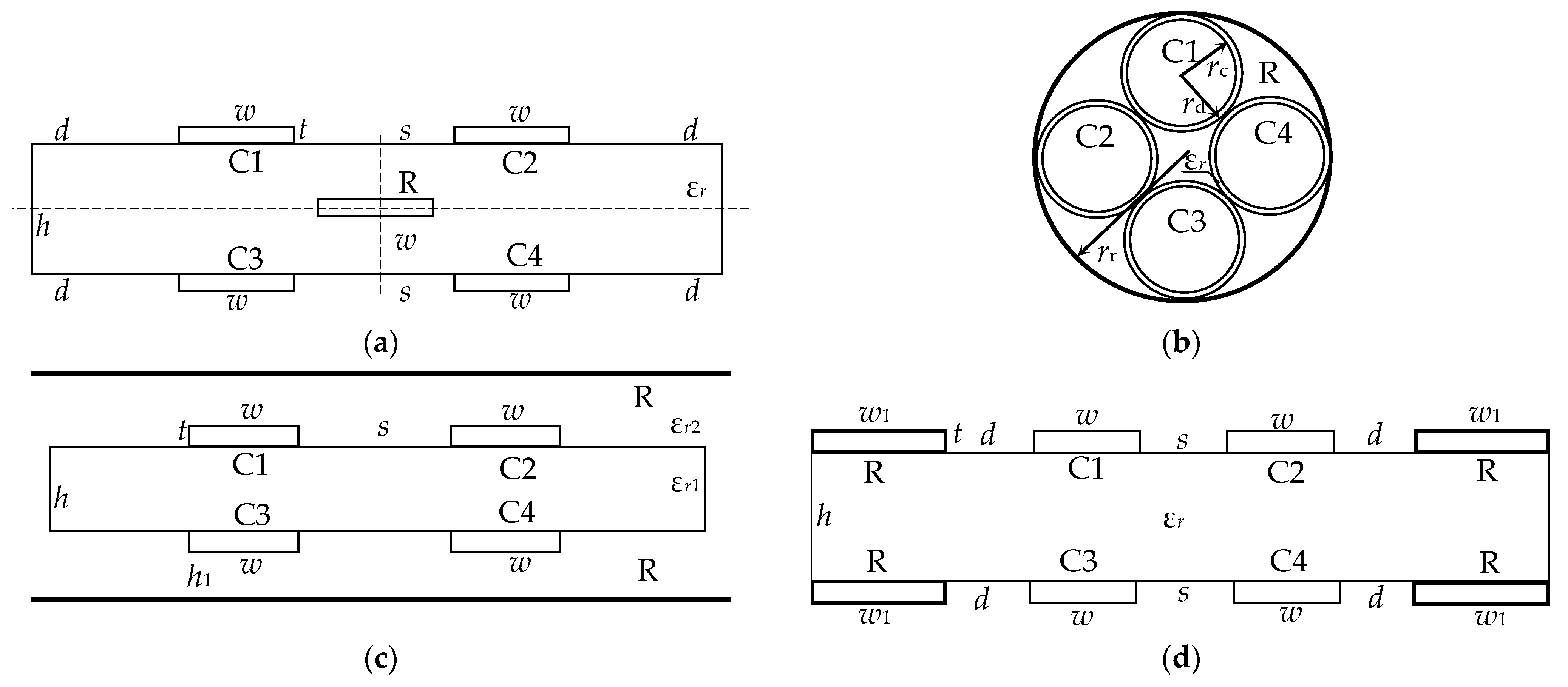
Figure 1.
Cross-sections of structures with the reference conductor (a) in the center, (b) around, (c) above and below, and (d) in the form of side polygons, where conductor C1—active; C2, C3, C4—passive; and R—reference.
Figure 1.
Cross-sections of structures with the reference conductor (a) in the center, (b) around, (c) above and below, and (d) in the form of side polygons, where conductor C1—active; C2, C3, C4—passive; and R—reference.
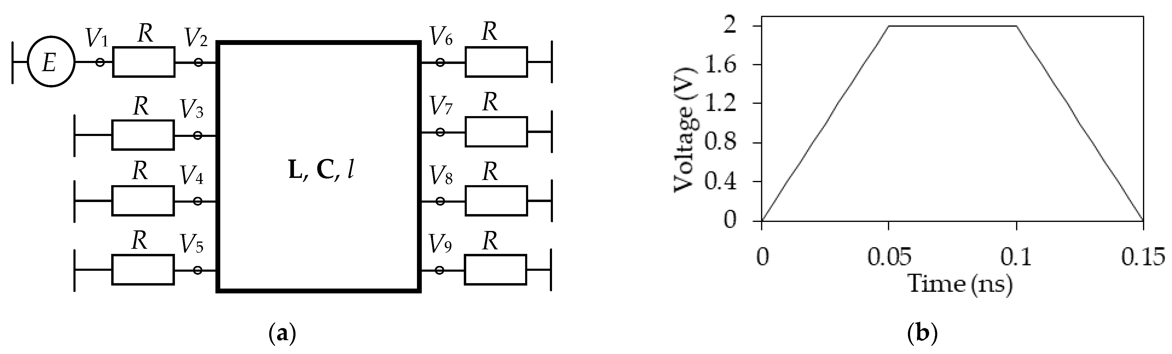
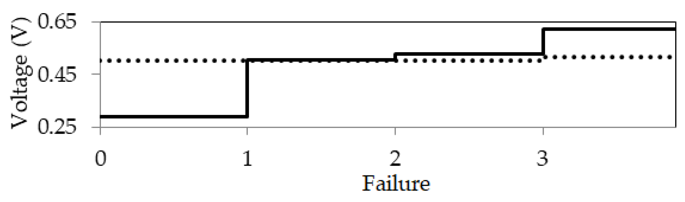
Figure 2.
(a) Equivalent circuit of the structures under consideration and (b) EMF waveform.
Figure 2.
(a) Equivalent circuit of the structures under consideration and (b) EMF waveform.
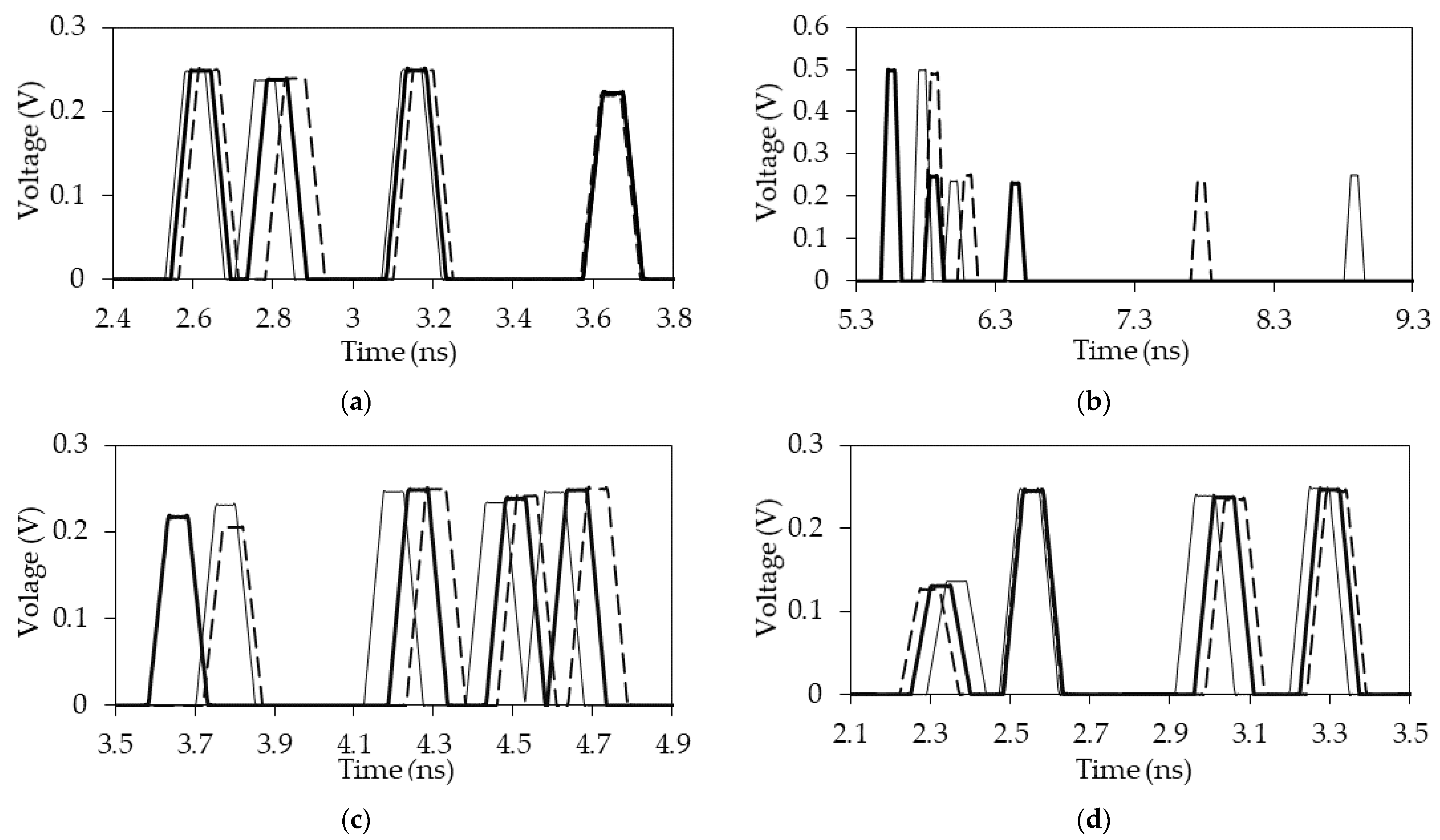
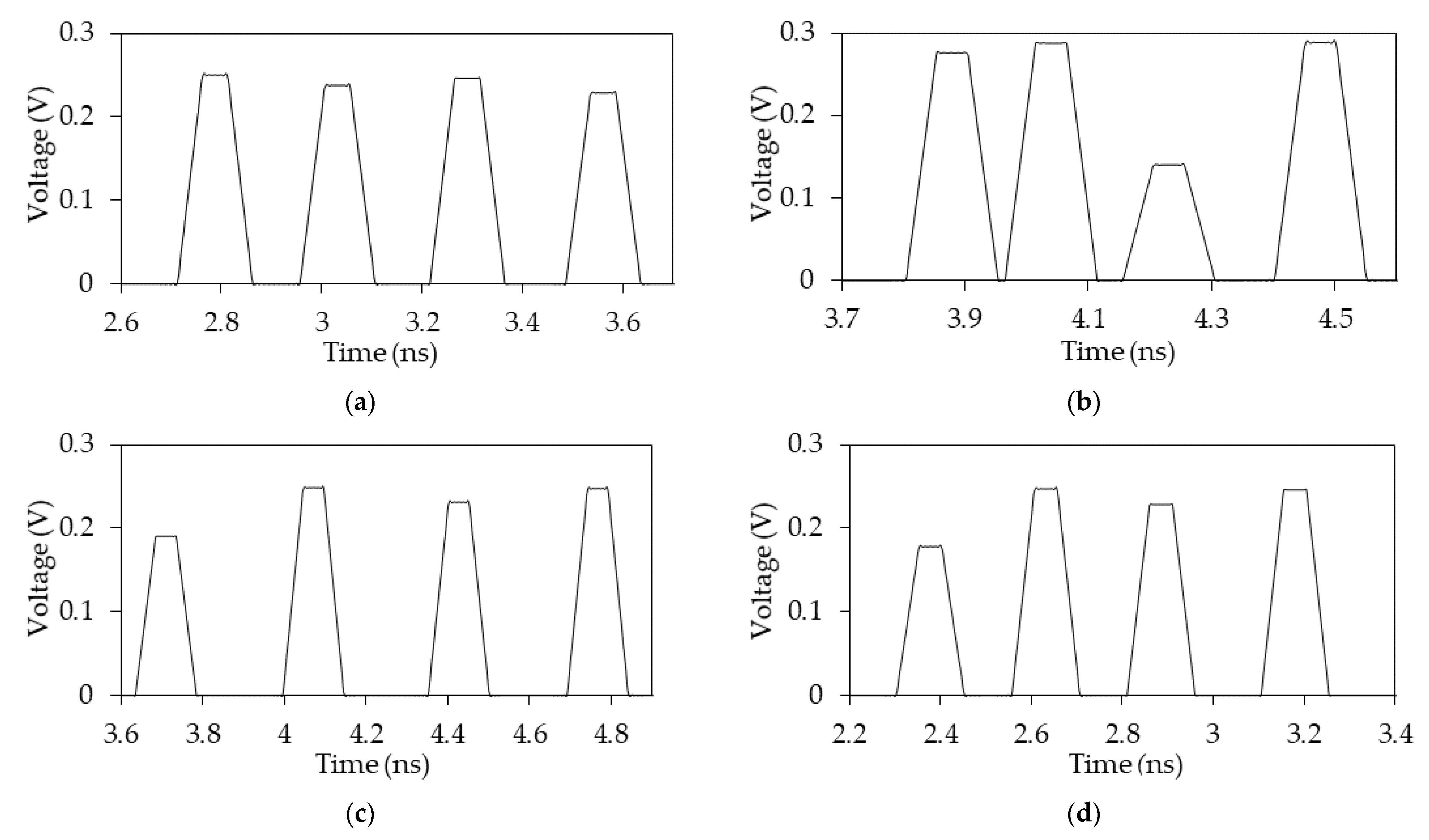
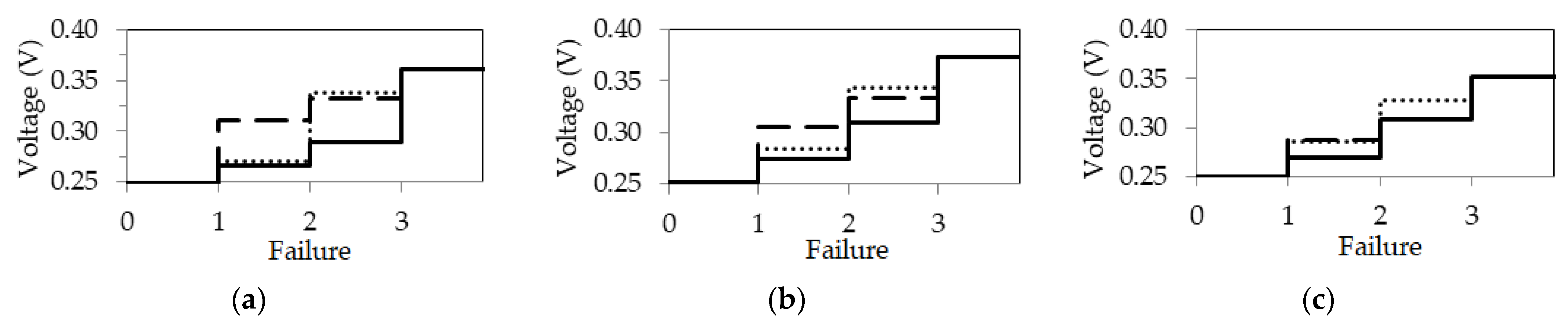
Figure 3.
Output voltage waveforms for the structures with the reference conductor (a) in the center, (b) around, (c) above and below, and (d) in the form of side polygons with parameter sets 1 (––), 2 (––), and 3 (– –).
Figure 3.
Output voltage waveforms for the structures with the reference conductor (a) in the center, (b) around, (c) above and below, and (d) in the form of side polygons with parameter sets 1 (––), 2 (––), and 3 (– –).
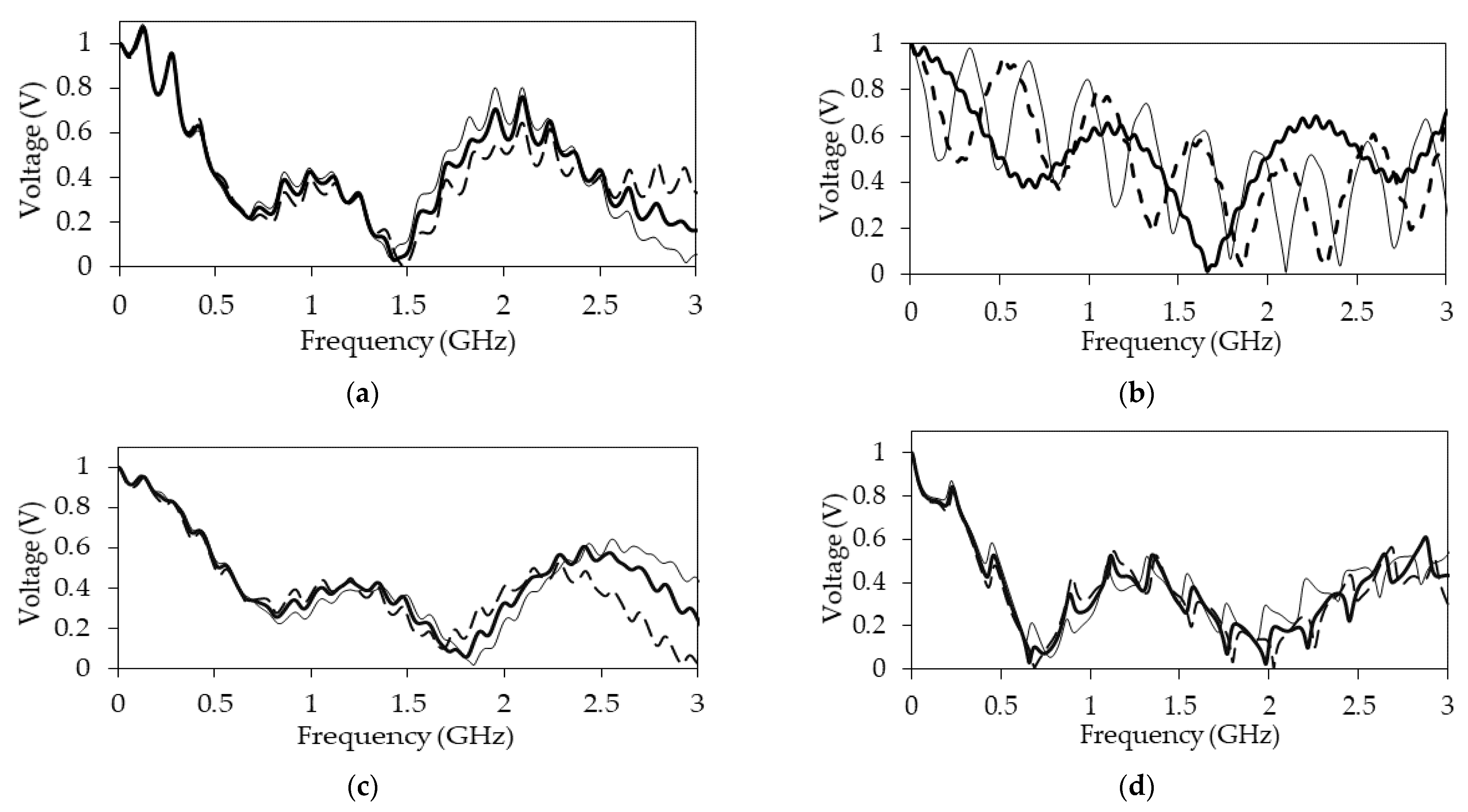
Figure 4.
Frequency responses of structures with the reference conductor (a) in the center, (b) around, (c) above and below, and (d) in the form of side polygons with parameter sets 1 (––), 2 (––), and 3 (– –).
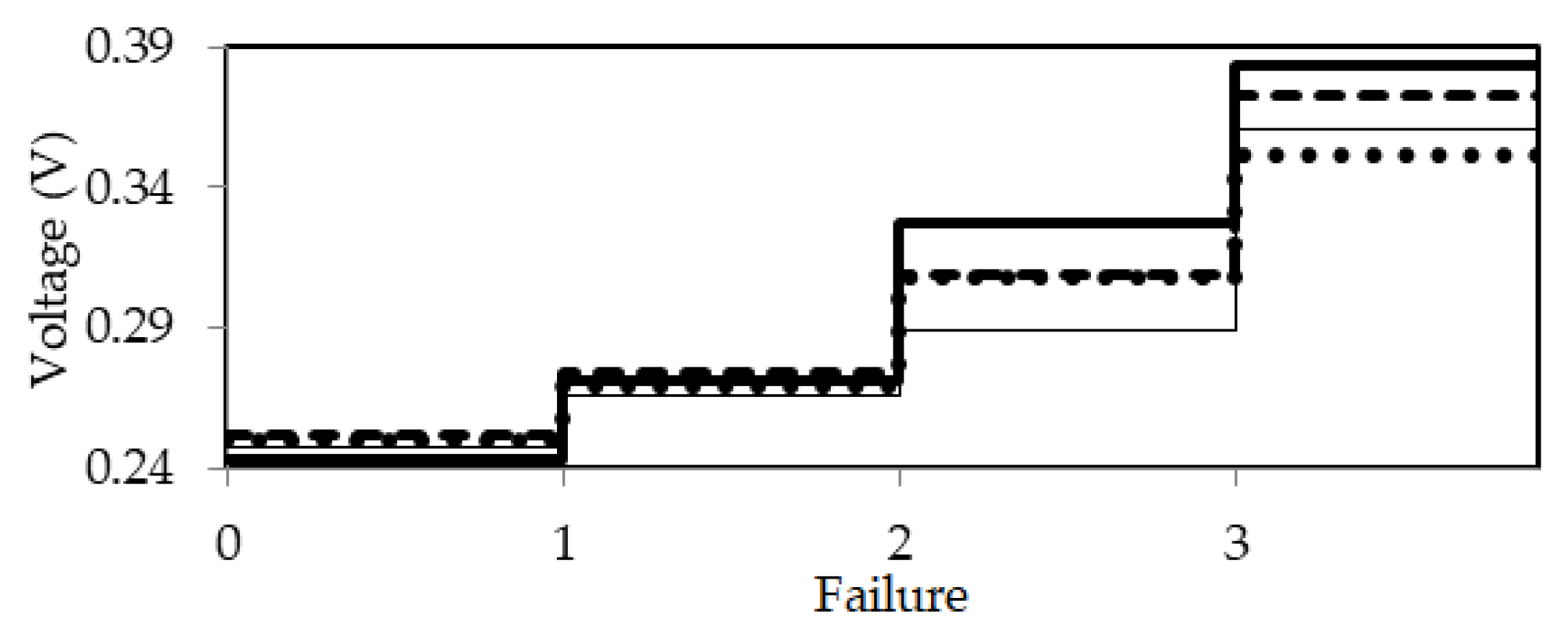
Figure 4.
Frequency responses of structures with the reference conductor (a) in the center, (b) around, (c) above and below, and (d) in the form of side polygons with parameter sets 1 (––), 2 (––), and 3 (– –).
Figure 5.
Voltage waveforms at the output of the structures with a reference conductor (a) in the center, (b) around, (c) above and below, and (d) in the form of side polygons after optimization.
Figure 5.
Voltage waveforms at the output of the structures with a reference conductor (a) in the center, (b) around, (c) above and below, and (d) in the form of side polygons after optimization.
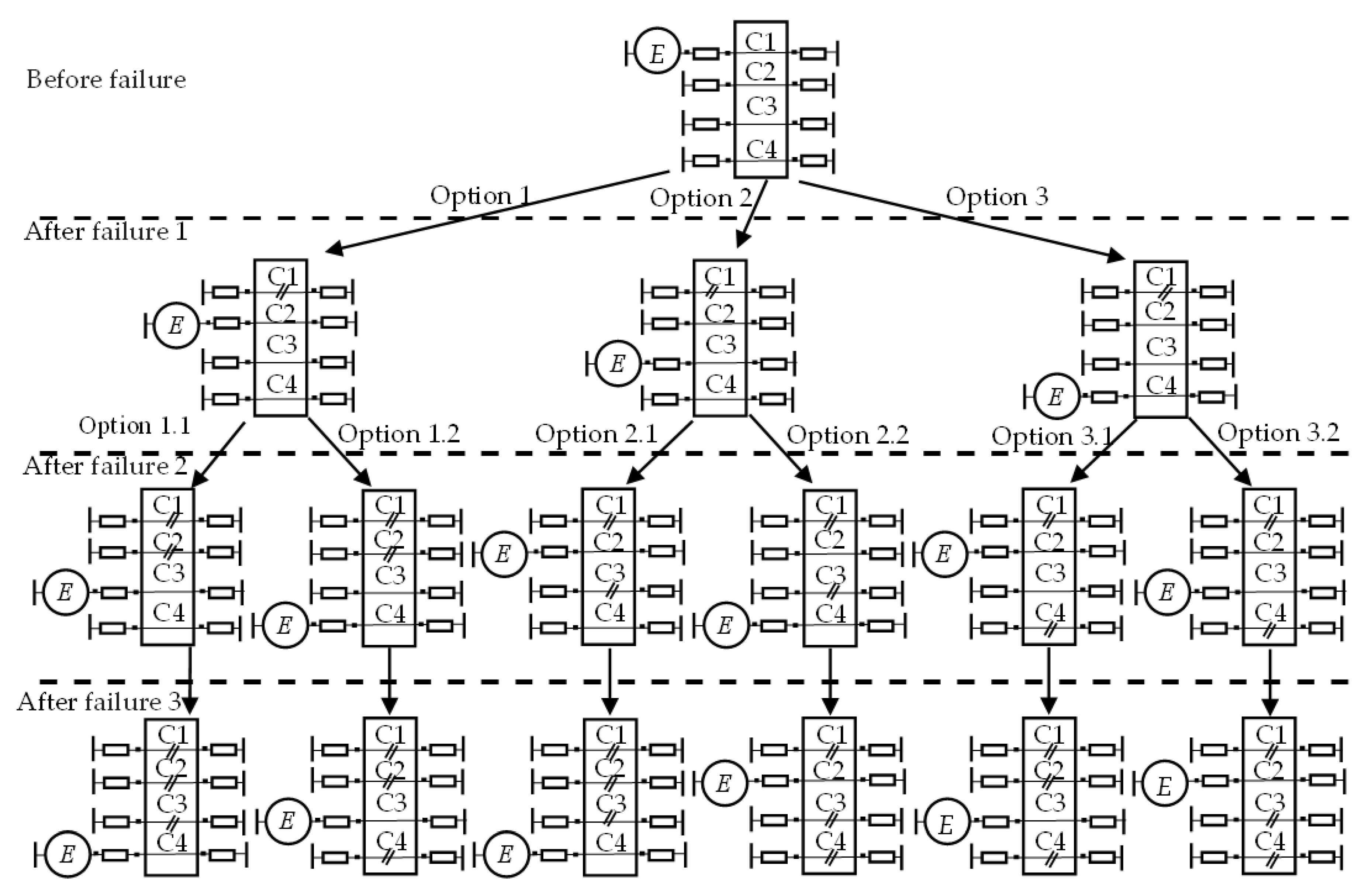
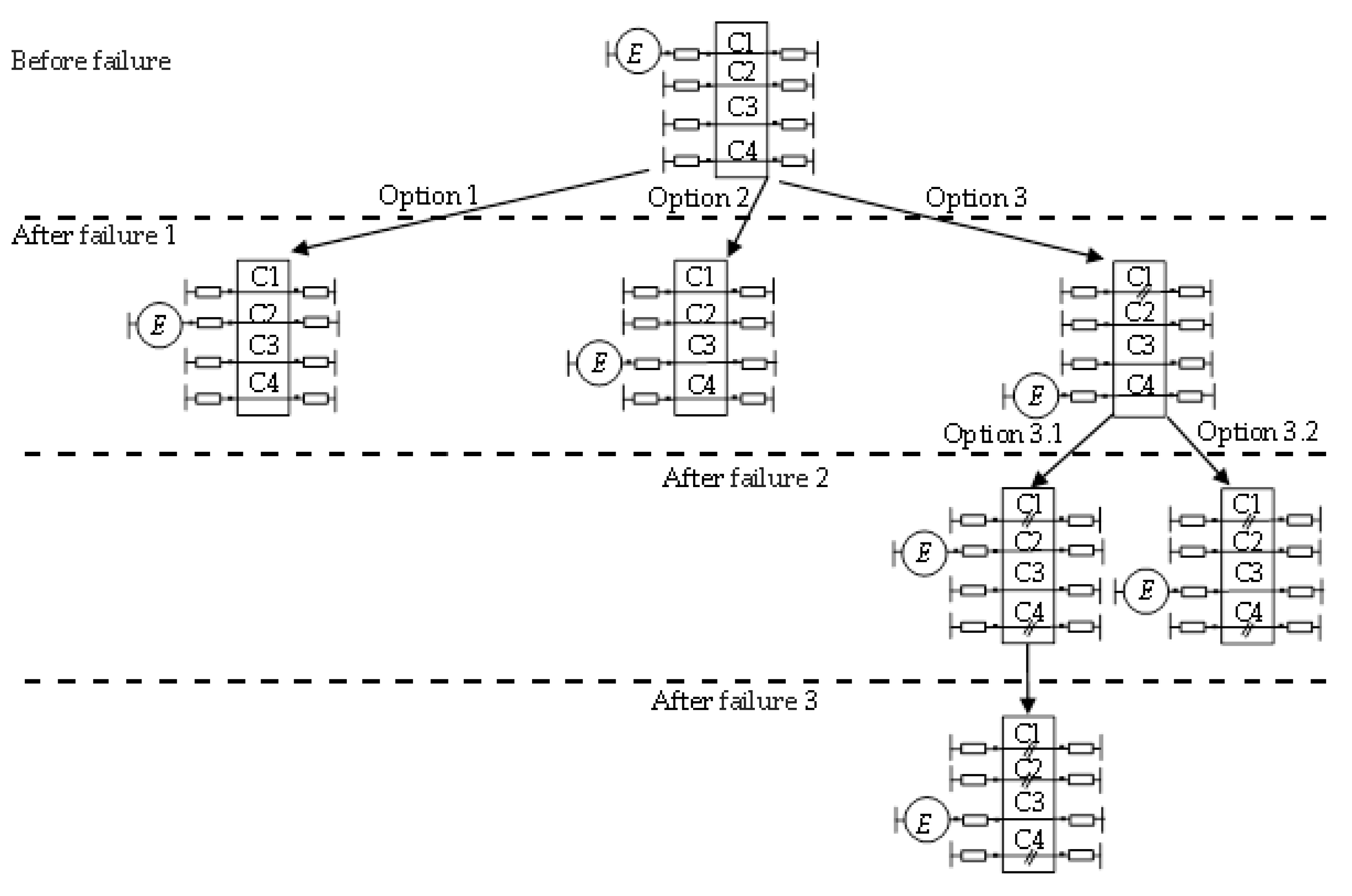
Figure 6.
Options for selecting another active conductor after sequential failures at one end of the active conductor for a structure with triple MR.
Figure 6.
Options for selecting another active conductor after sequential failures at one end of the active conductor for a structure with triple MR.
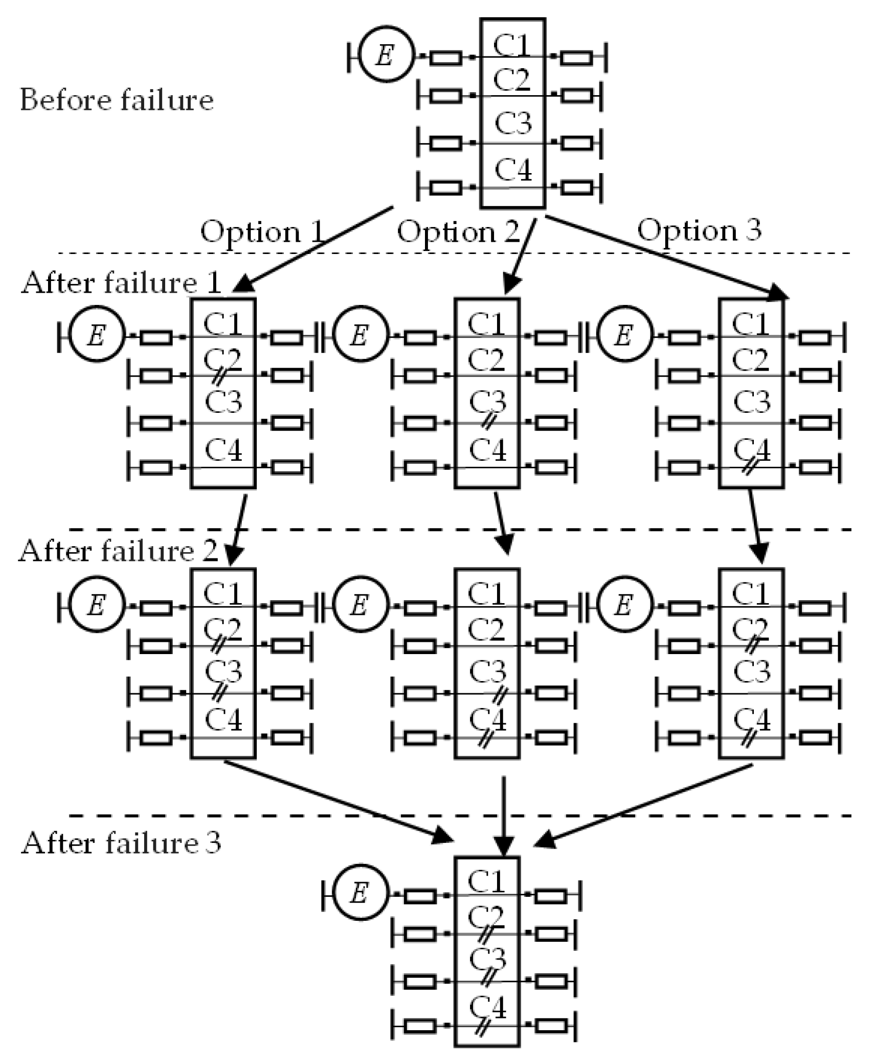
Figure 7.
Equivalent circuit that simulates sequential failures at one end of the active conductor for symmetric structures with triple MR (each failed conductor is an active conductor before a failure).
Figure 7.
Equivalent circuit that simulates sequential failures at one end of the active conductor for symmetric structures with triple MR (each failed conductor is an active conductor before a failure).
Figure 8.
Voltage waveforms at the far end of C1 under different boundary conditions at the ends of (a) C2, (b) C3, and (c) C4 (after failure 1).
Figure 8.
Voltage waveforms at the far end of C1 under different boundary conditions at the ends of (a) C2, (b) C3, and (c) C4 (after failure 1).
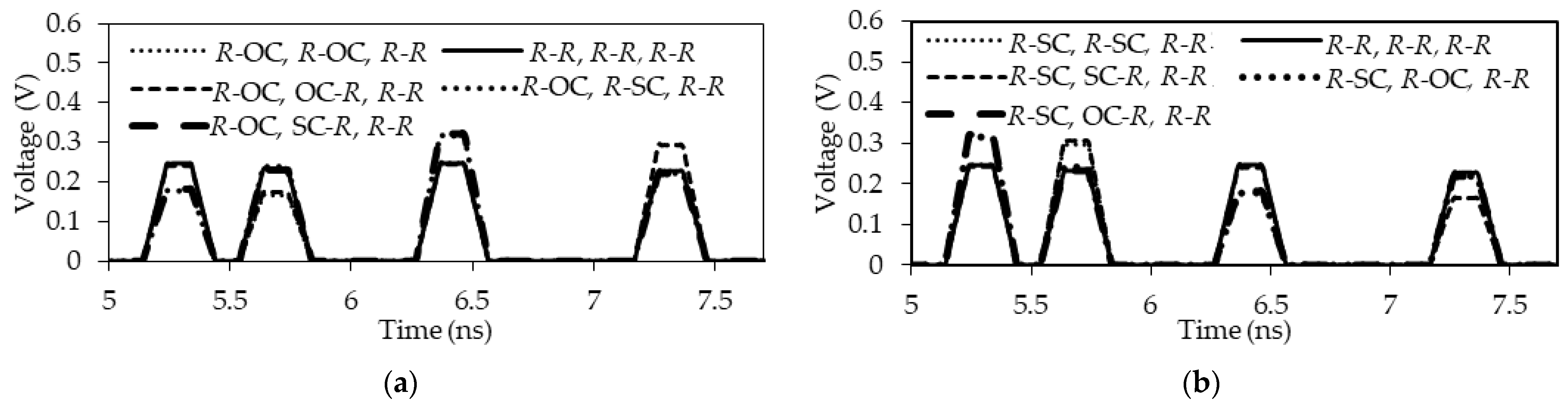
Figure 9.
Voltage waveforms at the far end of C1 with (a) OC and (b) SC at the far ends of C2 and different boundary conditions at the end of C3 with option 1 (after failure 2).
Figure 9.
Voltage waveforms at the far end of C1 with (a) OC and (b) SC at the far ends of C2 and different boundary conditions at the end of C3 with option 1 (after failure 2).
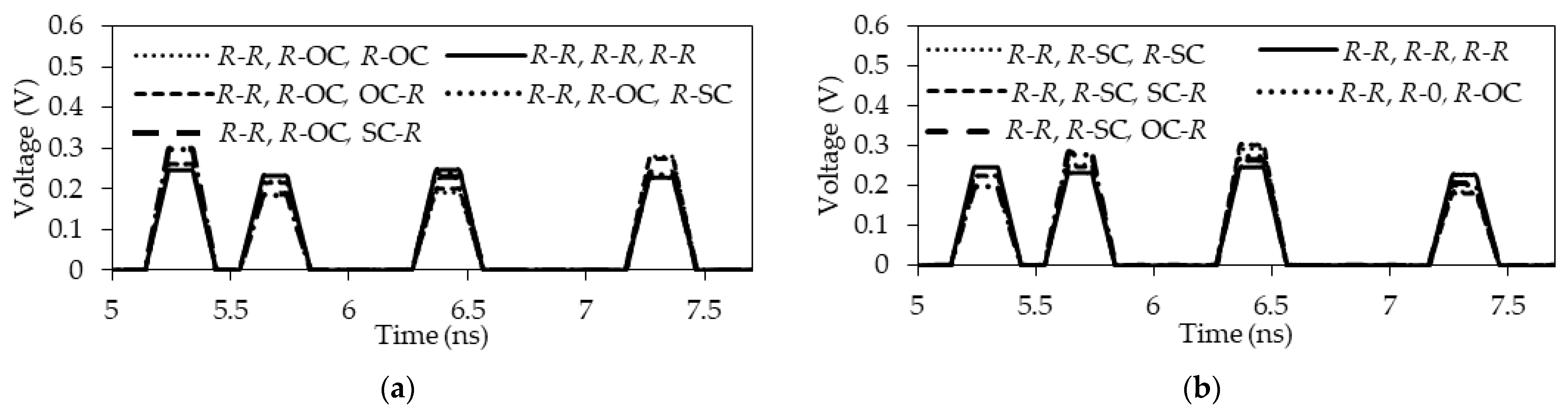
Figure 10.
Voltage waveforms at the far end of С1 with (a) OC and (b) SC at the far end of С3 and different boundary conditions at the ends of С4, with option 2 (after failure 2).
Figure 10.
Voltage waveforms at the far end of С1 with (a) OC and (b) SC at the far end of С3 and different boundary conditions at the ends of С4, with option 2 (after failure 2).
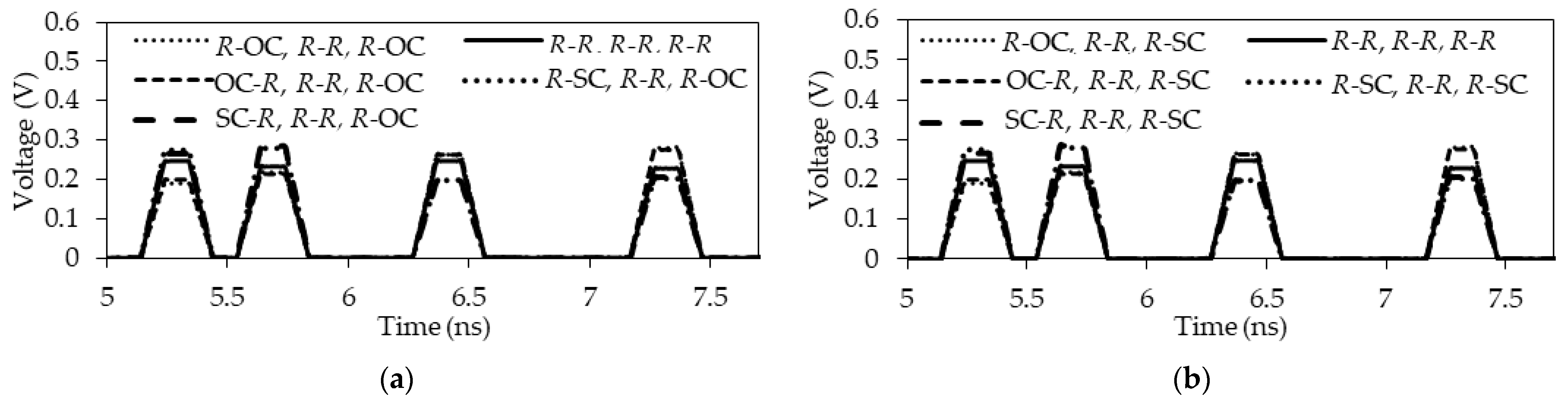
Figure 11.
Voltage waveforms at the far end of C1 with (a) OC and (b) SC at the far end of C4 and different boundary conditions at the ends of C2, with option 2 (after failure 2).
Figure 11.
Voltage waveforms at the far end of C1 with (a) OC and (b) SC at the far end of C4 and different boundary conditions at the ends of C2, with option 2 (after failure 2).
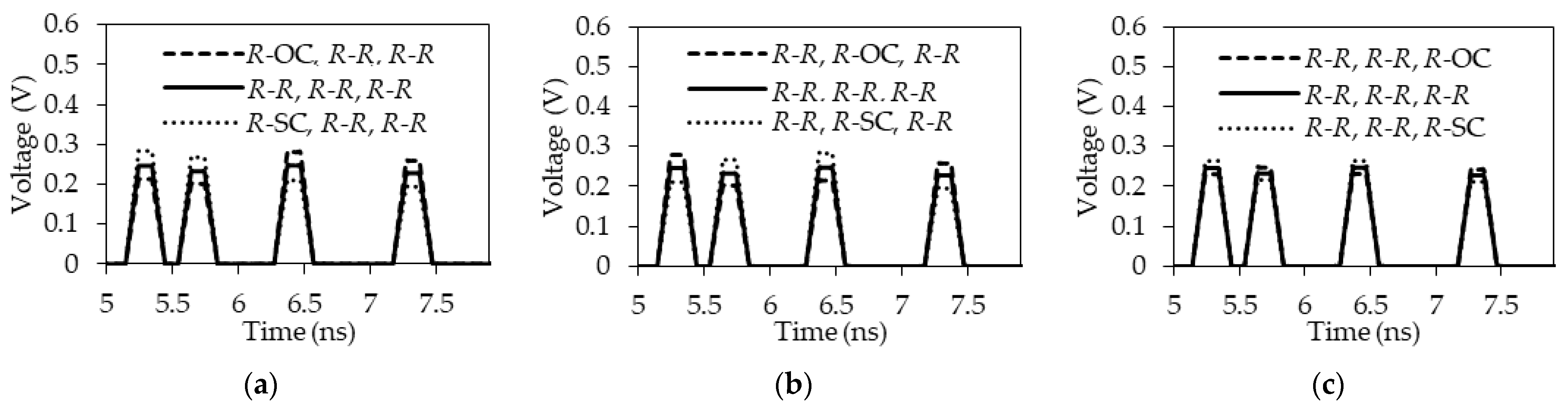
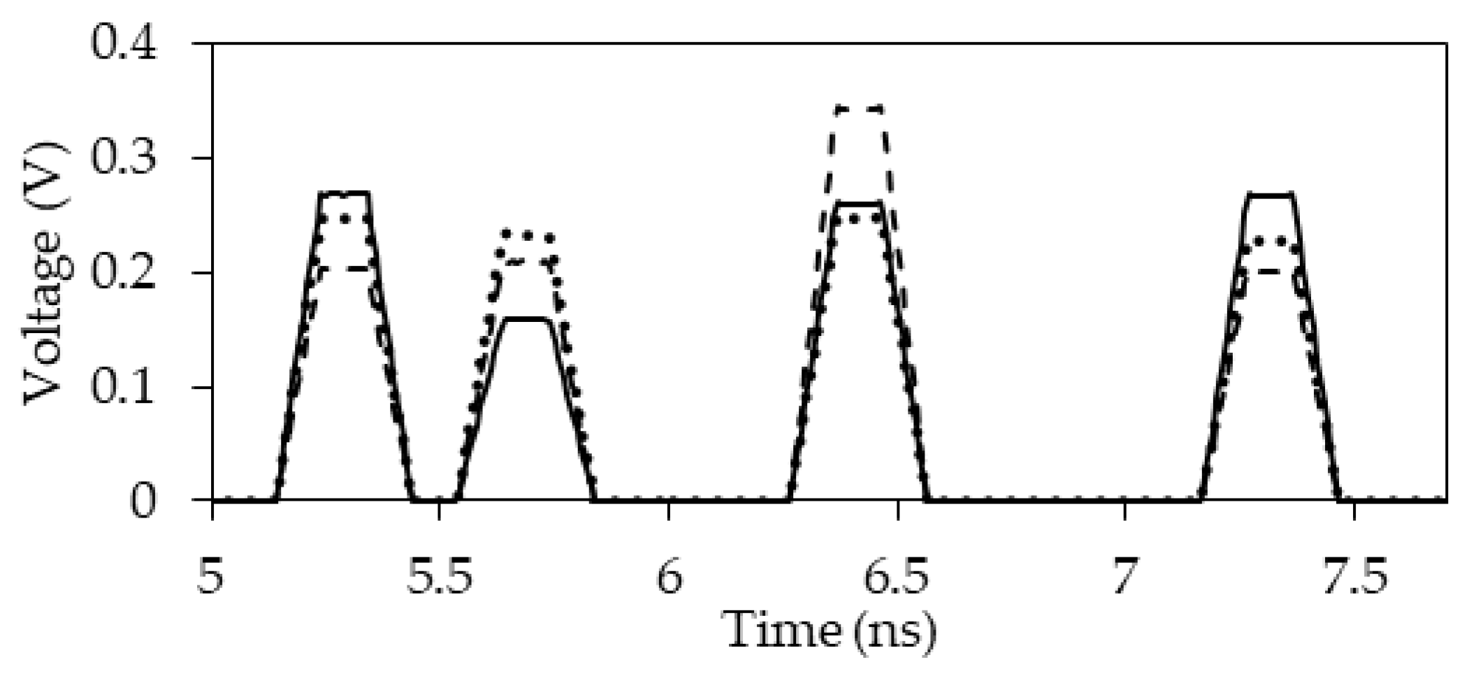
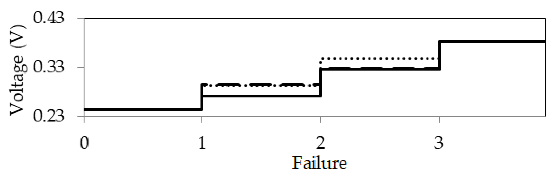
Figure 12.
Voltage waveforms at the far end of C1 under boundary conditions at the ends of passive conductors for R-R, R-R, R-R (∙∙∙∙), R-OC, OC-R, R-SC (––) и R-OC, SC-R, R-SC (---) (after failure 3).
Figure 12.
Voltage waveforms at the far end of C1 under boundary conditions at the ends of passive conductors for R-R, R-R, R-R (∙∙∙∙), R-OC, OC-R, R-SC (––) и R-OC, SC-R, R-SC (---) (after failure 3).
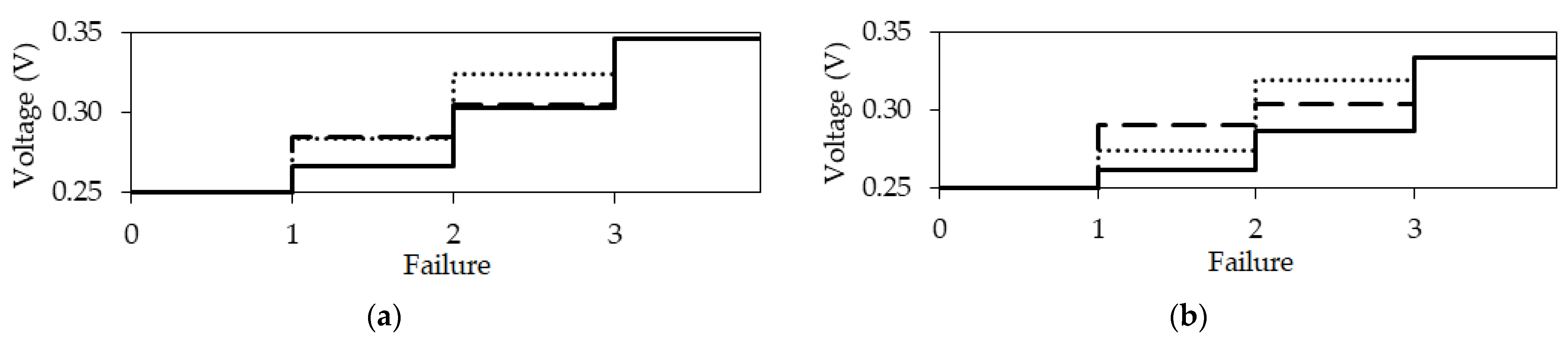
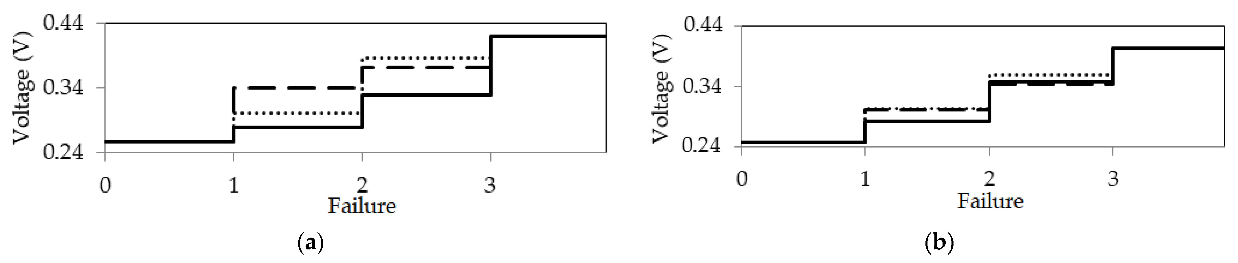
Figure 13.
Dependences of Umax values on the failure number with options 1 (∙∙∙), 2 (---), and 3 (––) for the structure with (a) original and (b) optimized parameter sets.
Figure 13.
Dependences of Umax values on the failure number with options 1 (∙∙∙), 2 (---), and 3 (––) for the structure with (a) original and (b) optimized parameter sets.
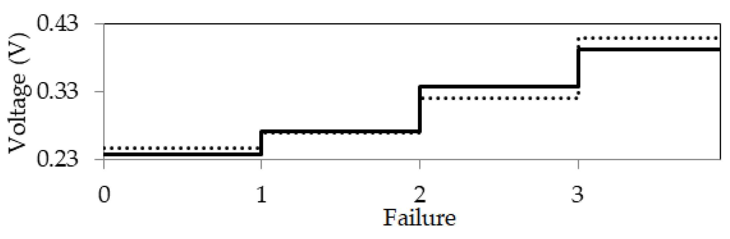
Figure 14.
Dependences of Umax values on the failure number at the optimal switching orders for the structure with the original (∙∙∙) and optimized (––) parameter sets.
Figure 14.
Dependences of Umax values on the failure number at the optimal switching orders for the structure with the original (∙∙∙) and optimized (––) parameter sets.
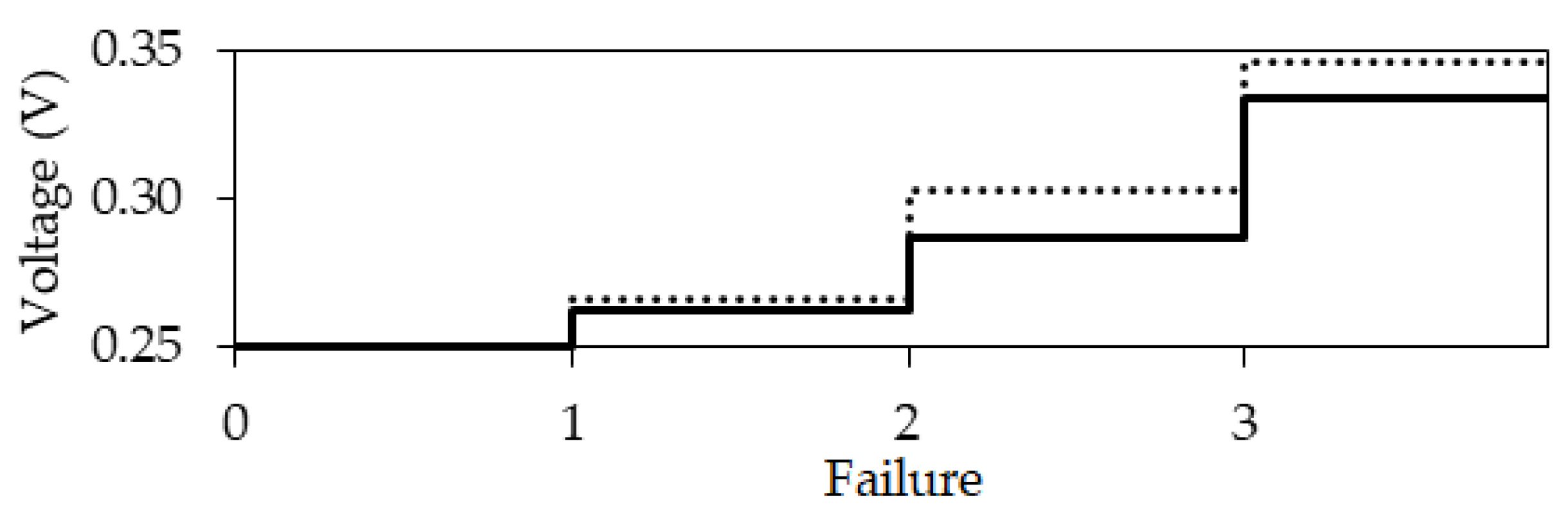
Figure 15.
Dependences of Umax values on the failure number at the switching options 1 (∙∙∙), 2 (---), and 3 (––) for the structure with the original parameter set.
Figure 15.
Dependences of Umax values on the failure number at the switching options 1 (∙∙∙), 2 (---), and 3 (––) for the structure with the original parameter set.
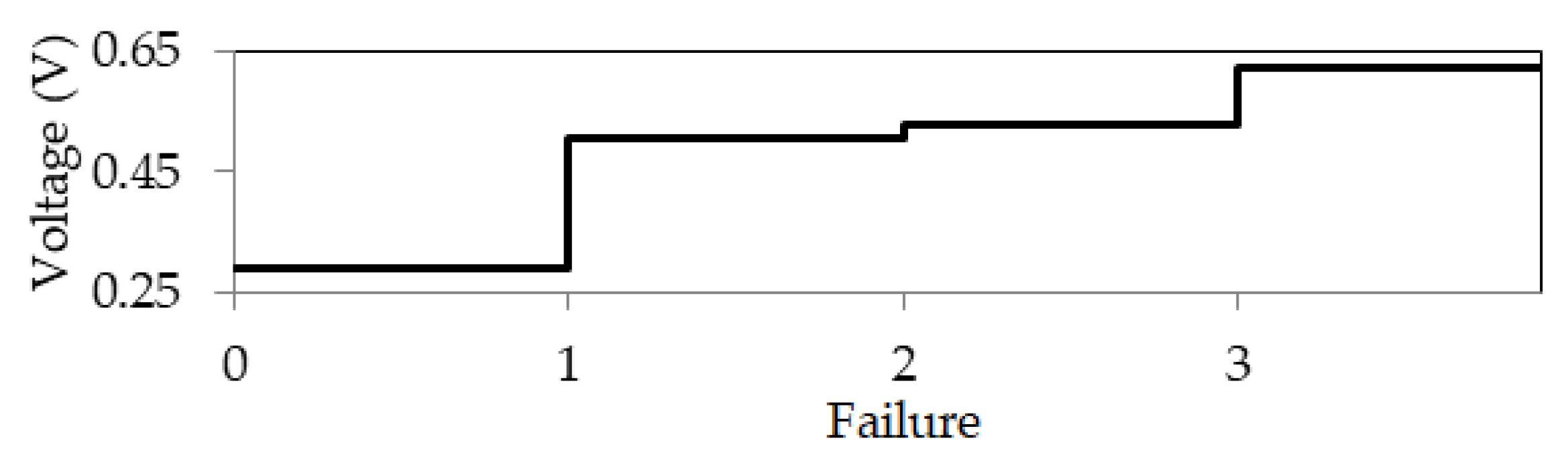
Figure 16.
Dependence of Umax for the optimal switching option from the failure number for a structure with an optimized parameter set.
Figure 16.
Dependence of Umax for the optimal switching option from the failure number for a structure with an optimized parameter set.
Figure 17.
Optimal switching order for active conductor after sequential failures at one of the ends of the active conductor for the structure with a triple MR with a reference conductor around.
Figure 17.
Optimal switching order for active conductor after sequential failures at one of the ends of the active conductor for the structure with a triple MR with a reference conductor around.
Figure 18.
Dependences of Umax values on the failure number for options 1, 2, and 3 for the structure with the original (∙∙∙) and optimized (––) parameter sets.
Figure 18.
Dependences of Umax values on the failure number for options 1, 2, and 3 for the structure with the original (∙∙∙) and optimized (––) parameter sets.
Figure 19.
Dependences of Umax for options 1 (∙∙∙), 2 (---), and 3 (––) on the number of failures in the structure with the original parameter set (a) 1, (b) 2, and (c) 3.
Figure 19.
Dependences of Umax for options 1 (∙∙∙), 2 (---), and 3 (––) on the number of failures in the structure with the original parameter set (a) 1, (b) 2, and (c) 3.
Figure 20.
Dependencies of Umax values for options 1 (∙∙∙), 2 (---), and 3 (––) on the failure number for the structure with the optimized parameter set.
Figure 20.
Dependencies of Umax values for options 1 (∙∙∙), 2 (---), and 3 (––) on the failure number for the structure with the optimized parameter set.
Figure 21.
Dependences of Umax values on the failure number for the structure with the original 1 (––), 2 (---), 3 (∙∙∙∙), and optimized (––) parameter sets.
Figure 21.
Dependences of Umax values on the failure number for the structure with the original 1 (––), 2 (---), 3 (∙∙∙∙), and optimized (––) parameter sets.
Figure 22.
Dependences of Umax on the failure number for options 1 (∙∙∙), 2 (---), and 3 (––) for the structure with (a) original and (b) optimized parameter sets.
Figure 22.
Dependences of Umax on the failure number for options 1 (∙∙∙), 2 (---), and 3 (––) for the structure with (a) original and (b) optimized parameter sets.
Figure 23.
Dependences of Umax values on the failure number for the structure with the original (∙∙∙) and optimized (––) parameter sets.
Figure 23.
Dependences of Umax values on the failure number for the structure with the original (∙∙∙) and optimized (––) parameter sets.
Table 1.
Cross-section parameter sets for strip structures.
Table 1.
Cross-section parameter sets for strip structures.
| Structure with a Reference Conductor | Parameter Sets | Parameter Values |
|---|
| s, μm | w, μm | t, μm | h, μm |
|---|
| In the center | 1 | 400 | 300 | 105 | 300 |
| 2 | 450 | 350 | 140 | 350 |
| 3 | 350 | 250 | 70 | 250 |
| Above and below | 1 | 200 | 200 | 35 | 180 |
| 2 | 250 | 250 | 70 | 200 |
| 3 | 150 | 150 | 18 | 150 |
| In the form of side polygons | 1 | 510 | 1600 | 35 | 500 |
| 2 | 550 | 1650 | 70 | 550 |
| 3 | 450 | 1550 | 18 | 450 |
Table 2.
Cross-section parameter set for shielded cable.
Table 2.
Cross-section parameter set for shielded cable.
| Structure with a Reference Conductor | Parameter Sets | Parameter Values |
|---|
| rc, μm | rd, μm | rr, μm |
|---|
| Around | 1 | 1500 | 1750 | 4350 |
| 2 | 2000 | 2250 | 5500 |
| 3 | 1000 | 1250 | 3100 |
Table 3.
Numerical characteristics of the structures under consideration after simulation.
Table 3.
Numerical characteristics of the structures under consideration after simulation.
| Structure with a Reference Conductor | Parameter Sets | Parameters |
|---|
| Umax, V | τ1, ns/m | τ2, ns/m | τ3, ns/m | τ4, ns/m | Δf, GHz | f1, GHz |
|---|
| In the center | 1 | 0.2473 | 2.544 | 2.735 | 3.082 | 3.573 | 0.296 | 1.436 |
| 2 | 0.2473 | 2.530 | 2.704 | 3.071 | 3.577 | 0.290 | 1.402 |
| 3 | 0.2471 | 2.564 | 2.780 | 3.099 | 3.567 | 0.302 | 1.482 |
| Around | 1 | 0.4970 | 5.475 | 5.475 | 5.780 | 6.370 | 0.337 | 1.666 |
| 2 | 0.4980 | 5.695 | 5.695 | 5.925 | 8.805 | 0.098 | 2.103 |
| 3 | 0.4960 | 5.785 | 5.785 | 6.020 | 7.705 | 0.158 | 1.861 |
| Above and below | 1 | 0.2490 | 3.582 | 4.185 | 4.430 | 4.585 | 0.340 | 1.596 |
| 2 | 0.2470 | 3.701 | 4.122 | 4.377 | 4.527 | 0.366 | 1.832 |
| 3 | 0.2510 | 3.720 | 4.230 | 4.460 | 4.635 | 0.344 | 1.692 |
| In the form of side polygons | 1 | 0.2437 | 2.239 | 2.453 | 2.936 | 3.201 | 0.286 | 0.662 |
| 2 | 0.2435 | 2.269 | 2.457 | 2.898 | 3.183 | 0.290 | 0.782 |
| 3 | 0.2435 | 2.207 | 2.445 | 2.961 | 3.217 | 0.282 | 0.696 |
Table 4.
Optimized parameters for strip structures.
Table 4.
Optimized parameters for strip structures.
| Structure with a Reference Conductor | s, μm | w, μm | h, μm | t, μm | d, μm |
|---|
| In the center | 510 | 1600 | 500 | 18 | 1600 |
| Above and below | 200 | 260 | 100 | 135 | 6400 |
| In the form of side polygons | 220 | 500 (w1 = 1600 μm) | 300 | 18 | 800 |
Table 5.
Parameter sets for simulation.
Table 5.
Parameter sets for simulation.
| Set | w, mm | s, mm | t, mm | h, mm | εr |
|---|
| Original | 0.3 | 0.40 | 0.105 | 0.3 | 5 |
| Optimized | 1.6 | 0.51 | 0.018 | 0.5 | 4.5 |
Table 6.
Umax values for optimal switching orders.
Table 6.
Umax values for optimal switching orders.
| Set | Before Failure | Umax, V | After Failure 1 | Umax, V | After Failure 2 | Umax, V | After Failure 3 | Umax, V |
|---|
| Original | R–R, R–R, R–R | 0.250 | R-R, R-R, R-SC | 0.266 | SC-R, R-R, R-SC | 0.303 | R-OC, SC-R, R-SC | 0.346 |
| Optimized | R–R, R–R, R–R | 0.250 | R-R, R-R, R-SC | 0.262 | SC-R, R-R, R-SC | 0.287 | R-SC, OC-R, SC-R | 0.334 |
Table 7.
Parameter sets for simulation.
Table 7.
Parameter sets for simulation.
| Set | rc, mm | rd, mm (Around Conductors) | rr, mm | εr (Around Conductors) |
|---|
| C1 | C2 | C3 | C4 | C1 | C2 | C3 | C4 | C1 | C2 | C3 | C4 |
|---|
| Original | 1.50 | 1.50 | 1.50 | 1.50 | 1.75 | 1.75 | 1.75 | 1.75 | 4.35 | 10 |
| Optimized | 0.90 | 0.80 | 0.80 | 0.70 | 0.97 | 0.95 | 0.95 | 0.95 | 3.50 | 30 | 5 | 16 | 6 |
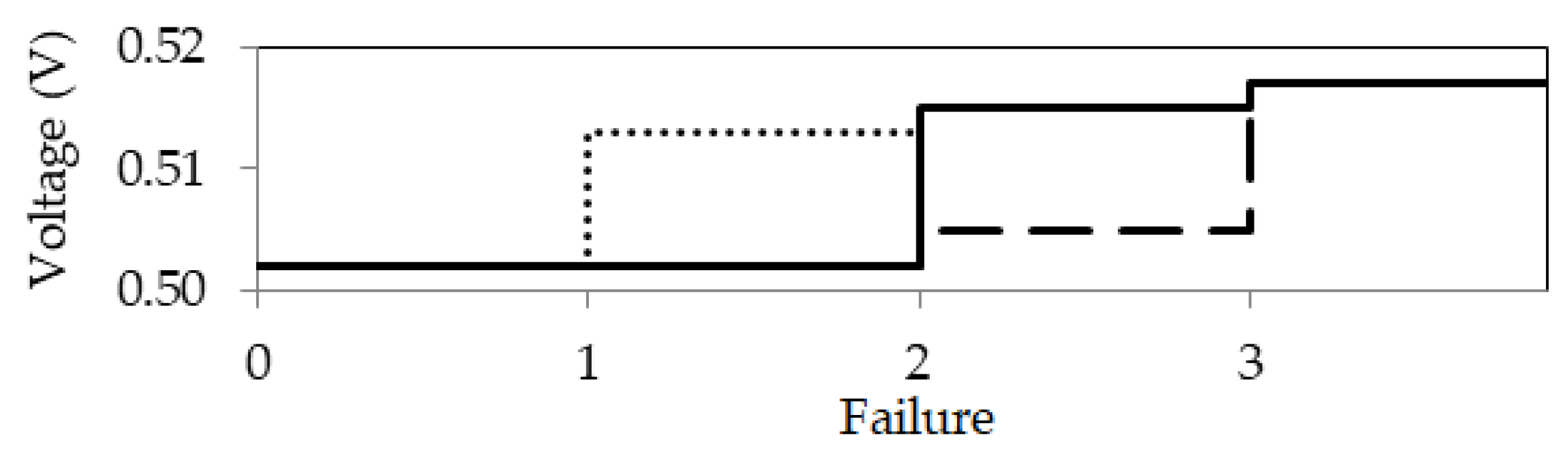
Table 8.
Umax values for optimal switching orders.
Table 8.
Umax values for optimal switching orders.
| Set | Before Failure | Umax, V | After Failure 1 | Umax, V | After Failure 2 | Umax, V | After Failure 3 | Umax, V |
|---|
| Original | R–R, R–R, R–R | 0.502 | R-R, R-R, R-OC | 0.502 | R-R, R-SC, OC-R | 0.505 | R-OC, R-SC, R-SC | 0.517 |
| Optimized | R–R, R–R, R–R | 0.291 | R-R, R-R, R-SC | 0.507 | R-SC, R-R, SC-R | 0.527 | R-OC, R-SC, SC-R | 0.622 |
Table 9.
Parameter sets for simulation.
Table 9.
Parameter sets for simulation.
| Set | w, mm | s, mm | t, mm | h, mm | h1, mm | εr | εr1 |
|---|
| 1 | 0.200 | 0.200 | 0.035 | 0.137 | 0.250 | 10.2 | 4.3 |
| 2 | 0.200 | 0.200 | 0.035 | 0.206 | 0.360 | 10.2 | 4.3 |
| 3 | 0.200 | 0.200 | 0.035 | 0.360 | 0.360 | 10.2 | 4.3 |
| Optimized | 0.260 | 0.200 | 0.135 | 0.200 | 0.400 | 10.2 | 4.3 |
Table 10.
Umax values for optimal switching orders.
Table 10.
Umax values for optimal switching orders.
| Set | Before Failure | Umax, V | After Failure 1 | Umax, V | After Failure 2 | Umax, V | After Failure 3 | Umax, V |
|---|
| 1 | R-R, R-R, R-R | 0.248 | R-R, R-R, R-SC | 0.266 | SC-R, R-R, R-SC | 0.289 | R-SC, OC-R, SC-R | 0.361 |
| 2 | R-R, R-R, R-R | 0.252 | R-R, R-R, R-SC | 0.274 | SC-R, R-R, R-SC | 0.309 | R-SC, OC-R, SC-R | 0.373 |
| 3 | R-R, R-R, R-R | 0.250 | R-R, R-R, R-SC | 0.269 | SC-R, R-R, R-SC | 0.308 | R-SC, OC-R, SC-R | 0.352 |
| Optimized | R-R, R-R, R-R | 0.243 | R-R, R-R, R-SC | 0.271 | SC-R, R-R, R-SC | 0.327 | R-SC, OC-R, SC-R | 0.383 |
Table 11.
Parameter sets for simulation.
Table 11.
Parameter sets for simulation.
| Set | w, mm | w1, mm | s, mm | t, mm | h, mm | εr | d, mm |
|---|
| Original | 1.6 | 1.6 | 0.51 | 0.018 | 0.5 | 4.5 | 1.6 |
| Optimized | 0.5 | 1.6 | 0.22 | 0.018 | 0.3 | 4.5 | 8 |
Table 12.
Umax values for optimal switching orders.
Table 12.
Umax values for optimal switching orders.
| Set | Before Failure | Umax, V | After Failure 1 | Umax, V | After Failure 2 | Umax, V | After Failure 3 | Umax, V |
|---|
| Original | R–R, R–R, R–R | 0.247 | R-R, R-R, R-SC | 0.270 | OC-R, R-R, R-SC | 0.320 | R-SC, OC-R, SC-R | 0.409 |
| Optimized | R–R, R–R, R–R | 0.237 | R-R, R-R, R-SC | 0.272 | SC-R, R-R, R-SC | 0.337 | R-SC, OC-R, SC-R | 0.393 |


 ,
, 


