GaAs Nanowires Grown by Catalyst Epitaxy for High Performance Photovoltaics

 , ,
, ,
Abstract
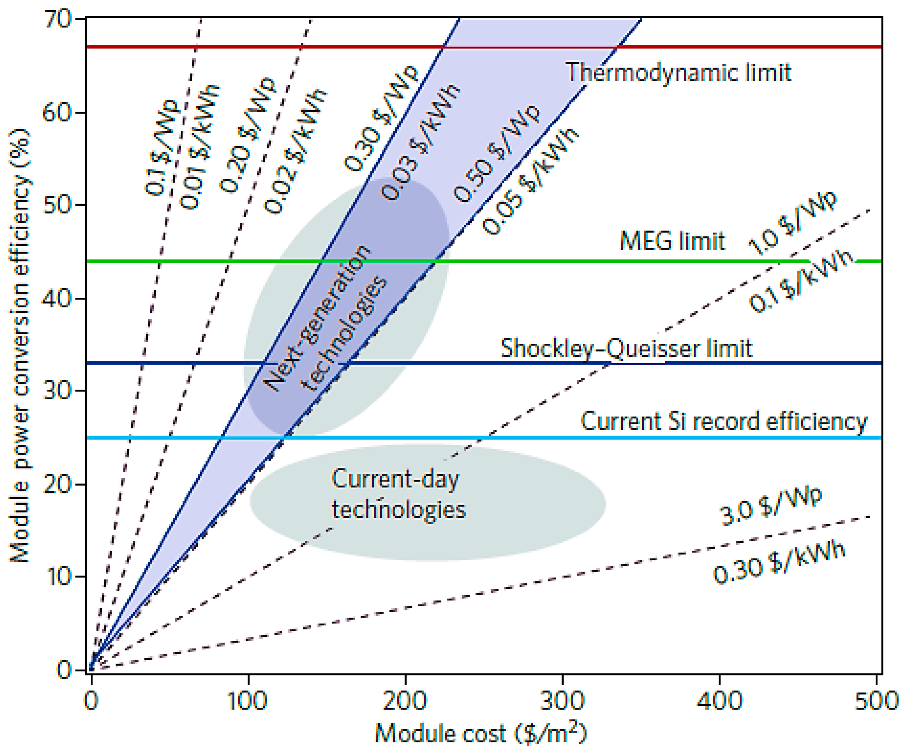
:1. Introduction
2. GaAs NW Growth via Catalyst Epitaxy
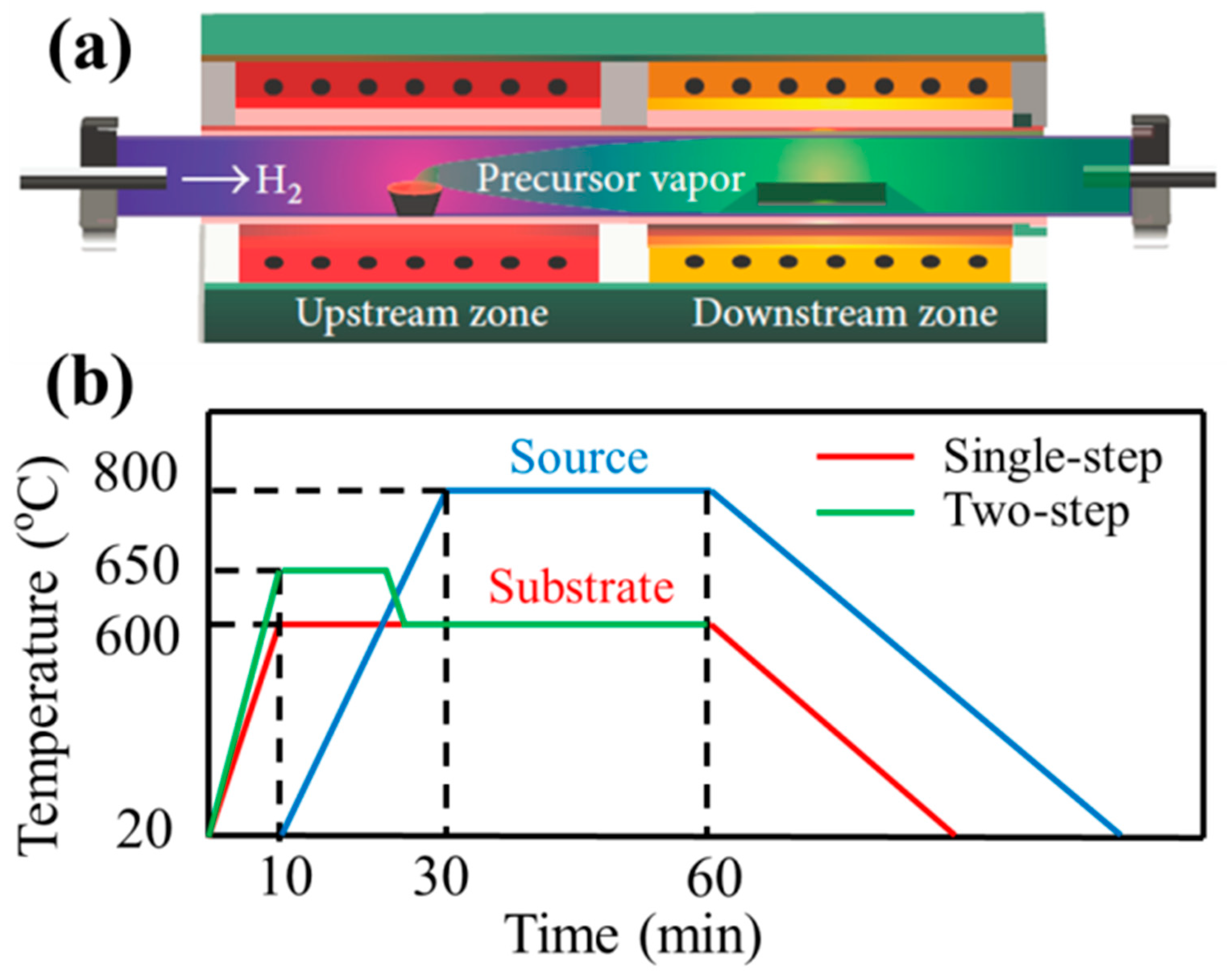
2.1. The VLS and VSS Growth Methods
2.2. GaAs NW Growth via Catalyst Epitaxy
2.3. Evaluations of the Catalyst Epitaxy
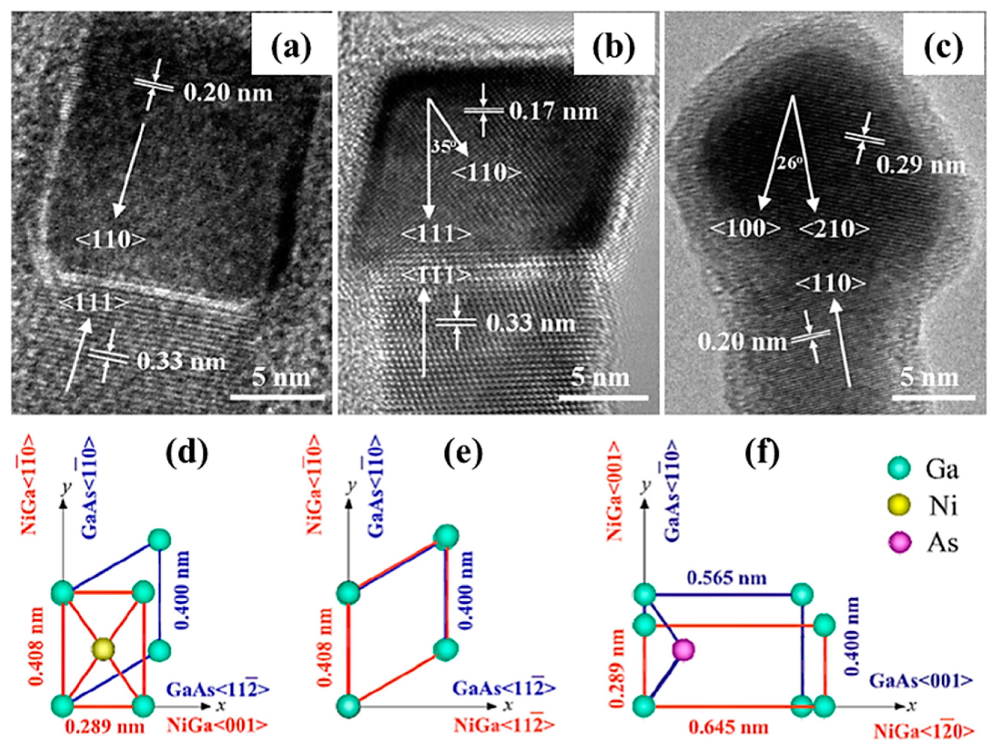
2.4. Catalyst Engineering for Tuned Growth of GaAs NW
3. The Structure-Property Relationships
4. Optical Absorption
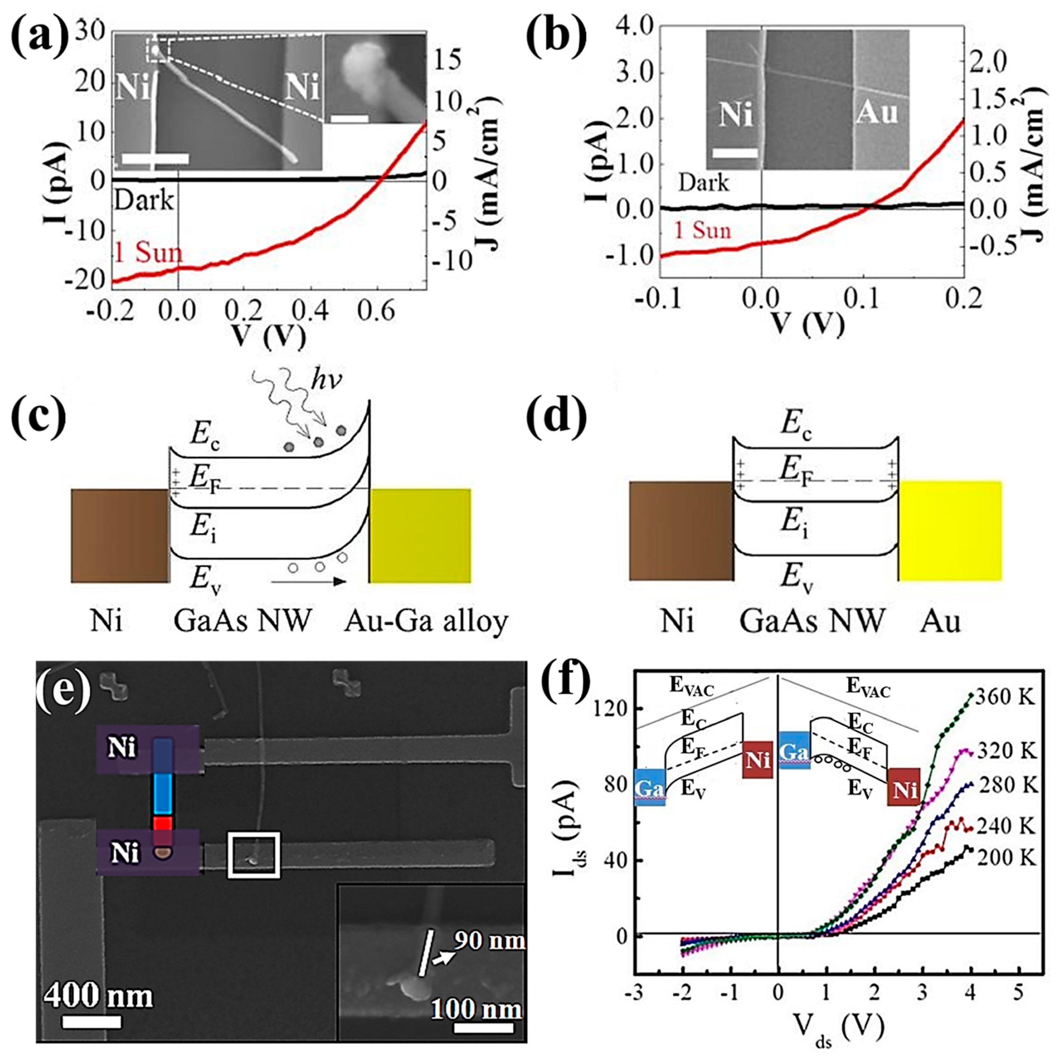
5. PV Device Fabrication and Performances
6. Conclusions and Remarks
Author Contributions
Funding
Acknowledgments
Conflicts of Interest
References
- Lohse, C. Environmental impact by hydrogeothermal energy generation in low-enthalpy regions. Renew. Energy 2018, 128, 509–519. [Google Scholar] [CrossRef]
- Cao, X.H.; Tan, C.L.; Zhang, X.; Zhao, W.; Zhang, H. Solution-processed two-dimensional metal dichalcogenide-based nanomaterials for energy storage and conversion. Adv. Mater. 2016, 28, 6167–6196. [Google Scholar] [CrossRef] [PubMed]
- Chu, S.; Majumdar, A. Opportunities and challenges for a sustainable energy future. Nature 2012, 488, 294–303. [Google Scholar] [CrossRef] [PubMed]
- Lewis, N.S. Toward cost-effective solar energy use. Science 2007, 315, 798–801. [Google Scholar] [CrossRef] [PubMed]
- Petrov, O.; Bi, X.T.; Lau, A. Impact assessment of biomass-based district heating systems in densely populated communities. Part II: Would the replacement of fossil fuels improve ambient air quality and human health? Atmos. Environ. 2017, 161, 191–199. [Google Scholar] [CrossRef]
- Hidy, G.M. Multiscale impact of fuel consumption on air quality. Energy Fuels 2002, 16, 270–281. [Google Scholar] [CrossRef]
- Poizot, P.; Dolhem, F. Clean energy new deal for a sustainable world: From non-CO2 generating energy sources to greener electrochemical storage devices. Energy Environ. Sci. 2011, 4, 2003–2019. [Google Scholar] [CrossRef]
- Zhou, H.L.; Qu, Y.Q.; Zeid, T.; Duan, X.F. Towards highly efficient photocatalysts using semiconductor nanoarchitectures. Energy Environ. Sci. 2012, 5, 6732–6743. [Google Scholar] [CrossRef]
- Chen, J.; Huang, Y.; Zhang, N.N.; Zou, H.Y.; Liu, R.Y.; Tao, C.Y.; Fan, X.; Wang, Z.L. Micro-cable structured textile for simultaneously harvesting solar and mechanical energy. Nat. Energy 2016, 1, 16138. [Google Scholar] [CrossRef]
- Han, N.; Yang, Z.X.; Shen, L.F.; Lin, H.; Wang, Y.; Pun, E.Y.B.; Chen, Y.F.; Ho, J.C. Design and fabrication of 1-D semiconductor nanomaterials for high-performance photovoltaics. Sci. Bull. 2016, 61, 357–367. [Google Scholar] [CrossRef]
- LaPierre, R.R.; Chia, A.C.E.; Gibson, S.J.; Haapamaki, C.M.; Boulanger, J.; Yee, R.; Kuyanov, P.; Zhang, J.; Tajik, N.; Jewell, N.; et al. III-V nanowire photovoltaics: Review of design for high efficiency. Phys. Status Solidi-R. 2013, 7, 815–830. [Google Scholar] [CrossRef] [Green Version]
- Beard, M.C.; Luther, J.M.; Nozik, A.J. The promise and challenge of nanostructured solar cells. Nat. Nanotechnol. 2014, 9, 951–954. [Google Scholar] [CrossRef] [PubMed]
- Beard, M.C.; Luther, J.M.; Semonin, O.E.; Nozik, A.J. Third generation photovoltaics based on multiple exciton generation in quantum confined semiconductors. Acc. Chem. Res. 2013, 46, 1252–1260. [Google Scholar] [CrossRef] [PubMed]
- Green, M.A. The path to 25% silicon solar cell efficiency: History of silicon cell evolution. Prog. Photovolt. 2009, 17, 183–189. [Google Scholar] [CrossRef] [Green Version]
- Polman, A.; Atwater, H.A. Photonic design principles for ultrahigh-efficiency photovoltaics. Nat. Mater. 2012, 11, 174–177. [Google Scholar] [CrossRef] [PubMed]
- Conibeer, G. Third-generation photovoltaics. Mater. Today 2007, 10, 42–50. [Google Scholar] [CrossRef]
- Cao, F.; Chen, K.X.; Zhang, J.J.; Ye, X.Y.; Li, J.J.; Zou, S.; Su, X.D. Next-generation multi-crystalline silicon solar cells: Diamond-wire sawing, nano-texture and high efficiency. Sol. Energy Mater. Sol. C 2015, 141, 132–138. [Google Scholar] [CrossRef]
- Placzek-Popko, E. Top PV market solar cells 2016. Opto-Electron. Rev. 2017, 25, 55–64. [Google Scholar] [CrossRef]
- Spinelli, P.; Ferry, V.E.; van de Groep, J.; van Lare, M.; Verschuuren, M.A.; Schropp, R.E.I.; Atwater, H.A.; Polman, A. Plasmonic light trapping in thin-film Si solar cells. J. Opt. 2012, 14, 024002. [Google Scholar] [CrossRef]
- Lee, T.D.; Ebong, A.U. A review of thin film solar cell technologies and challenges. Renew. Sustain. Energy Rev. 2017, 70, 1286–1297. [Google Scholar] [CrossRef]
- Gowrishankar, V.; Luscombe, C.K.; McGehee, M.D.; Frechet, J.M.J. High-efficiency, Cd-free copper-indium-gallium-diselenide/polymer hybrid solar cells. Sol. Energy Mater. Sol. C 2007, 91, 807–812. [Google Scholar] [CrossRef]
- Bhattacharya, R.N. CIGS-based solar cells prepared from electrodeposited stacked Cu/In/Ga layers. Sol. Energy Mater. Sol. C 2013, 113, 96–99. [Google Scholar] [CrossRef]
- Avrutin, V.; Izyumskaya, N.; Morkoc, H. Semiconductor solar cells: Recent progress in terrestrial applications. Superlattices Microstruct. 2011, 49, 337–364. [Google Scholar] [CrossRef]
- Greenaway, A.L.; Boucher, J.W.; Oener, S.Z.; Funch, C.J.; Boettcher, S.W. Low-Cost Approaches to III-V Semiconductor Growth for Photovoltaic Applications. ACS Energy Lett. 2017, 2, 2270–2282. [Google Scholar] [CrossRef]
- Shockley, W.; Queisser, H.J. Detailed balance limit of efficiency of p-n junction solar cells. J. Appl. Phys. 1961, 32, 510–519. [Google Scholar] [CrossRef]
- Green, M.A. Analytical treatment of Trivich-Flinn and Shockley-Queisser photovoltaic efficiency limits using polylogarithms. Prog. Photovolt. 2012, 20, 127–134. [Google Scholar] [CrossRef]
- Mann, S.A.; Grote, R.R.; Osgood, R.M.; Alu, A.; Garneet, E.C. Opportunities and Limitations for Nanophotonic Structures to Exceed the Shockley-Queisser Limit. ACS Nano 2016, 10, 8620–8631. [Google Scholar] [CrossRef] [PubMed]
- Yu, Z.F.; Sandhu, S.; Fan, S.H. Efficiency above the Shockley-Queisser Limit by using nanophotonic effects to create multiple effective bandgaps with a single semiconductor. Nano Lett. 2014, 14, 66–70. [Google Scholar] [CrossRef] [PubMed]
- Rao, A.; Friend, R.H. Harnessing singlet exciton fission to break the Shockley-Queisser limit. Nat. Rev. Mater. 2017, 2, 17063. [Google Scholar] [CrossRef]
- Brown, G.F.; Wu, J.Q. Third generation photovoltaics. Laser Photonics Rev. 2009, 3, 394–405. [Google Scholar] [CrossRef]
- Anttu, N. Shockley-Queisser Detailed Balance Efficiency Limit for Nanowire Solar Cells. ACS Photonics 2015, 2, 446–453. [Google Scholar] [CrossRef]
- Davis, N.; Bohm, M.L.; Tabachnyk, M.; Wisnivesky-Rocca-Rivarola, F.; Jellicoe, T.C.; Ducati, C.; Ehrler, B.; Greenham, N.C. Multiple-exciton generation in lead selenide nanorod solar cells with external quantum efficiencies exceeding 120%. Nat. Commun. 2015, 6, 8259. [Google Scholar] [CrossRef] [PubMed] [Green Version]
- Devos, A. Detailed balance limit of the efficiency of tandem solar-cells. J. Phys. D Appl. Phys. 1980, 13, 839–846. [Google Scholar]
- Choi, J.J.; Wenger, W.N.; Hoffman, R.S.; Lim, Y.-F.; Luria, J.; Jasieniak, J.; Marohn, J.A.; Hanrath, T. Solution-processed nanocrystal quantum dot tandem solar cells. Adv. Mater. 2011, 23, 3144–3148. [Google Scholar] [CrossRef] [PubMed]
- Wang, X.; Koleilat, G.I.; Tang, J.; Liu, H.; Kramer, I.J.; Debnath, R.; Brzozowski, L.; Barkhouse, D.A.R.; Levina, L.; Hoogland, S.; et al. Tandem colloidal quantum dot solar cells employing a graded recombination layer. Nat. Photonics 2011, 5, 480–484. [Google Scholar] [CrossRef]
- Green, M.A.; Emery, K.; Hishikawa, Y.; Warta, W.; Dunlop, E.D. Solar cell efficiency tables (version 44). Prog. Photovolt. 2014, 22, 701–710. [Google Scholar] [CrossRef] [Green Version]
- Xue, Q.F.; Xia, R.X.; Brabec, C.J.; Yip, H.L. Recent advances in semi-transparent polymer and perovskite solar cells for power generating window applications. Energy Environ. Sci. 2018, 11, 1688–1709. [Google Scholar] [CrossRef]
- Zhao, B.D.; Abdi-Jalebi, M.; Tabachnyk, M.; Glass, H.; Kamboj, V.S.; Nie, W.Y.; Pearson, A.J.; Puttisong, Y.; Godel, K.C.; Beere, H.E.; et al. High open-circuit voltages in tin-rich low-bandgap perovskite-based planar heterojunction photovoltaics. Adv. Mater. 2017, 29, 1604744. [Google Scholar] [CrossRef] [PubMed]
- Nozik, A.J. Spectroscopy and hot electron relaxation dynamics in semiconductor quantum wells and quantum dots. Annu. Rev. Phys. Chem. 2001, 52, 193–231. [Google Scholar] [CrossRef] [PubMed]
- Beard, M.C.; Midgett, A.G.; Law, M.; Semonin, O.E.; Ellingson, R.J.; Nozik, A.J. Variations in the quantum efficiency of multiple exciton generation for a series of chemically treated pbse nanocrystal films. Nano Lett. 2009, 9, 836–845. [Google Scholar] [CrossRef] [PubMed]
- Cirloganu, C.M.; Padilha, L.A.; Lin, Q.; Makarov, N.S.; Velizhanin, K.A.; Luo, H.; Robel, I.; Pietryga, J.M.; Klimov, V.I. Enhanced carrier multiplication in engineered quasi-type-II quantum dots. Nat. Commun. 2014, 5, 4148. [Google Scholar] [CrossRef] [PubMed]
- Nozik, A.J. Quantum dot solar cells. Phys. E Low Dimens. Syst. Nanostruct. 2002, 14, 115–120. [Google Scholar] [CrossRef]
- Jia, Y.; Wei, J.Q.; Wang, K.L.; Cao, A.Y.; Shu, Q.K.; Gui, X.C.; Zhu, Y.Q.; Zhuang, D.M.; Zhang, G.; Ma, B.B.; et al. Nanotube-silicon heterojunction solar cells. Adv. Mater. 2008, 20, 4594–4598. [Google Scholar] [CrossRef]
- Chen, T.; Wang, S.T.; Yang, Z.B.; Feng, Q.Y.; Sun, X.M.; Li, L.; Wang, Z.S.; Peng, H.S. Flexible, light-weight, ultrastrong, and semiconductive carbon nanotube fibers for a highly efficient solar cell. Angew. Chem. Int. Ed. 2011, 50, 1815–1819. [Google Scholar] [CrossRef] [PubMed]
- Mir, N.; Lee, K.; Paramasivam, I.; Schmuki, P. Optimizing TiO2 nanotube top geometry for use in dye-sensitized solar cells. Chem. Eur. J. 2012, 18, 11862–11866. [Google Scholar] [CrossRef] [PubMed]
- Liu, J.; Yi, F.T.; Wang, B.; Zhang, T.C.; Wang, Y.T.; Zhou, Y. Fabrication and photovoltaic effect of cds/silicon nanopillars heterojunction solar cell. ChemistrySelect 2016, 1, 4901–4905. [Google Scholar] [CrossRef]
- Sealy, C. Nanopillars could spell cheaper, more efficient solar cells. Nano Today 2009, 4, 379. [Google Scholar]
- Sun, H.; Ren, F.; Ng, K.W.; Tran, T.T.D.; Li, K.; Chang-Hasnain, C.J. Nanopillar lasers directly grown on silicon with heterostructure surface passivation. ACS Nano 2014, 8, 6833–6839. [Google Scholar] [CrossRef] [PubMed]
- Baxter, J.B.; Aydil, E.S. Nanowire-based dye-sensitized solar cells. Appl. Phys. Lett. 2005, 86, 053114. [Google Scholar] [CrossRef]
- Tsakalakos, L.; Balch, J.; Fronheiser, J.; Korevaar, B.A.; Sulima, O.; Rand, J. Silicon nanowire solar cells. Appl. Phys. Lett. 2007, 91, 233117. [Google Scholar] [CrossRef]
- Garnett, E.C.; Yang, P. Silicon nanowire radial p-n junction solar cells. J. Am. Chem. Soc. 2008, 130, 9224–9225. [Google Scholar] [CrossRef] [PubMed]
- Garnett, E.; Yang, P. Light trapping in silicon nanowire solar cells. Nano Lett. 2010, 10, 1082–1087. [Google Scholar] [CrossRef] [PubMed]
- Kelzenberg, M.D.; Boettcher, S.W.; Petykiewicz, J.A.; Turner-Evans, D.B.; Putnam, M.C.; Warren, E.L.; Spurgeon, J.M.; Briggs, R.M.; Lewis, N.S.; Atwater, H.A. Enhanced absorption and carrier collection in Si wire arrays for photovoltaic applications. Nat. Mater. 2010, 9, 239–244. [Google Scholar] [CrossRef] [PubMed]
- Borgstrom, M.T.; Wallentin, J.; Heurlin, M.; Falt, S.; Wickert, P.; Leene, J.; Magnusson, M.H.; Deppert, K.; Samuelson, L. Nanowires with promise for photovoltaics. IEEE J. Sel. Top. Quantum Electron. 2011, 17, 1050–1061. [Google Scholar] [CrossRef]
- Peng, K.-Q.; Lee, S.-T. Silicon nanowires for photovoltaic solar energy conversion. Adv. Mater. 2011, 23, 198–215. [Google Scholar] [CrossRef] [PubMed]
- Wang, Y.; Yang, Z.X.; Wu, X.F.; Han, N.; Liu, H.Y.; Wang, S.B.; Li, J.; Tse, W.; Yip, S.; Chen, Y.F.; et al. Growth and photovoltaic properties of high-quality gaas nanowires prepared by the two-source CVD method. Nanoscale Res. Lett. 2016, 11, 191. [Google Scholar] [CrossRef] [PubMed]
- Yoon, J.; Jo, S.; Chun, I.S.; Jung, I.; Kim, H.-S.; Meitl, M.; Menard, E.; Li, X.; Coleman, J.J.; Paik, U.; et al. GaAs photovoltaics and optoelectronics using releasable multilayer epitaxial assemblies. Nature 2010, 465, 329. [Google Scholar] [CrossRef] [PubMed]
- Han, N.; Wang, F.; Yip, S.; Hou, J.J.; Xiu, F.; Shi, X.; Hui, A.T.; Hung, T.; Ho, J.C. GaAs nanowire Schottky barrier photovoltaics utilizing Au-Ga alloy catalytic tips. Appl. Phys. Lett. 2012, 101, 013105. [Google Scholar] [CrossRef]
- Otnes, G.; Borgstrom, M.T. Towards high efficiency nanowire solar cells. Nano Today 2017, 12, 31–45. [Google Scholar] [CrossRef]
- Yao, M.; Huang, N.; Cong, S.; Chi, C.-Y.; Seyedi, M.A.; Lin, Y.-T.; Cao, Y.; Povinelli, M.L.; Dapkus, P.D.; Zhou, C. GaAs Nanowire array solar cells with axial p-i-n junctions. Nano Lett. 2014, 14, 3293–3303. [Google Scholar] [CrossRef] [PubMed]
- Afshar, E.N.; Xosrovashvili, G.; Rouhi, R.; Gorji, N.E. Review on the application of nanostructure materials in solar cells. Mod. Phys. Lett. B 2015, 29, 1550118. [Google Scholar] [CrossRef]
- Aberg, I.; Vescovi, G.; Asoli, D.; Naseem, U.; Gilboy, J.P.; Sundvall, C.; Dahlgren, A.; Svensson, K.E.; Anttu, N.; Bjork, M.T.; et al. A GaAs nanowire array solar cell with 15.3% efficiency at 1 sun. IEEE J. Photovolt. 2016, 6, 185–190. [Google Scholar] [CrossRef]
- Yu, S.; Witzigmann, B. A high efficiency dual-junction solar cell implemented as a nanowire array. Opt. Express 2013, 21, A167–A172. [Google Scholar] [CrossRef] [PubMed]
- Im, J.-H.; Luo, J.; Franckevicius, M.; Pellet, N.; Gao, P.; Moehl, T.; Zakeeruddin, S.M.; Nazeeruddin, M.K.; Graetzel, M.; Park, N.-G. Nanowire perovskite solar cell. Nano Lett. 2015, 15, 2120–2126. [Google Scholar] [CrossRef] [PubMed]
- Wang, Y.; Zhang, Y.; Zhang, D.; He, S.; Li, X. Design high-efficiency III-V nanowire/Si two-junction solar cell. Nanoscale Res. Lett. 2015, 10, 269. [Google Scholar] [CrossRef] [PubMed]
- Wu, S.-H.; Povinelli, M.L. Solar heating of GaAs nanowire solar cells. Opt. Express 2015, 23, A1363–A1372. [Google Scholar] [CrossRef] [PubMed]
- Boulanger, J.P.; Chia, A.C.E.; Wood, B.; Yazdi, S.; Kasama, T.; Aagesen, M.; LaPierre, R.R. Characterization of a Ga-Assisted GaAs Nanowire Array Solar Cell on Si Substrate. IEEE J. Photovolt. 2016, 6, 661–667. [Google Scholar] [CrossRef]
- Luo, Y.B.; Yan, X.; Zhang, J.N.; Li, B.; Wu, Y.; Lu, Q.C.; Jin, C.X.S.; Zhang, X.; Ren, X.M. A graphene/single GaAs nanowire Schottky junction photovoltaic device. Nanoscale 2018, 10, 9212–9217. [Google Scholar] [CrossRef] [PubMed]
- Wallentin, J.; Anttu, N.; Asoli, D.; Huffman, M.; Aberg, I.; Magnusson, M.H.; Siefer, G.; Fuss-Kailuweit, P.; Dimroth, F.; Witzigmann, B.; et al. InP nanowire array solar cells achieving 13.8% efficiency by exceeding the ray optics limit. Science 2013, 339, 1057–1060. [Google Scholar] [CrossRef] [PubMed]
- Yao, M.; Cong, S.; Arab, S.; Huang, N.; Povinelli, M.L.; Cronin, S.B.; Dapkus, P.D.; Zhou, C. Tandem solar cells using gaas nanowires on Si: Design, fabrication, and observation of voltage addition. Nano Lett. 2015, 15, 7217–7224. [Google Scholar] [CrossRef] [PubMed]
- Atwater, H.A.; Polman, A. Plasmonics for improved photovoltaic devices. Nat. Mater. 2010, 9, 205–213. [Google Scholar] [CrossRef] [PubMed]
- Kempa, T.J.; Cahoon, J.F.; Kim, S.-K.; Day, R.W.; Bell, D.C.; Park, H.-G.; Lieber, C.M. Coaxial multishell nanowires with high-quality electronic interfaces and tunable optical cavities for ultrathin photovoltaics. Proc. Natl. Acad. Sci. USA 2012, 109, 1407–1412. [Google Scholar] [CrossRef] [PubMed] [Green Version]
- Heiss, M.; Morral, A.F.I. Fundamental limits in the external quantum efficiency of single nanowire solar cells. Appl. Phys. Lett. 2011, 99, 263102. [Google Scholar] [CrossRef] [Green Version]
- Krogstrup, P.; Jorgensen, H.I.; Heiss, M.; Demichel, O.; Holm, J.V.; Aagesen, M.; Nygard, J.; Morral, A.F.I. Single-nanowire solar cells beyond the Shockley-Queisser limit. Nat. Photonics 2013, 7, 306–310. [Google Scholar] [CrossRef]
- Mariani, G.; Wong, P.S.; Katzenmeyer, A.M.; Leonard, F.; Shapiro, J.; Huffaker, D.L. Patterned radial GaAs nanopillar solar cells. Nano Lett. 2011, 11, 2490–2494. [Google Scholar] [CrossRef] [PubMed]
- Holm, J.V.; Jorgensen, H.I.; Krogstrup, P.; Nygard, J.; Liu, H.; Aagesen, M. Surface-passivated GaAsP single-nanowire solar cells exceeding 10% efficiency grown on silicon. Nat. Commun. 2013, 4, 1498. [Google Scholar] [CrossRef] [PubMed] [Green Version]
- Mariani, G.; Scofield, A.C.; Hung, C.H.; Huffaker, D.L. GaAs nanopillar-array solar cells employing in situ surface passivation. Nat. Commun. 2013, 4, 1497. [Google Scholar] [CrossRef] [PubMed] [Green Version]
- Colombo, C.; Heiss, M.; Graetzel, M.; Fontcuberta i Morral, A. Gallium arsenide p-i-n radial structures for photovoltaic applications. Appl. Phys. Lett. 2009, 94, 173108. [Google Scholar] [CrossRef] [Green Version]
- Schubert, M.B.; Werner, J.H. Flexible solar cells for clothing. Mater. Today 2006, 9, 42–50. [Google Scholar] [CrossRef]
- Fan, Z.; Razavi, H.; Do, J.-W.; Moriwaki, A.; Ergen, O.; Chueh, Y.-L.; Leu, P.W.; Ho, J.C.; Takahashi, T.; Reichertz, L.A.; et al. Three-dimensional nanopillar-array photovoltaics on low-cost and flexible substrates. Nat. Mater. 2009, 8, 648–653. [Google Scholar] [CrossRef] [PubMed]
- Han, N.; Yang, Z.-X.; Wang, F.; Dong, G.; Yip, S.; Liang, X.; Hung, T.F.; Chen, Y.; Ho, J.C. High-performance GaAs nanowire solar cells for flexible and transparent photovoltaics. ACS Appl. Mater. Interfaces 2015, 7, 20454–20459. [Google Scholar] [CrossRef] [PubMed]
- Wang, X.Y.; Du, W.N.; Yang, X.G.; Zhang, X.W.; Yang, T. Self-catalyzed growth mechanism of InAs nanowires and growth of InAs/GaSb heterostructured nanowires on Si substrates. J. Cryst. Growth 2015, 426, 287–292. [Google Scholar] [CrossRef]
- Schroth, P.; Jakob, J.; Feigl, L.; Kashani, S.M.M.; Vogel, J.; Strempfer, J.; Keller, T.F.; Pietsch, U.; Baumbach, T. Radial growth of self-catalyzed GaAs nanowires and the evolution of the liquid ga-droplet studied by time-resolved in situ X-ray diffraction. Nano Lett. 2018, 18, 101–108. [Google Scholar] [CrossRef] [PubMed]
- Plissard, S.; Larrieu, G.; Wallart, X.; Caroff, P. High yield of self-catalyzed GaAs nanowire arrays grown on silicon via gallium droplet positioning. Nanotechnology 2011, 22, 275602. [Google Scholar] [CrossRef] [PubMed]
- Tersoff, J. Stable self-catalyzed growth of III-V nanowires. Nano Lett. 2015, 15, 6609–6613. [Google Scholar] [CrossRef] [PubMed]
- Dong, Z.N.; Andre, Y.; Dubrovskii, V.G.; Bougerol, C.; Leroux, C.; Ramdani, M.R.; Monier, G.; Trassoudaine, A.; Castelluci, D.; Gil, E. Self-catalyzed GaAs nanowires on silicon by hydride vapor phase epitaxy. Nanotechnology 2017, 28, 125602. [Google Scholar] [CrossRef] [PubMed]
- Zi, Y.L.; Suslov, S.; Yang, C. Understanding self-catalyzed epitaxial growth of III-V Nanowires toward controlled synthesis. Nano Lett. 2017, 17, 1167–1173. [Google Scholar] [CrossRef] [PubMed]
- Dubrovskii, V.G. Understanding the vapor-liquid-solid growth and composition of ternary III-V nanowires and nanowire heterostructures. J. Phys. D Appl. Phys. 2017, 50, 21. [Google Scholar] [CrossRef]
- Krogstrup, P.; Jorgensen, H.I.; Johnson, E.; Madsen, M.H.; Sorensen, C.B.; Morral, A.F.I.; Aagesen, M.; Nygard, J.; Glas, F. Advances in the theory of III-V nanowire growth dynamics. J. Phys. D Appl. Phys. 2013, 46, 29. [Google Scholar] [CrossRef]
- Zhou, C.; Zheng, K.; Lu, Z.Y.; Zhang, Z.; Liao, Z.M.; Chen, P.P.; Lu, W.; Zou, J. Quality control of GaAs nanowire structures by limiting as flux in molecular beam epitaxy. J. Phys. Chem. C 2015, 119, 20721–20727. [Google Scholar] [CrossRef]
- Yang, X.D.; Shu, H.B.; Liang, P.; Cao, D.; Chen, X.S. Crystal phase and facet effects on the structural stability and electronic properties of gap nanowires. J. Phys. Chem. C 2015, 119, 12030–12036. [Google Scholar] [CrossRef]
- Han, N.; Yang, Z.X.; Wang, F.Y.; Yip, S.; Dong, G.F.; Liang, X.G.; Hung, T.F.; Chen, Y.F.; Ho, J.C. Modulating the morphology and electrical properties of gaas nanowires via catalyst stabilization by oxygen. ACS Appl. Mater. Interfaces 2015, 7, 5591–5597. [Google Scholar] [CrossRef] [PubMed]
- Xu, H.Y.; Wang, Y.; Guo, Y.N.; Liao, Z.M.; Gao, Q.; Tan, H.H.; Jagadish, C.; Zou, J. Defect-free <110> zinc-blende structured inas nanowires catalyzed by palladium. Nano Lett. 2012, 12, 5744–5749. [Google Scholar] [CrossRef] [PubMed]
- Han, N.; Wang, F.Y.; Hou, J.J.; Yip, S.; Lin, H.; Fang, M.; Xiu, F.; Shi, X.L.; Hung, T.F.; Ho, J.C. Manipulated growth of GaAs nanowires: Controllable crystal quality and growth orientations via a supersaturation-controlled engineering process. Cryst. Growth Des. 2012, 12, 6243–6249. [Google Scholar] [CrossRef]
- Barrigon, E.; Hultin, O.; Lindgren, D.; Yadegari, F.; Magnusson, M.H.; Samuelson, L.; Johansson, L.I.M.; Bjork, M.T. GaAs nanowire pn-junctions produced by low-cost and high-throughput aerotaxy. Nano Lett. 2018, 18, 1088–1092. [Google Scholar] [CrossRef] [PubMed]
- Metaferia, W.; Sivakumar, S.; Persson, A.R.; Geijselaers, I.; Wallenberg, L.R.; Deppert, K.; Samuelson, L.; Magnusson, M.H. n-type doping and morphology of GaAs nanowires in Aerotaxy. Nanotechnology 2018, 29, 8. [Google Scholar] [CrossRef] [PubMed]
- Morales, A.M.; Lieber, C.M. A laser ablation method for the synthesis of crystalline semiconductor nanowires. Science 1998, 279, 208–211. [Google Scholar] [CrossRef] [PubMed]
- Yang, Z.X.; Wang, F.Y.; Han, N.; Lin, H.; Cheung, H.Y.; Fang, M.; Yip, S.; Hung, T.F.; Wong, C.Y.; Ho, J.C. Crystalline GaSb nanowires synthesized on amorphous substrates: From the formation mechanism to p-channel transistor applications. ACS Appl. Mater. Interfaces 2013, 5, 10946–10952. [Google Scholar] [CrossRef] [PubMed]
- Zhang, G.Q.; Tateno, K.; Sanada, H.; Tawara, T.; Gotoh, H.; Nakano, H. Synthesis of GaAs nanowires with very small diameters and their optical properties with the radial quantum-confinement effect. Appl. Phys. Lett. 2009, 95, 123104. [Google Scholar] [CrossRef]
- Han, N.; Hui, A.T.; Wang, F.Y.; Hou, J.J.; Xiu, F.; Hung, T.F.; Ho, J.C. Crystal phase and growth orientation dependence of GaAs nanowires on NixGay seeds via vapor-solid-solid mechanism. Appl. Phys. Lett. 2011, 99, 083114. [Google Scholar] [CrossRef]
- Han, N.; Wang, Y.; Yang, Z.X.; Yip, S.; Wang, Z.; Li, D.P.; Hung, T.F.; Wang, F.Y.; Chen, Y.F.; Ho, J.C. Controllable III-V nanowire growth via catalyst epitaxy. J. Mater. Chem. C 2017, 5, 4393–4399. [Google Scholar] [CrossRef]
- Algra, R.E.; Vonk, V.; Wermeille, D.; Szweryn, W.J.; Verheijen, M.A.; van Enckevort, W.J.P.; Bode, A.A.C.; Noorduin, W.L.; Tancini, E.; de Jong, A.E.F.; et al. Formation of wurtzite InP nanowires explained by liquid-ordering. Nano Lett. 2011, 11, 44–48. [Google Scholar] [CrossRef] [PubMed]
- Jam, R.J.; Heurlin, M.; Jain, V.; Kvennefors, A.; Graczyk, M.; Maximov, I.; Borgstrom, M.T.; Pettersson, H.; Samuelson, L. III-V Nanowire synthesis by use of electrodeposited gold particles. Nano Lett. 2015, 15, 134–138. [Google Scholar]
- Jacobsson, D.; Lehmann, S.; Dick, K.A. Crystal structure tuning in GaAs nanowires using HCl. Nanoscale 2014, 6, 8257–8264. [Google Scholar] [CrossRef] [PubMed]
- Chou, Y.C.; Hillerich, K.; Tersoff, J.; Reuter, M.C.; Dick, K.A.; Ross, F.M. Atomic-scale variability and control of III-V nanowire growth kinetics. Science 2014, 343, 281–284. [Google Scholar] [CrossRef] [PubMed]
- Ikejiri, K.; Ishizaka, F.; Tomioka, K.; Fukui, T. GaAs nanowire growth on polycrystalline silicon thin films using selective-area MOVPE. Nanotechnology 2013, 24, 115304. [Google Scholar] [CrossRef] [PubMed] [Green Version]
- Yang, T.; Hertenberger, S.; Morkoetter, S.; Abstreiter, G.; Koblmueller, G. Size, composition, and doping effects on In(Ga)As nanowire/Si tunnel diodes probed by conductive atomic force microscopy. Appl. Phys. Lett. 2012, 101, 233102. [Google Scholar] [CrossRef]
- Dhaka, V.; Haggren, T.; Jussila, H.; Jiang, H.; Kauppinen, E.; Huhtio, T.; Sopanen, M.; Lipsanen, H. High quality GaAs nanowires grown on glass substrates. Nano Lett. 2012, 12, 1912–1918. [Google Scholar] [CrossRef] [PubMed]
- Yuan, X.M.; Caroff, P.; Wong-Leung, J.; Fu, L.; Tan, H.H.; Jagadish, C. Tunable polarity in a III-V nanowire by droplet wetting and surface energy engineering. Adv. Mater. 2015, 27, 6096–6103. [Google Scholar] [CrossRef] [PubMed]
- Han, N.; Wang, F.Y.; Hou, J.J.; Xiu, F.; Yip, S.; Hui, A.T.; Hung, T.F.; Ho, J.C. Controllable p-n switching behaviors of GaAs nanowires via an interface effect. ACS Nano 2012, 6, 4428–4433. [Google Scholar] [CrossRef] [PubMed]
- Anttu, N.; Lehmann, S.; Storm, K.; Dick, K.A.; Samuelson, L.; Wu, P.M.; Pistol, M.E. Crystal phase-dependent nanophotonic resonances in InAs nanowire arrays. Nano Lett. 2014, 14, 5650–5655. [Google Scholar] [CrossRef] [PubMed]
- Wirths, S.; Mayer, B.F.; Schmid, H.; Sousa, M.; Gooth, J.; Riel, H.; Moselund, K.E. Room-temperature lasing from monolithically integrated GaAs microdisks on silicon. ACS Nano 2018, 12, 2169–2175. [Google Scholar] [CrossRef] [PubMed]
- Borg, M.; Schmid, H.; Moselund, K.E.; Signorello, G.; Gignac, L.; Bruley, J.; Breslin, C.; Das Kanungo, P.; Werner, P.; Riel, H. Vertical III-V nanowire device integration on Si(100). Nano Lett. 2014, 14, 1914–1920. [Google Scholar] [CrossRef] [PubMed]
- Sanchez, A.M.; Gott, J.A.; Fonseka, H.A.; Zhang, Y.; Liu, H.; Beanland, R. Stable defects in semiconductor nanowires. Nano Lett. 2018, 18, 3081–3087. [Google Scholar] [CrossRef] [PubMed]
- Hoang, T.B.; Moses, A.F.; Ahtapodov, L.; Zhou, H.; Dheeraj, D.L.; van Helvoort, A.T.J.; Fimland, B.O.; Weman, H. Engineering parallel and perpendicular polarized photoluminescence from a single semiconductor nanowire by crystal phase control. Nano Lett. 2010, 10, 2927–2933. [Google Scholar] [CrossRef] [PubMed]
- Jancu, J.M.; Gauthron, K.; Largeau, L.; Patriarche, G.; Harmand, J.C.; Voisin, P. Type II heterostructures formed by zinc-blende inclusions in InP and GaAs wurtzite nanowires. Appl. Phys. Lett. 2010, 97, 041910. [Google Scholar] [CrossRef]
- Zhang, Y.Y.; Fonseka, H.A.; Aagesen, M.; Gott, J.A.; Sanchez, A.M.; Wu, J.; Kim, D.; Jurczak, P.; Huo, S.G.; Liu, H.Y. Growth of pure zinc-blende GaAs(P) core-shell nanowires with highly regular morphology. Nano Lett. 2017, 17, 4946–4950. [Google Scholar] [CrossRef] [PubMed]
- Yang, Z.X.; Liu, L.Z.; Yip, S.P.; Li, D.P.; Shen, L.F.; Zhou, Z.Y.; Han, N.; Hung, T.F.; Pun, E.Y.B.; Wu, X.L.; et al. Complementary metal oxide semiconductor-compatible, high-mobility, <111>-oriented GaSb nanowires enabled by vapor-solid-solid chemical vapor deposition. ACS Nano 2017, 11, 4237–4246. [Google Scholar] [CrossRef] [PubMed]
- Zhang, Z.; Lu, Z.Y.; Chen, P.P.; Lu, W.; Zou, J. Defect-free zinc-blende structured InAs nanowires realized by in situ two V/III ratio growth in molecular beam epitaxy. Nanoscale 2015, 7, 12592–12597. [Google Scholar] [CrossRef] [PubMed]
- Fortuna, S.A.; Li, X. Metal-catalyzed semiconductor nanowires: A review on the control of growth directions. Semicond. Sci. Tech. 2010, 25, 024005. [Google Scholar] [CrossRef]
- Han, N.; Hou, J.J.; Wang, F.Y.; Yip, S.; Yen, Y.T.; Yang, Z.X.; Dong, G.F.; Hung, T.; Chueh, Y.L.; Ho, J.C. GaAs nanowires: From manipulation of defect formation to controllable electronic transport properties. ACS Nano 2013, 7, 9138–9146. [Google Scholar] [CrossRef] [PubMed]
- Wang, Z.; Wang, Y.; Zhou, X.; Yang, Z.; Yin, Y.; Zhang, J.; Han, N.; Ho, J.C.; Chen, Y. Controlled growth of heterostructured Ga/GaAs nanowires with sharp schottky barrier. Cryst. Growth Des. 2018, 18, 4438–4444. [Google Scholar] [CrossRef]
- Bar-Sadan, M.; Barthel, J.; Shtrikman, H.; Houben, L. Direct imaging of single au atoms within GaAs nanowires. Nano Lett. 2012, 12, 2352–2356. [Google Scholar] [CrossRef] [PubMed]
- Breuer, S.; Pfüller, C.; Flissikowski, T.; Brandt, O.; Grahn, H.T.; Geelhaar, L.; Riechert, H. Suitability of Au- and self-assisted gaas nanowires for optoelectronic applications. Nano Lett. 2011, 11, 1276–1279. [Google Scholar] [CrossRef] [PubMed]
- Sun, Y.G.; Xia, Y.N. Shape-controlled synthesis of gold and silver nanoparticles. Science 2002, 298, 2176–2179. [Google Scholar] [CrossRef] [PubMed]
- Park, J.; Joo, J.; Kwon, S.G.; Jang, Y.; Hyeon, T. Synthesis of monodisperse spherical nanocrystals. Angew. Chem. Int. Ed. 2007, 46, 4630–4660. [Google Scholar] [CrossRef] [PubMed]
- Grzelczak, M.; Perez-Juste, J.; Mulvaney, P.; Liz-Marzan, L.M. Shape control in gold nanoparticle synthesis. Chem. Soc. Rev. 2008, 37, 1783–1791. [Google Scholar] [CrossRef] [PubMed]
- Xia, Y.N.; Xiong, Y.J.; Lim, B.; Skrabalak, S.E. Shape-controlled synthesis of metal nanocrystals: Simple chemistry meets complex physics? Angew. Chem. Int. Ed. 2009, 48, 60–103. [Google Scholar] [CrossRef] [PubMed]
- Lin, P.A.; Liang, D.; Reeves, S.; Gao, X.P.A.; Sankaran, R.M. Shape-controlled au particles for InAs nanowire growth. Nano Lett. 2012, 12, 315–320. [Google Scholar] [CrossRef] [PubMed]
- Fu, M.; Tang, Z.; Li, X.; Ning, Z.; Pan, D.; Zhao, J.; Wei, X.; Chen, Q. Crystal phase- and orientation-dependent electrical transport properties of InAs nanowires. Nano Lett. 2016, 16, 2478–2484. [Google Scholar] [CrossRef] [PubMed]
- Han, N.; Yang, Z.X.; Wang, F.Y.; Yip, S.; Li, D.P.; Hung, T.F.; Chen, Y.F.; Ho, J.C. Crystal orientation controlled photovoltaic properties of multilayer gaas nanowire arrays. ACS Nano 2016, 10, 6283–6290. [Google Scholar] [CrossRef] [PubMed]
- Bussone, G.; Schaefer-Eberwein, H.; Dimakis, E.; Biermanns, A.; Carbone, D.; Tahraoui, A.; Geelhaar, L.; Bolivar, P.H.; Schuelli, T.U.; Pietsch, U. Correlation of electrical and structural properties of single as-grown GaAs nanowires on Si (111) substrates. Nano Lett. 2015, 15, 981–989. [Google Scholar] [CrossRef] [PubMed]
- Cao, L.; White, J.S.; Park, J.-S.; Schuller, J.A.; Clemens, B.M.; Brongersma, M.L. Engineering light absorption in semiconductor nanowire devices. Nat. Mater. 2009, 8, 643–647. [Google Scholar] [CrossRef] [PubMed]
- Dorodnyy, A.; Alarcon-Llado, E.; Shklover, V.; Hafner, C.; Morral, A.F.I.; Leuthold, J. Efficient multiterminal spectrum splitting via a nanowire array solar cell. ACS Photonics 2015, 2, 1284–1288. [Google Scholar] [CrossRef] [PubMed]
- Diedenhofen, S.L.; Janssen, O.T.A.; Grzela, G.; Bakkers, E.; Rivas, J.G. Strong geometrical dependence of the absorption of light in arrays of semiconductor nanowires. ACS Nano 2011, 5, 2316–2323. [Google Scholar] [CrossRef] [PubMed]
- Kempa, T.J.; Tian, B.Z.; Kim, D.R.; Hu, J.S.; Zheng, X.L.; Lieber, C.M. Single and tandem axial p-i-n nanowire photovoltaic devices. Nano Lett. 2008, 8, 3456–3460. [Google Scholar] [CrossRef] [PubMed]
- Mohseni, P.K.; Maunders, C.; Botton, G.A.; LaPierre, R.R. GaP/GaAsP/GaP core-multishell nanowire heterostructures on (111) silicon. Nanotechnology 2007, 18, 445304. [Google Scholar] [CrossRef]
- Yang, Z.-X.; Han, N.; Wang, F.; Cheung, H.-Y.; Shi, X.; Yip, S.; Hung, T.; Lee, M.H.; Wong, C.-Y.; Ho, J.C. Carbon doping of InSb nanowires for high-performance p-channel field-effect-transistors. Nanoscale 2013, 5, 9671–9676. [Google Scholar] [CrossRef] [PubMed]
- Del Alamo, J.A. Nanometre-scale electronics with III-V compound semiconductors. Nature 2011, 479, 317–323. [Google Scholar] [CrossRef] [PubMed]
- Ghahfarokhi, O.M.; Anttu, N.; Samuelson, L.; Aberg, I. Performance of GaAs nanowire array solar cells for varying incidence angles. IEEE J. Photovolt. 2016, 6, 1502–1508. [Google Scholar] [CrossRef]
- Chao, J.-J.; Shiu, S.-C.; Lin, C.-F. GaAs nanowire/poly(3,4-ethylenedioxythiophene): Poly(styrenesulfonate) hybrid solar cells with incorporating electron blocking poly(3-hexylthiophene) layer. Sol. Energy Mater. Sol. C. 2012, 105, 40–45. [Google Scholar] [CrossRef]
- Kelzenberg, M.D.; Turner-Evans, D.B.; Putnam, M.C.; Boettcher, S.W.; Briggs, R.M.; Baek, J.Y.; Lewis, N.S.; Atwater, H.A. High-performance Si microwire photovoltaics. Energy Environ. Sci. 2011, 4, 866–871. [Google Scholar] [CrossRef]


| Type | Substrate | Method | Junction | Structure | PCE * | Ref. |
|---|---|---|---|---|---|---|
| GaAs NW | noncrystalline | catalyst epitaxy, CVD | Schottky contact | horizontal | 16% a | [81] |
| GaAs NW | GaAs(111) | self-assisted MBE | radial p-i-n | horizontal | 4.5% a | [78] |
| GaAs NW | GaAs(111) | MOCVD | GaAs NW/graphene | horizontal | 8.8% a | [68] |
| GaAs NW | Si(111) | MBE | radial p-i-n | vertical | 40% a | [74] |
| GaAs NW array | p-GaAs(111)B | SA-MOVPE | radial p-n | vertical | 2.54% | [75] |
| GaAs NW array | p+ Si(111) | SA-MOVPE | axial n-i-p on Si | vertical | 11.4% | [70] |
| GaAs NW array | p-GaAs(111)B | MOVPE, Au | axial p-i-n | vertical | 15.3% | [140] |
| GaAs NW array | GaAs(111) | MOCVD | radial p-n, InGaP cap | vertical | 6.63% | [77] |
| GaAs NW array | GaAs(100) | etched | GaAs/PEDOT:PSS | vertical | 9.2% | [141] |
| GaAsP NW | Si(111) | MBE | radial p-n | horizontal | 10.2% | [76] |
| InP NW array | p-InP | MOCVD | axial p-i-n | vertical | 13.8% | [69] |
| Si NW | p-Si(111) | CVD | axial p-i-n | vertical | 9% | [142] |
| GaAs sheets | GaAs(100) | MOCVD | planar p-n | vertical | 14.5% | [56] |
© 2018 by the authors. Licensee MDPI, Basel, Switzerland. This article is an open access article distributed under the terms and conditions of the Creative Commons Attribution (CC BY) license (http://creativecommons.org/licenses/by/4.0/).
Share and Cite
Wang, Y.; Zhou, X.; Yang, Z.; Wang, F.; Han, N.; Chen, Y.; Ho, J.C. GaAs Nanowires Grown by Catalyst Epitaxy for High Performance Photovoltaics. Crystals 2018, 8, 347. https://doi.org/10.3390/cryst8090347
Wang Y, Zhou X, Yang Z, Wang F, Han N, Chen Y, Ho JC. GaAs Nanowires Grown by Catalyst Epitaxy for High Performance Photovoltaics. Crystals. 2018; 8(9):347. https://doi.org/10.3390/cryst8090347
Chicago/Turabian StyleWang, Ying, Xinyuan Zhou, Zaixing Yang, Fengyun Wang, Ning Han, Yunfa Chen, and Johnny C. Ho. 2018. "GaAs Nanowires Grown by Catalyst Epitaxy for High Performance Photovoltaics" Crystals 8, no. 9: 347. https://doi.org/10.3390/cryst8090347