1. Introduction
It is well established in the photovoltaic industry (PV) industry that dislocations are the most detrimental structural defects for the photovoltaic performance of crystal silicon [
1,
2]. Higher dislocation density, rather than the presence of grain boundaries, is believed to be the main reason for the inferior performance of directionally-grown multicrystalline silicon as compared to Czochralski monocrystalline silicon. However, the lower cost of the directionally-grown multicrystalline silicon has strengthened its major role in the PV industry. Lowering dislocation density in the multicrystalline ingots is therefore of great value to PV power development. Understanding the effects of the growth conditions on the probability of dislocation formation would be helpful to control dislocation formation in the growth of multicrystalline silicon from melt. The present study aims to investigate the effect of one basic growth condition, the crystallographic direction of the growth, through molecular dynamics (MD) simulations. The effect of stress/strain on the dislocation formation is included, taking advantage of the easy control of strains in MD simulations. Similar investigations by experiments would be very difficult, and no such report has been found.
MD simulations can track the trajectory of each atom in a system and are therefore able to track the formation of dislocations at the atomic scale [
3,
4,
5,
6]. It has been established through repeated detailed tracking that clusters of disordered atoms will not keep their unclassified structures; rather, they always evolve into the known dislocation structures along with decreases of the system energy [
3,
4,
5,
6]. This feature is very helpful in identifying occurrences of dislocation formation in the simulated growth.
Previously, we carried out an MD study of dislocation formation in the directional growth of silicon from melt [
6], in which we found that, firstly, the tendency of dislocation formation differs greatly in different growth directions, and secondly, the nucleation of dislocations is strongly associated with twinning on the {111} planes, which become part of the crystal/melt interfaces as a result of {111} faceting. The present study aims to further systematically investigate the growth direction dependence of dislocation formation in terms of its probability during growth, with the effect of strains included. Growth along the <111> direction, in which {111} twinning does not rely on {111} faceting, should be important for dislocation formation, based on previous observation [
6]. However, a direct study of the <111> growth is lacking, which is now covered in the present study in a more comprehensive context.
2. Models and Methods
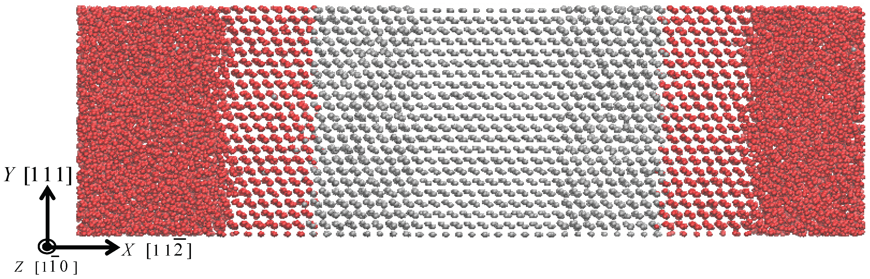
The setup of the molecular dynamics simulation cell of silicon crystal growth has been described previously [
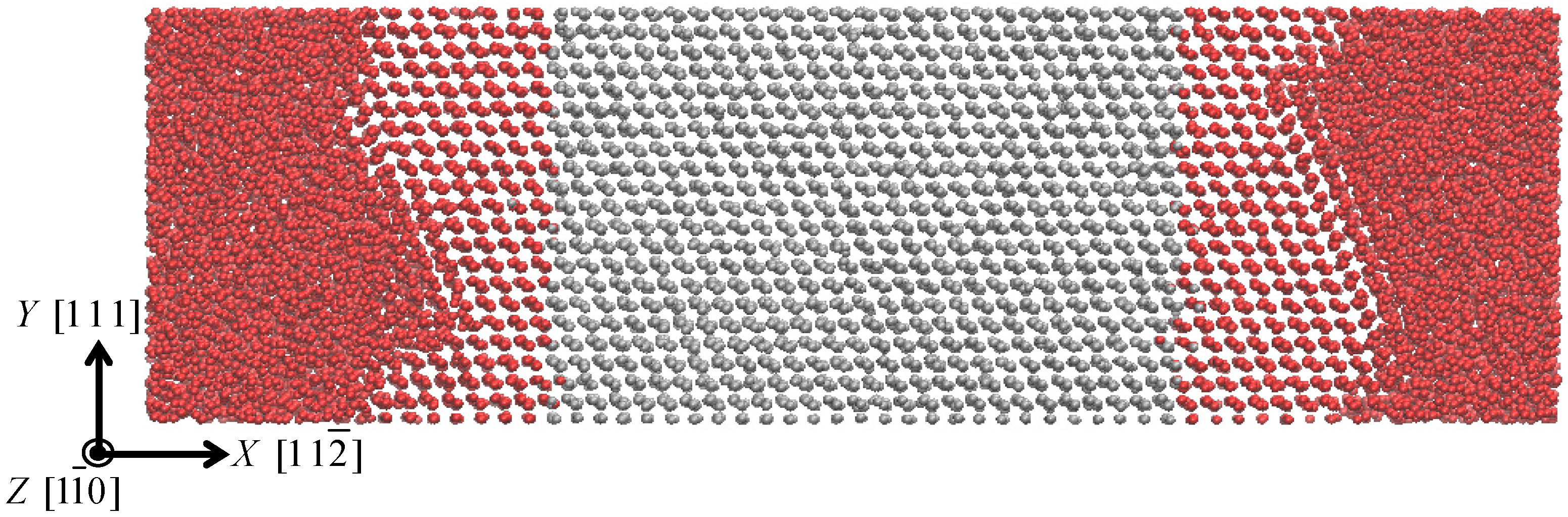
6], and for readers’ convenience it is explained briefly here. As shown in
Figure 1, the middle part of the cell with atoms in light gray represents the crystal “seeds”, and the left and right disordered parts with atoms in dark color (red) represent the silicon melt, which was obtained through a simulation of melting silicon crystal. The ordered part between the seed and the melt is the crystal grown in the simulation. The atoms from the seed and the melt are kept recorded, with their color unchanged. Due to the high temperature of the system, it is not surprising to see that some of the atoms from the “seed” dissolve into the melt, and some of the atoms from the melt diffuse into the “seed”.
Periodic boundary conditions are applied in each dimension of the cell. The growth direction is set as the X direction of the coordinate system, as shown in
Figure 1, which is a <112> direction. The other three different simulation cells, with X being an <100>, <110> or <111> direction of the crystal seed, were also set accordingly. Their initial melt parts are all set at 12 nm long on each side along the X axis. The sizes of the crystal seeds are set at about 16 nm along the X axis, and about 12 nm along Y and Z axis, for the four different simulation cells, with the detailed size satisfying the requirement of periodic borders. The cell sizes were verified to be acceptable for the respective study, by a trial simulation with a cell twice large in each dimension, and it was found that this yielded results similar to that by the simulation with the cell of the present sizes.
The inter-atomic forces are calculated with Tersoff potential [
7], which has been shown to be appropriate for modeling silicon in transition from melt to crystal [
8] and has been successfully used in simulation studies of defect formation in silicon growth from melt [
3,
6,
9]. The melting point of the silicon modeled with Tersoff potential is found to be 2480 K. A constant temperature at an undercooling of 300 K, i.e., at 2180 K, is kept by the Nose-Hoover algorithm [
10]. A space rescaling is applied to Y coordinates of the crystal seed atoms to set a uniaxial strain along the Y axis, separately for different simulations. The length of each time step is 10
−3 picosecond.
The reason for choosing an unrealistically large undercooling is to allow a sufficiently fast crystal growth so that the simulation runs can be completed in feasible lengths of time. For the same reason, unrealistically large applied strains of up to 0.08 are chosen to allow us to see the strain effect in a feasible running time. Similar compromises are often adopted in MD simulations, based on the assumption that the great acceleration would not change the qualitative feature of the concerned process. For the present study, it is expected that the qualitative dependence of the probability of dislocation formation on growth direction would not be altered by accelerating the crystal growth from melt, although a quantitative prediction cannot be expected.
3. Results and Discussion
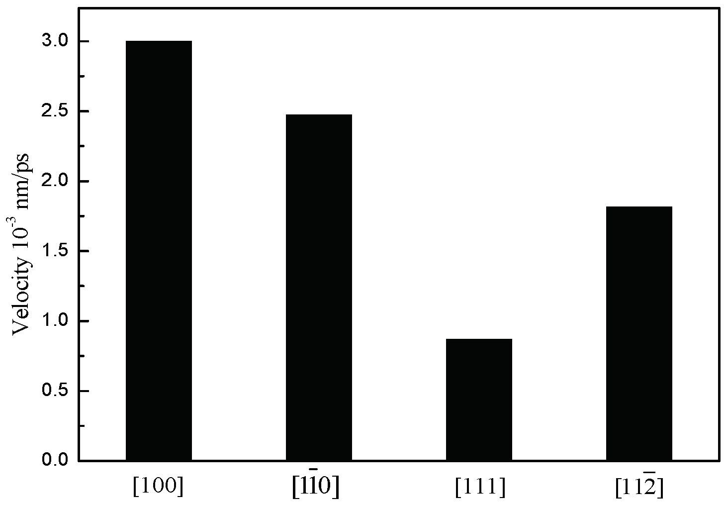
Growths of crystals along the set growth directions were observed in the simulated growths, and the growth rates were measured by counting the numbers of atoms joining the crystalline parts of the systems. The average measured growth rates are plotted in
Figure 2. As can be seen, the well-known anisotropic feature in the growth of crystalline silicon from melt [
11] is well reproduced. This result is encouraging as an indication of the basic validity of the present simulation method.
During the simulated growth of silicon from melt, the formation of dislocation is easily identified by the explicit disorders in the atomistic arrays in the newly-grown parts of the simulation cells, as described in the introduction.
Figure 3 shows such an example. Three independent simulation runs were conducted for the growth along each direction under each strain condition. The observed dislocations formed in the growths and their nucleation times were simply counted.
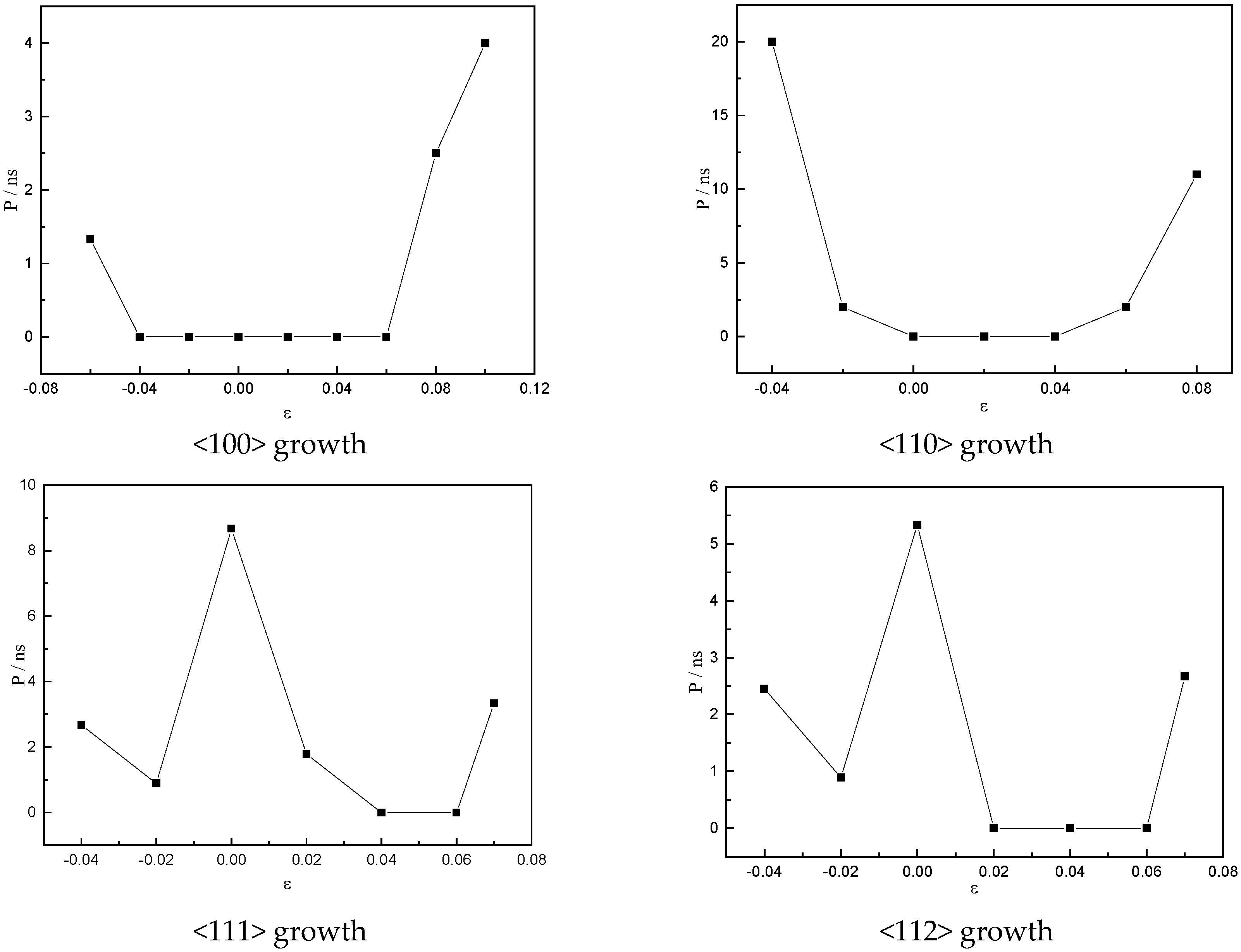
Figure 4 gives the average number of dislocations formed per nano-second as a measure of the probability of dislocation formation in the simulated growths. A great contrast in the probability of dislocation between growths along different directions is revealed. The growths under strain-free conditions confirms the previous observations [
6], and the prediction from the previous study that <111> growth will have the highest probability of dislocation formation. The previous study shows an {111}-faceting-{111}-twinning-associated mechanism of dislocation nucleation in strain-free growths [
6], which explains well the contrast by the differences in their growth surfaces’ orientations from the {111} plane, with the one with the smaller difference favoring the {111}-faceting and hence having a higher probability of dislocation formation. In contrast, a <111> growth by definition has an {111} plane as the growth surface, i.e., the crystal/melt interface, and it is readily predictable that it would yield the highest probability of dislocation formation because the {111}-faceting is no longer needed here for the {111}-twinning.
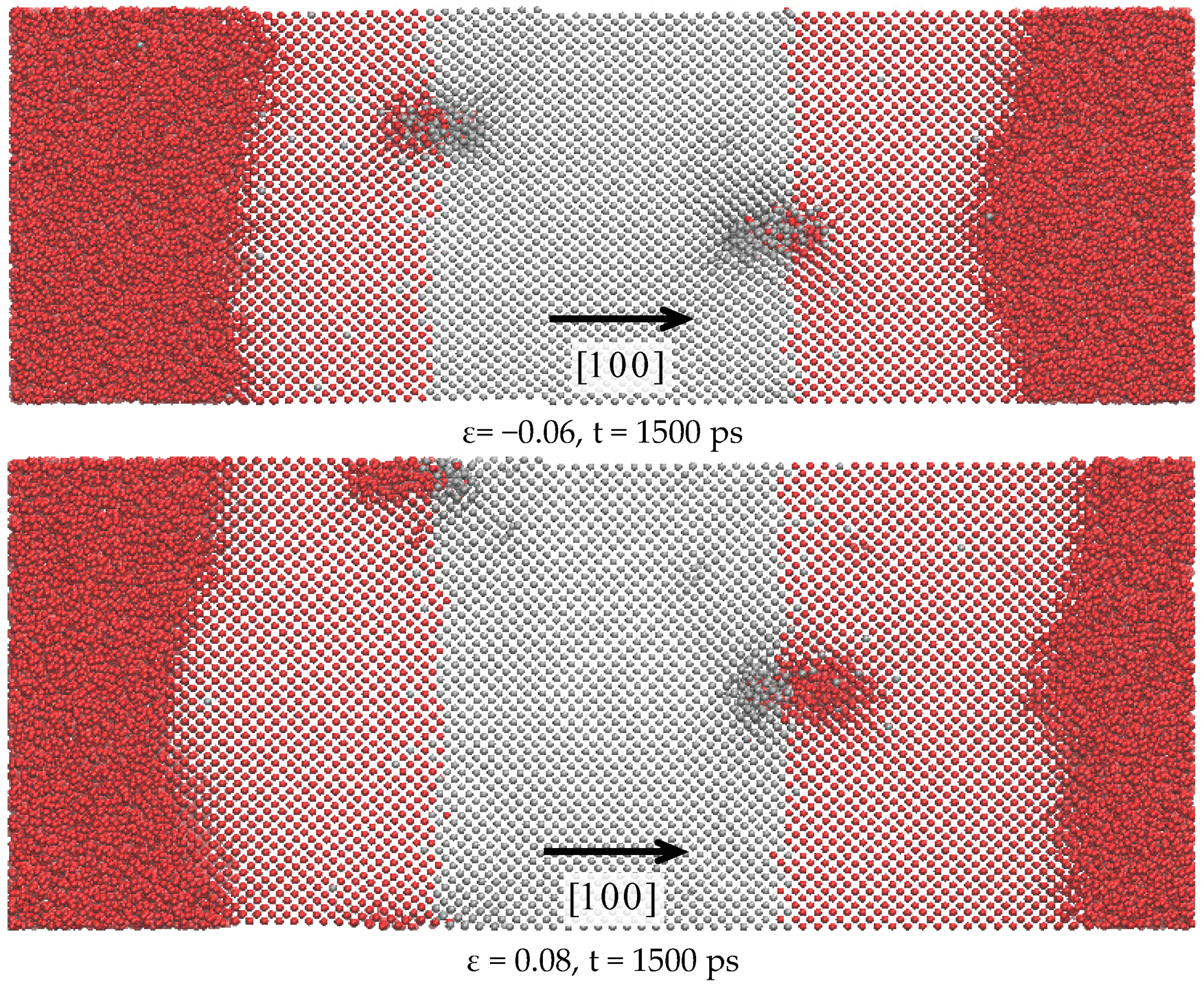
Figure 4 also shows that the growths under applied strain/stress conditions behave very differently in the formation of dislocations. In the growths along <111> and <112> directions, strains within a certain range, either tensile (ε > 0) or compressive (ε < 0), depress the dislocation formation, although strains beyond the range finally lead to an increase of the probability of dislocation formation. In the <100> and <110> growths, strains over a certain range also increase the probability of dislocation formation. It is noticed that the strain effect is not symmetrical about the 0 strain, with compressive strain being more effective than tensile strain in inducing dislocation formation.
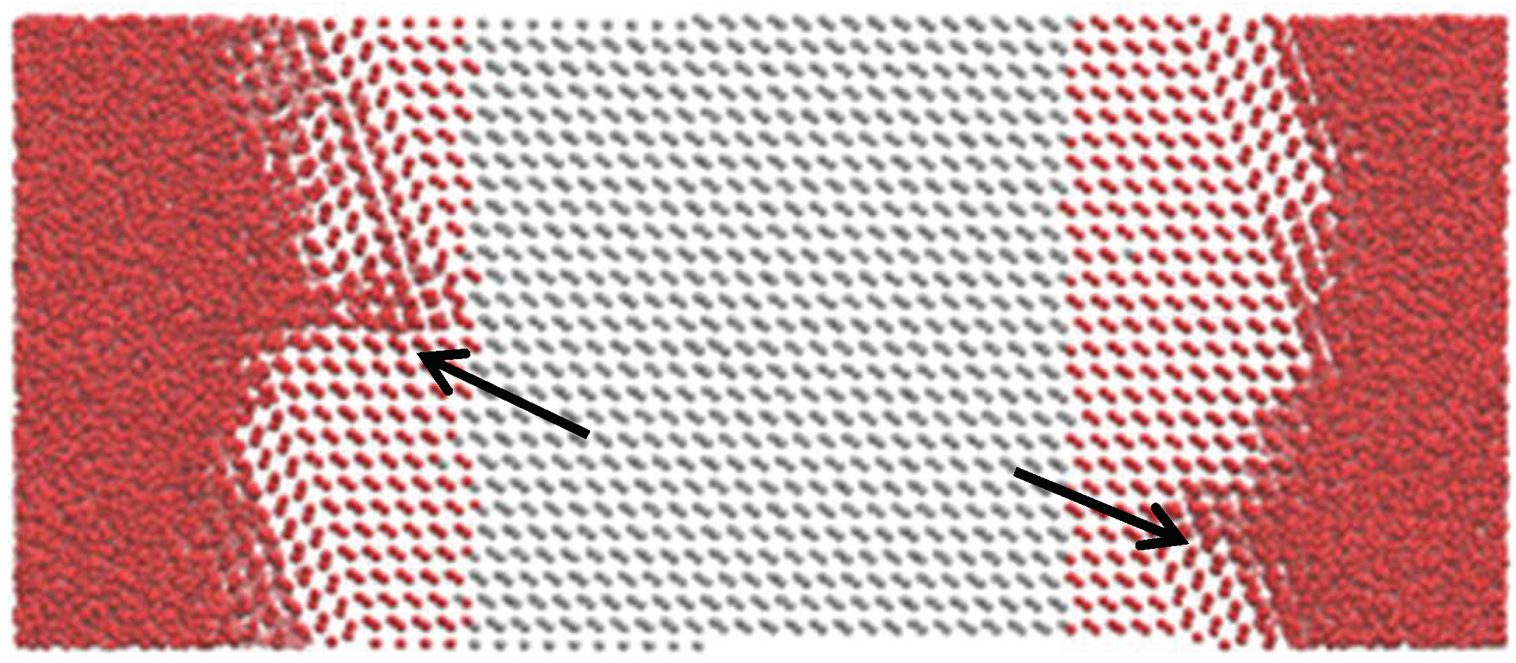
Figure 5 indicates that, in the <112> growth with a tensile strain of 0.02, {111}-faceting is no longer as developed as in the strain-free <112> growth, and the twinning does not occur. This was also observed in other cases where no dislocation was formed. We suggest that an applied uniaxial strain would inhibit the {111} twinning, meaning that the dislocation formation which relies on twinning would be inhibited.
Figure 6 shows that the structural features of the strain-induced dislocations are totally different from those formed by the faceting-twinning-associated mechanism, as shown in
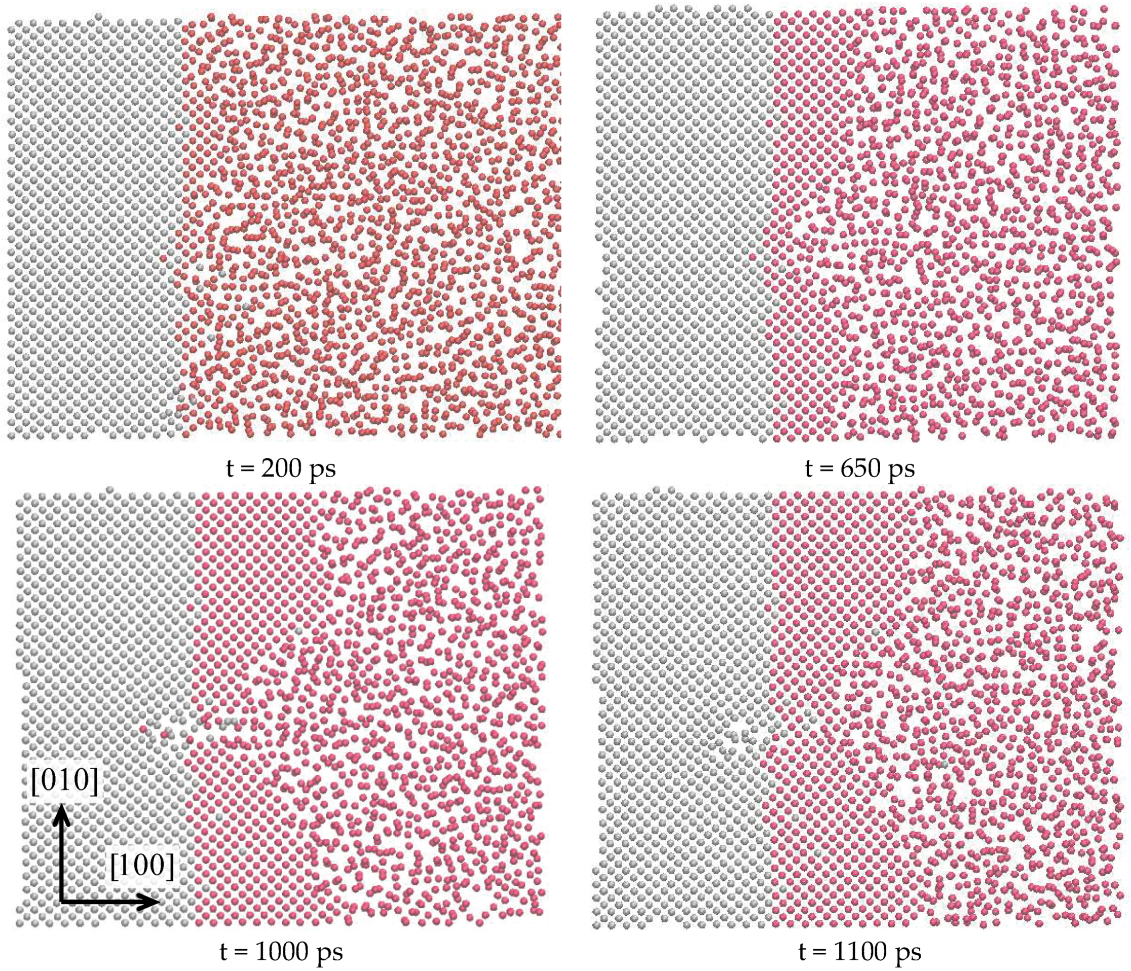
Figure 3 for example. It is believed that a different mechanism is acting here for the nucleation of dislocations in the stressed growth. Sequential observations of the dislocation process in the stressed growth are given in
Figure 7. This indicates that a randomly formed roughness feature at the growth surface was developed into a V-shaped pit, which generated disorder in the zone underneath the tip of the V-shaped pit. The local disordered zone was left behind the growth front and developed into a dislocation. Such a mechanism does not appear in stress-free growth and is believed to be strain/stress-induced.
To date, the control of growth directions in multicrystalline silicon ingots is still generally not practical in industry. In recent years, mono-like silicon ingots grown along the <100> direction by {100} seeds are attracting the renewed interest of the PV industry. The present result would strongly support such interest, as <100> growth has been found to be least probable to form dislocation as compared to growths in other directions. The results regarding the strain/stress effect should be viewed qualitatively. First, they do show that strain/stress beyond a certain range can induce dislocation formation, and secondly, they show that compressive strain/stress is more harmful than tensile.
In stress-free growths, the previously established {111}-faceting-{111}-twinning-associated mechanism of dislocation nucleation works, and hence growths with front surfaces closer to a {111} plane will favor the formation of dislocation. Strain/stress within a certain range may not induce any new mechanism of dislocation formation, while it may inhibit the above mechanism by inhibiting the {111}-twinning. The {111}-twinning is favored by the structural symmetry of {111} planes [
12], while a uniaxial strain would lower the symmetry, and hence may inhibit the twinning. Strain/stress beyond a certain range does induce new mechanism(s) of dislocation formation, while the details of the new mechanism(s) and the reason for the difference between the effects of tensile strains and compressive strains remain to be discovered.


