Review

Tunnel Junctions for III-V Multijunction Solar Cells Review

Department of Electrical and Computer Engineering, North Carolina State University, Raleigh, NC 27695, USA
*
Authors to whom correspondence should be addressed.
Crystals 2018, 8(12), 445; https://doi.org/10.3390/cryst8120445
Submission received: 24 October 2018 / Revised: 15 November 2018 / Accepted: 20 November 2018 / Published: 28 November 2018
(This article belongs to the Special Issue III-V Heteroepitaxy for Solar Energy Conversion)

Abstract

:
Tunnel Junctions, as addressed in this review, are conductive, optically transparent semiconductor layers used to join different semiconductor materials in order to increase overall device efficiency. The first monolithic multi-junction solar cell was grown in 1980 at NCSU and utilized an AlGaAs/AlGaAs tunnel junction. In the last 4 decades both the development and analysis of tunnel junction structures and their application to multi-junction solar cells has resulted in significant performance gains. In this review we will first make note of significant studies of III-V tunnel junction materials and performance, then discuss their incorporation into cells and modeling of their characteristics. A Recent study implicating thermally activated compensation of highly doped semiconductors by native defects rather than dopant diffusion in tunnel junction thermal degradation will be discussed. AlGaAs/InGaP tunnel junctions, showing both high current capability and high transparency (high bandgap), are the current standard for space applications. Of significant note is a variant of this structure containing a quantum well interface showing the best performance to date. This has been studied by several groups and will be discussed at length in order to show a path to future improvements.

1. Introduction

This review will be a discussion of both development and analysis of tunnel junction structures and their application to multi-junction solar cells. Solar energy is abundant and environmentally friendly. Efforts to generate power from solar energy have benefited from the higher efficiency of solar cell technology. The highest efficiency devices incorporate multiple solar cells in a vertically connected stack for peak efficiency at various wavelengths within the solar spectrum. These multi-junction devices require a transparent and conductive layer to join them, most commonly in the form of tunneling junctions. The first monolithic multi-junction solar cell was grown in 1980 by Bedair et al. at NCSU [1]. This solar cell used gallium arsenide (GaAs) and aluminum gallium arsenide (AlGaAs) materials which consisted of an AlGaAs-GaAs tandem cell structure utilizing a very thick (due to The liquid phase epitaxy (LPE) growth method) AlGaAs/AlGaAs tunnel junction. A further evaluation of this tunnel junction was later published [2]. The first tandem cell to achieve higher efficiency than any single cell was described in 1990 at the Solar Energy Research Institute (now NREL) [3]. This cell consisted of an InGaP-GaAs tandem cell structure utilizing a GaAs/GaAs tunnel junction. The dopants used in this second structure consisted of carbon doping for the p-type side (very common in modern structures) and selenium on the n-type side (tellurium is more commonly used today). This tunnel junction showed the advantages of newer growth methods by utilizing metal–organic chemical vapor deposition (MOCVD) to grow considerably thinner layers resulting in lower optical absorption in the tunnel junction and reduced series resistance. This type of tunnel junction was used in the first mass-produced tandem cells. Continuing advances in growth and fabrication methods have led to the use of materials and structures which improve the conductivity and transparency of modern tunnel junctions as well as industry ability to produce materials in volume at lower cost. In this review we will first make note of significant studies of III-V tunnel junction materials and performance, then discuss their incorporation into cells and modeling of their characteristics. Table 1 at the end of this review shows a timeline of the most pertinent publications.

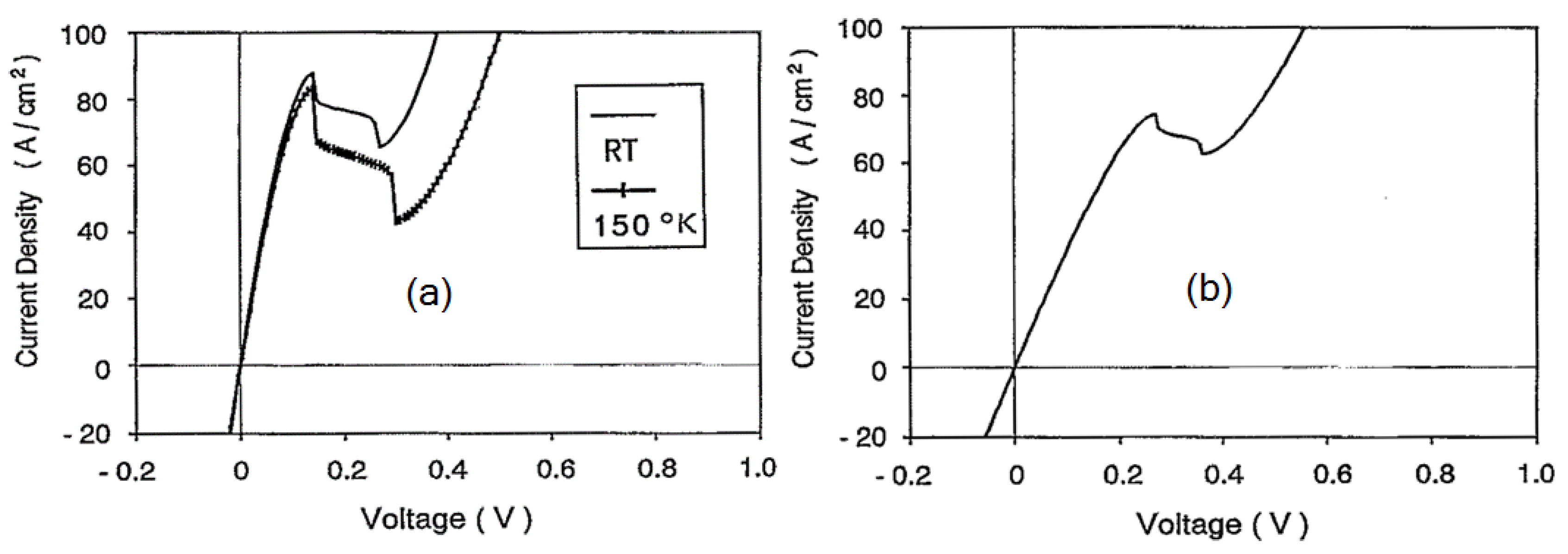
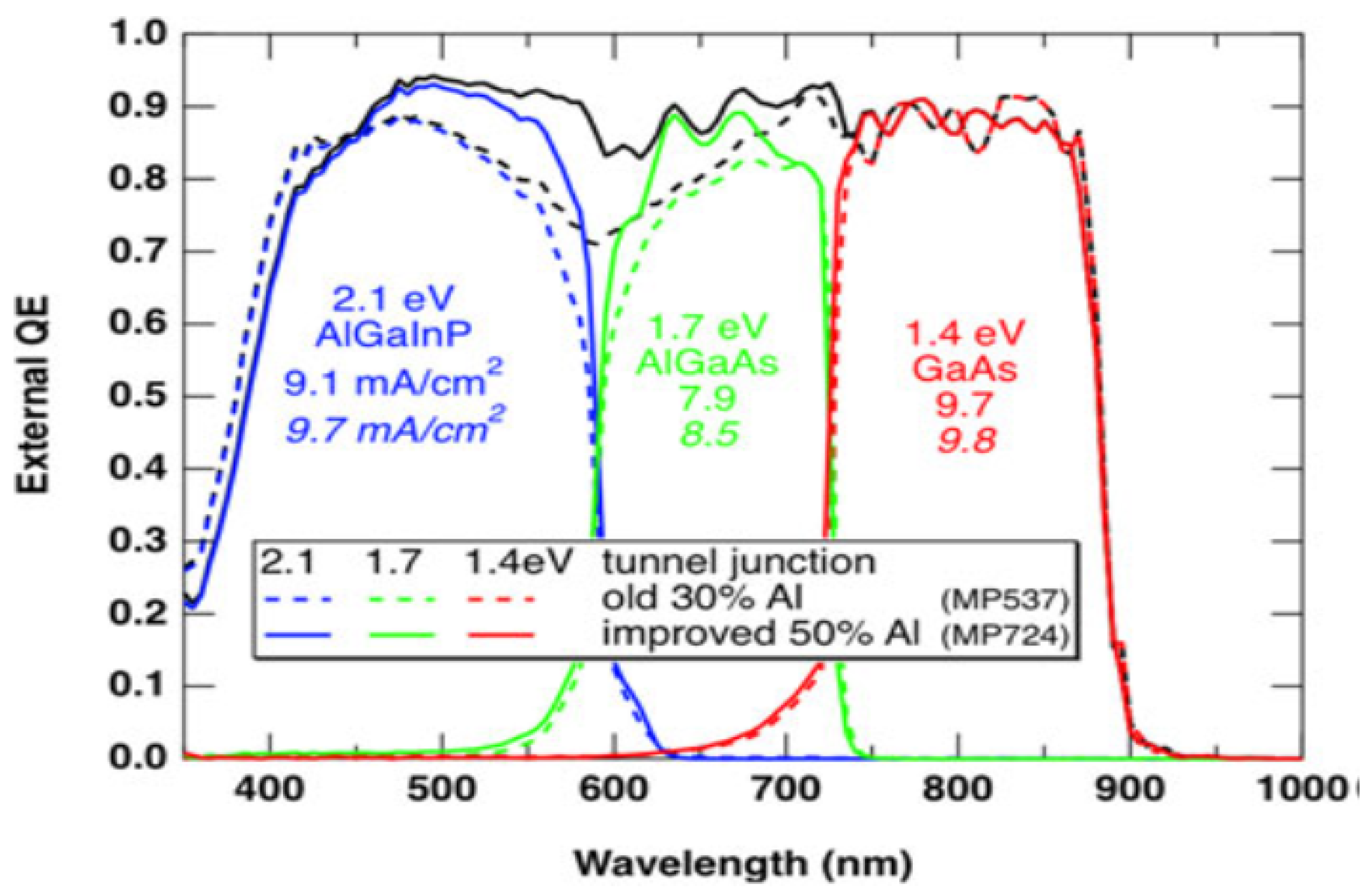
2. Studies of Various Tunnel Junctions

In parallel with and independently of the development of tandem solar cells there have been several studies of the fabrication of tunnel junctions (TJs) which we will now discuss.
These include several studies of various doping schemes for producing GaAs TJs ([4,5,6,7,8,9,10] inc. ref. therein). The tellurium-carbon doping combination in GaAs TJs has shown the best performance to such an extent that there has been little reason for further development of other dopant material within GaAs TJ systems. Despite this much work has been aimed at using this relatively simple structure to understand the mechanisms involved in practical (for solar applications) tunnel diodes. This approach has been chosen because GaAs is comparatively well characterized as compared to AlGaAs or InGaP materials [11].
Studies initially done at NTT ECL showed that a considerable reduction in diffusion of dopants in TJ structures could be achieved by using aluminum containing cladding layers [12]. It must be noted that this effect is most significant with rapidly diffusing dopants such as zinc [13]. Such highly diffusing dopants have not generally been used in later work. TJs embedded in solar cell structures have generally been clad in aluminum containing layers for other reasons such as transparent window and back surface field (BSF) layers (generally on the outside of the solar cell structure rather than the TJ). These layers provide passivation of surface or interface trap states and potential barriers for minority carriers.
The AlGaAs TJs used in the first cells grown by NCSU were quite transparent in spite of the thick layers having 35% aluminum, the same as the upper cell. When concentrator cell applications began to be considered the relatively low maximum doping that could be achieved in n-type AlGaAs worked against the use of the structure. While GaAs/GaAs TJs could provide the peak current needed for concentrator cells the optical losses, particularly in the p-type GaAs, are excessive. Since high carbon doping could be easily achieved in p-type AlGaAs grown using metal organics a TJ using a p+-type AlGaAs layer and an n+-type GaAs layer was developed at NCSU using Atomic Layer Epitaxy (ALE) [14]. This structure takes advantage of the fact that most of the absorption occurs on the p-type material in a GaAs/GaAs TJ. The n+-type side of the TJ displays a higher effective bandgap due to the Moss Burstein effect and therefore has considerably less absorption.
A relatively early attempt by TTI to produce a highly transparent structure used indium gallium phosphide (InGaP) to fabricate an InGaP/InGaP TJ [15]. Obtaining high performance for this structure has proven challenging due to a lack of any convenient way to produce highly doped p-type material in InGaP MOCVD growth with a low diffusion dopant. Carbon does not act as an acceptor in InGaP and zinc has a relatively low saturation concentration and a high diffusion coefficient at growth temperatures.
The first structure to provide a high tunneling current combined with highly transparent layers on both sides of the TJ is the n-type InGaP/p-type AlGaAs TJ. This structure was originally fabricated at NCSU by ALE using selenium as the n-type dopant in the top GaAs and InGaP layers which were grown over carbon doped p-type AlGaAs [16]. The performance of this junction is shown in Figure 1. The peak tunneling current is equal to that obtained in the lower bandgap gallium arsenide system. This is due to the high doping concentration that can be obtained in n-type InGaP and the bandgap offset between InGaP and AlGaAs which reduces the tunneling distance. Additional studies discussed later in this paper use MOCVD growth and investigated optical absorption, higher tunneling current, and incorporation into cells. Recent studies include modeling and development of very high-performance structures [17,18,19].
Unfortunately, there are relatively few studies that compare different types of TJs side by side. An exception is a study from the UO which compared AlGaAs/AlGaAs TJs with AlGaAs/GaAs and AlGaAs/InGaP TJs grown under similar conditions. In addition to experimental comparisons this study includes numerical modeling using parameters based on experimental results. While this study concluded that the AlGaAs/AlGaAs diodes were satisfactory high bandgap TJs it was noted that the AlGaAs/GaAs TJs required much lower effective doping [20]. The AlGaAs junctions fabricated in this study had sufficiently low aluminum content (20%) that they were not fully transparent. Additionally, the study was unable to duplicate the performance other groups achieved with AlGaAs/InGaP TJs. These results are consistent with results from other groups showing AlGaAs/GaAs TJs being easier to fabricate reliably when compared to AlGaAs/InGaP TJs which show a much higher sensitivity to growth conditions [21]. These details will be discussed later in this paper.
A 2013 report by 3IT-US achieved a p-type carbon doped AlGaAs/GaAs TJ with both a high aluminum composition >40% and a doping concentration reaching up to the 1020 cm−3 range using CBE [22]. This report clarified that the tunneling current is not significantly affected by aluminum concentration due to high doping levels decreasing the tunneling barrier width.
Several of the proposed high-efficiency tandem cell structures, both upright and inverted, use metamorphic layers to grow material with a larger lattice constant on gallium arsenide or germanium substrates. High concentrations of carbon doping in alloys containing high indium concentrations have proven difficult to achieve. Larger lattice constant TJs lattice matched to InGaAs layers composed of higher indium concentrations can use p-type layers consisting of gallium antimony arsenide to produce highly carbon doped material [23,24].
Another specialized TJ development is the use of erbium arsenide inclusions to produce layers which are capable of withstanding higher annealing temperatures. This has been used in MBE grown cells where low bandgap nitride containing layers require TJs which can withstand higher temperature annealing conditions [25].

3. Discussion of the Integration of Tunnel Junctions in Cells

The first tandem cells using AlGaAs TJs needed high aluminum content (35%) layers for transparency due to the LPE process producing relatively thick layers. The next notable development in tandem cells was the InGaP/GaAs tandem using GaAs tunnel junctions. This structure was feasible with the MOCVD process which allowed the growth of much thinner layers. This design was adequate for the first mass production of tandem cells. By the time a second-generation of tandem space cells was developed TJs composed of materials with lower absorption were available.
An early manufacturing [21] study at Spectrolab showed that AlGaAs/InGaP TJs produced the highest efficiency cells while also showing the cells had greater variability due to growth conditions. This report compared the performance of otherwise similar cells which used AlGaAs/InGaP TJs or GaAs/GaAs TJs. The comparison indicates about 1% absolute efficiency improvement with the higher bandgap AlGaAs/InGaP TJ. Another report [26] by the same group compared the measured and calculated absorptions of these two TJ structures. The measured and calculated absorption agreed to a value of 1.4 mA/cm2 and accounted for the 3% increase (relative to GaAs TJ) or about 1% (absolute) increase in efficiency between cells containing one of the two TJ structures. The high bandgap AlGaAs/InGaP TJ showed negligible absorption in the spectral region of importance. They also reported separately [27] an MOCVD grown AlGaAs/InGaP tunnel junction with high peak tunneling current. While these studies mention that most of the optical absorption in a GaAs/GaAs tunnel junction occurs in the p-type layer due to the Moss Burstein effect. This value actually translates to 55–60% of light absorbed in the p-type layer.This is consistent with a later report by IES-UPM of a gain of 0.56 mA/cm2 when replacing an AlGaAs/GaAs TJ with an AlGaAs/InGaP TJ [28]. Inside The IES-UPM report [28] Figure 4 shows the improvement in spectral response with the AlGaAs/InGaP TJ in the higher energy part of the GaAs cell response. This is as might be expected from the transparency of the near bandgap region seen in the report from NUB [29] on a detector based on the Burstein-Moss shift. Another report from The RIERC, which concluded that the absorption in GaAs/GaAs TJs was typically less than 1%, was concerned mostly with absorption below the GaAs bandgap energy [30].
The AlGaAs/GaAs tunnel junction is a widely used structure in concentrator cells. This structure has been used in a number of record breaking concentrator cells [31,32,33]. This is mostly due to two significant advantages: AlGaAs can be more easily doped with carbon than GaAs (which at least partially compensates for the higher bandgap) and it also seems possible that the diffusion suppressing effect of a high aluminum content layer is operative in this structure. Since the high aluminum content layer has negligible absorption in the relevant spectral region this structure eliminates somewhat over one half of the absorption of a GaAs/GaAs tunnel junction. The principal means of optimization of the AlGaAs/GaAs tunnel junction has been the minimization of the thickness of the GaAs layer. Experiments to achieve this have been described in both stand-alone tunnel junction papers [5] and in reports on the fabrication of some record holding multi-junction cells [33]. Tellurium is the most commonly used dopant since it will usually produce the highest n-type carrier concentrations, however, Te has the characteristic that during the doping growth there is some surface segregation. It therefore takes some thickness for the doping concentration to reach its full value which tends to limit the minimum thickness that can be achieved using highly Te doped GaAs layers. This effect is stronger in InGaP as will be discussed later.
Sharp Corporation likewise recognized the advantages of the AlGaAs/InGaP design for high-efficiency cells and considered it part of the later generation [34] of cell design. A modified version of this tunnel junction with a higher indium content to match 17% InGaAs was used in the record Fraunhofer ISE 41.1% cell [35]. It is worth noting that this same epitaxial structure with a different grid pattern was able to operate with high efficiency at 1700× solar concentration. Since inverted metamorphic cells have become important for record efficiency cells [31] even while using AlGaAs/GaAs TJs, it is significant that an inverted version of the AlGaAs/InGaP junction was used in the relatively recent inverted metamorphic cell of >44% efficiency developed by Sharp [36]. This demonstrated that the fabrication of high performance inverted or n on p versions of this structure are feasible.
There are two recent studies available explicitly comparing an AlGaAs/InGaP TJ to the commonly used AlGaAs/GaAs TJ in cells [28,37]. Recently NREL has developed some new tunnel junctions using p-type 60% AlGaAs and both 60% AlGaAs and InGaP n-type layers with a 12-nm GaAs quantum well in between. Both of these designs give much better performance than their previous design using 30% aluminum AlGaAs. However, in their final structure they used a quantum well thickness of 60 Å which is similar to other high transparency designs [17,28]. Figure 2 from the NREL study [37] shows how the higher transparency tunnel junction affects the spectral response of the multijunction cell. The improved high aluminum content tunnel junction produced a current improvement of about 0.6 mA in the 1.7 eV AlGaAs cell (the improvement in the AlGaInP cell is due to lower Se in the window) as is shown in Figure 2, which is approximately the same increase as was seen by IES-UPM [28]. Similarly to the report of IES-UPM, the improvement is seen only in the higher energy part of this cells spectral response. It is also about the same improvement that would be expected based on the results of the earlier Spectrolab study [21] which had demonstrated that the AlGaAs/InGaP TJ would produce higher efficiency cells than other available designs but initially was not as reliable a process.

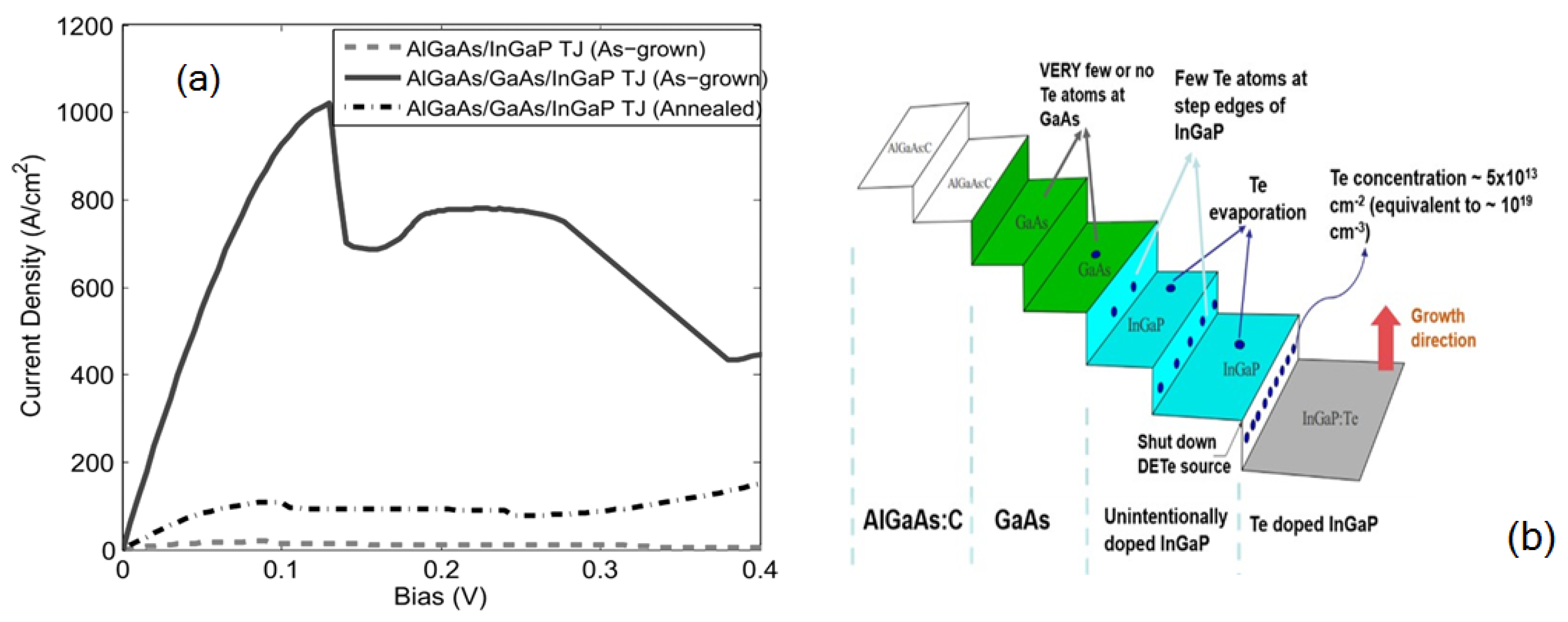
4. Detailed Discussion of AlGaAs/InGaP Tunnel Junction Fabrication
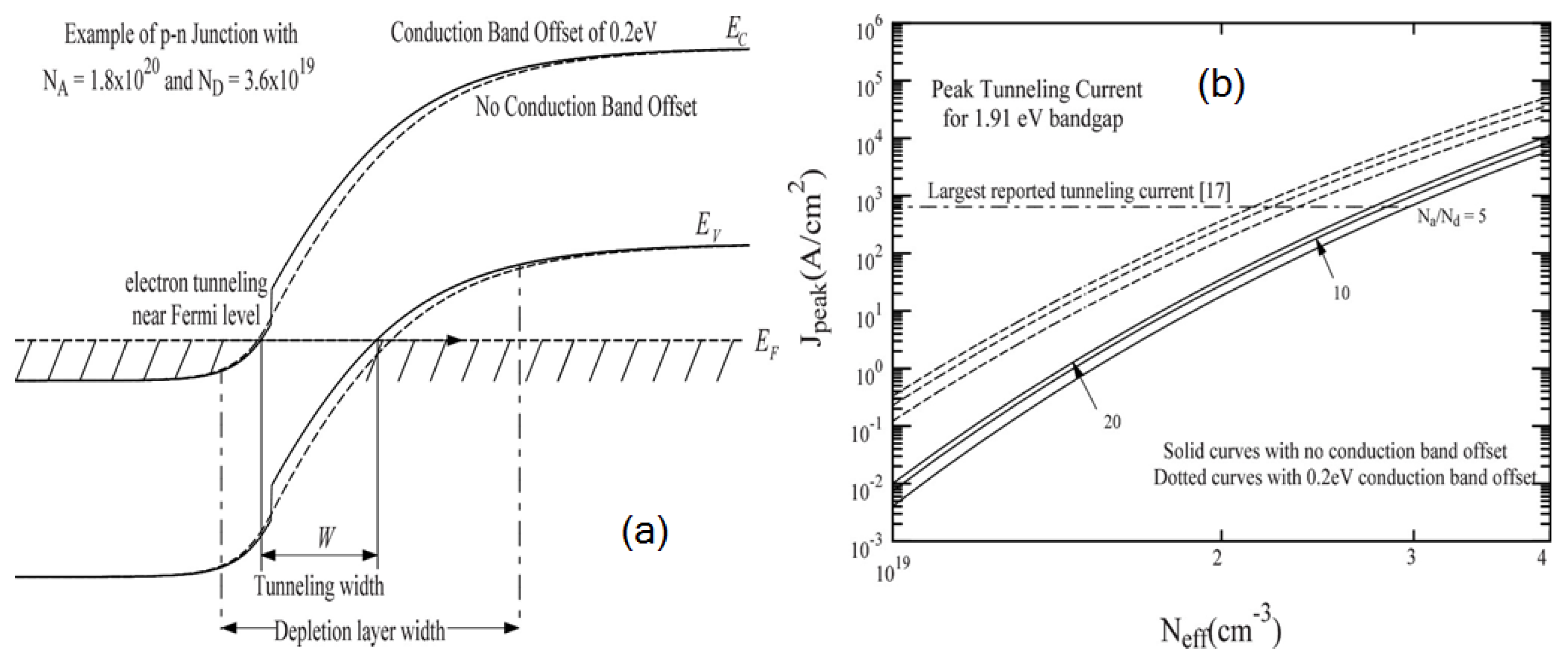
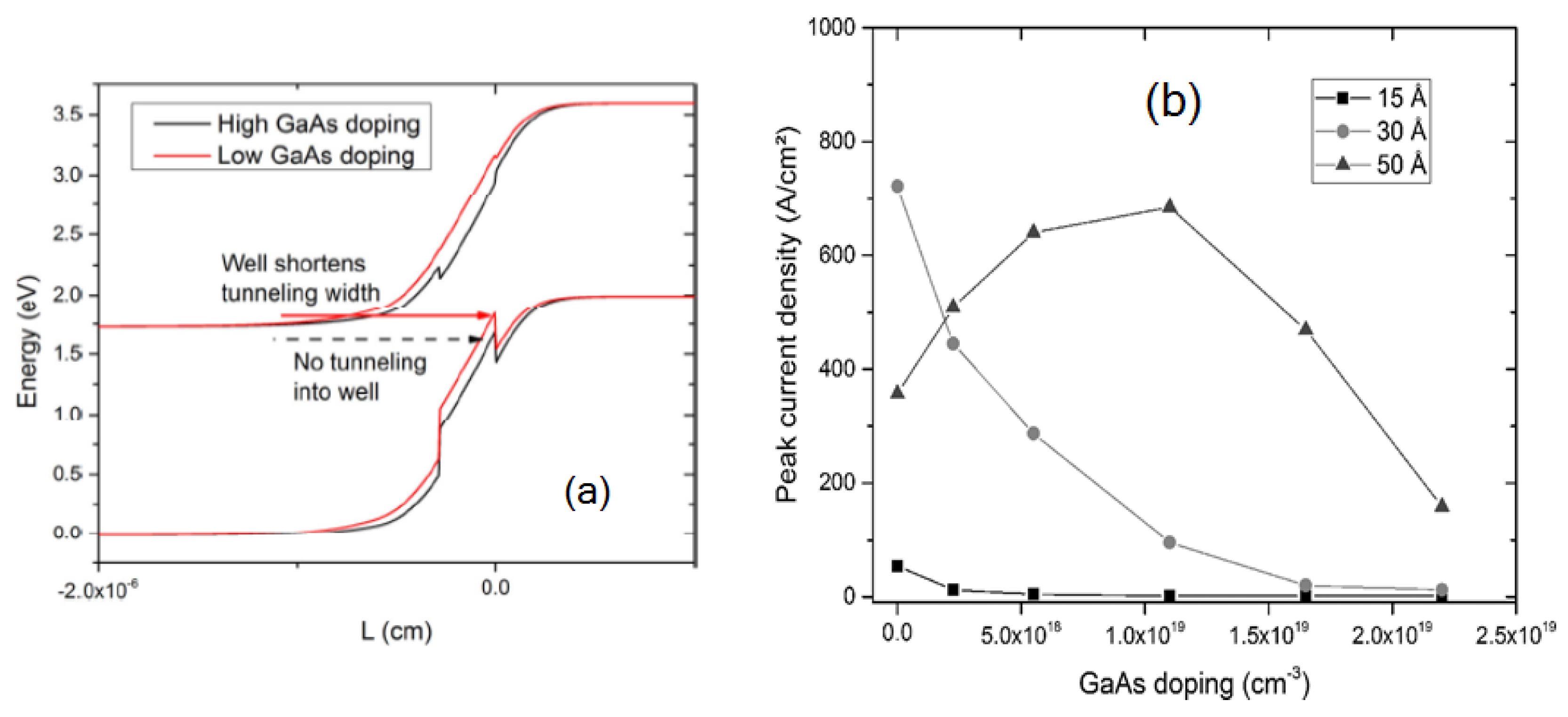
Because the AlGaAs/InGaP tunnel junction provides the highest-performance of the high transparency tunnel junctions it will be discussed in more detail. As was previously mentioned achieving reproducible fabrication has been more difficult than for other tunnel junctions. This is due to several factors, probably the most important factor being tellurium segregation on the growing surface under high doping conditions [38,39]. This makes fabrication of this basic structure very sensitive to the exact growth procedures followed at the interface of the junction. One report by VII [38] found that pausing growth and raising the temperature of the InGaP surface before starting growth of the AlGaAs layer, thus preventing carryover of tellurium into the AlGaAs layer, was necessary to fabricate good tunnel junctions.
More recently, higher performance [17] has been achieved by the Bedair group at NCSU in AlGaAs/InGaP tunnel junctions by including a very thin GaAs layer in between the InGaP and the AlGaAs layers. This is consistent with tellurium accumulation on growing GaAs surfaces being less than on InGaP surfaces in agreement with an earlier report from IES-UPM [39]. This interlayer is of quantum well thickness at around 50 Å or less and has a twofold effect on the tunnel junction characteristics: it serves to reduce the carry-over of tellurium into the AlGaAs layer and the quantum well energy level produces increased tunneling current. The effect is large as can be seen in Figure 3a, which shows the characteristics of otherwise similar TJs with and without the GaAs interlayer. Figure 3b illustrates the effect of tellurium segregation on the growth surface.
The stability under annealing conditions was drastically improved by using a slower growth rate and by cutting off the flow of tellurium early to allow the tellurium accumulation on the surface to dissipate. Both of these procedures would be expected to reduce the defect concentration in the as grown film and presumably even more so in the annealed structure. Figure 4 shows the much greater stability of a structure grown under these conditions as compared to the structure shown in Figure 3a.
A report by IES-UPM on the doping of InGaP with diethyl-tellurium [39] confirms that there is a surface accumulation phenomena large enough to seriously affect the indium/gallium incorporation ratio. This makes the effects obtained by the early cut off of tellurium in tunnel junction growth seem reasonable. The importance of tellurium surface segregation is emphasized by the sensitivity of the tunnel junction characteristics to the details of the tellurium cutoff procedure during the growth. The effect has been reported by a number of different laboratories [19,28,38,39,40].
There is also a report from TSAR on the doping of InGaP with diisopropyl-telluride (DIPTe) and the growth of TJs with this dopant [40]. It is worth noting that in this work, there is no large effect on the indium to gallium ratio as seen from the diethyl-telluride (DETe). The accumulation of tellurium on the surface of the InGaP was removed from the metallurgical tunnel junction by holding at a growth temperature of 580 °C for 15 min. under an arsenic atmosphere. It seems reasonable that this step will remove the adsorbed tellurium on the surface. Additionally this will also probably produce a monolayer or two of InGaAs at the surface which may act as a quantum well at the junction as has been used in other structures [17,19,28]. It is also noteworthy that in this investigation the same procedure had to be used at the interface between the low doped buffer layer and the highly doped TJ layer. It seems possible that this procedure also removed grown in defects, perhaps in a similar way to the lower defect concentration produced by reduced growth rates in other laboratories [19]. Unfortunately there is no high temperature annealing data reported in this work. An interesting aspect of this work is the growth of TJs both n-up and p-up, high (though not record) performance was obtained in both cases. This is important since much of the high-efficiency work is proceeding on inverted structures which require the junctions to be grown n-up rather than the p-up junctions which are more widely studied for upright cell use.

5. Modeling

While empirical methods have been developed for producing satisfactory tunnel junctions for concentrator cell applications, a deeper understanding of the TJs is still elusive.
The GaAs/GaAs TJ has probably had the most analysis. This is important because GaAs is a much better characterized material than ternary III-V [11,41] compounds used in high performance TJs and thus the GaAs structures can provide validation of proposed models for the less well understood materials. The development of TJ modeling has been somewhat complicated. Several studies have concluded that the properties of the GaAs/GaAs TJ are adequately explained in the region of peak tunneling current by direct band to band tunneling generally following the analytical methods of Kane at HRL [42,43] and numerical calculations developed from them [19,44] at NCSU using existing methods [45,46]. however, one study from PUM [8] has been cited repeatedly [28,47] by IES-UPM to support a conclusion that trap assisted tunneling dominated by nonlocal resonant tunneling through defects is necessary to explain the data in high performance devices. The reason in the PUM study for this contention is that their calculation of the band to band tunneling is much lower than that computed by other groups and thus will not account for the observed tunneling current. A probable reason for this discrepancy has been found in an analysis from UT [48] that considers the band to band coupling (mixing) of the conduction band and the light hole valence band which will reasonably account for the observed tunneling current at doping densities below the level at which band narrowing effects may dominate. A subsequent analysis [49] refined this calculation and found agreement with a more complete non-equilibrium Green’s function formalism (NEGF) [50,51] calculation. However, quantitative agreement with experimental results was achieved only by using bandgap narrowing as a fitting parameter as there is no complete theory for this effect. One point worth noting is that earlier experiments on germanium tunnel diodes showed that when a large number of defects were added by irradiation (neutrons) the valley current increased but the tunneling current peak was not effected very much [52,53,54]. Also gold doped silicon tunnel diodes exhibited mainly increased valley current with increasing gold concentration [55]. This argues against the peak tunneling current being due to traps. Numerical analysis utilizing commercial software (Synopsis Device) [20,56] have typically concluded that band-to-band tunneling explains the peak currents although these numerical models contain a fair number of fitting parameters. Some of the experimental data contain fairly high valley currents which almost all models regard as coming from trap assisted tunneling effects. However, a recent study of GaAs/GaAs tunnel diodes [6] which used band gap narrowing data from photoluminescence as well as the methodology used for the initial AlGaAs/InGaP analyses [9,44] concluded that band to band tunneling will account for the current when the effective tunneling barrier thickness of the depletion layer is properly accounted for. It is also worth noting that the temperature dependence of the peak current as discussed in [28] is not straightforward in other systems. It is controlled by a balance between the temperature dependence of the bandgap and that of the density of states [53] and can thus vary with the doping densities.
The only detailed modeling of the AlGaAs/GaAs structure uses numerical analysis from the Synopsis Device commercial software package [57] and concluded that this structure needed a much lower effective doping than other structures for the same peak current. It even suggested that this structure might have a peak current of 10,000 A/cm2 at attainable doping levels.
The first thorough analytic analysis of the empirically developed AlGaAs/InGaP structure was published by the Bedair group at NCSU in 2010 [44]. The approach used the methodology of Kane [58] which was extended by numeric integration taking into account published bandgap narrowing models and band offsets. A diagram of the bandgap lineup and tunneling distances is shown in Figure 5a and the expected peak tunneling currents calculated in this way are shown in Figure 5b. An approach which was broadly similar was later used by HRL [43] to get good agreement with the experimental data in silicon tunnel diodes [59]. This study showed that very high tunneling currents were predicted when the bandgap narrowing effects of the high doping levels attainable in n-type InGaP and the favorable bandgap offset of InGaP with AlGaAs were taken into account. From Figure 5b, it is clear that a reasonable band offset is responsible for about an order of magnitude higher tunneling current in this heterojunction.
After it was discovered that the inclusion of a quantum well layer led to greatly improved performance [17], a modeling effort was initiated to understand this phenomena. Figure 6a shows the band diagram for a heterojunction with a GaAs quantum well at the interface. After the improved annealing performance with low growth rate and early Te cut-off was discovered [18] a more sophisticated modeling effort was undertaken. Since the constant field approximation from the HRL paper would not be applicable to the structure with the quantum well, the tunneling current was calculated using the Esaki expression for tunneling in a given field and numerically integrating Poisson’s equation across the junction using a transfer matrix approach taking the expected band narrowing and band offsets into account [19]. The results shown in Figure 6b indicate that there is an optimal doping level for the quantum well that is lower than the maximum that can be attained in junctions of this type. This result is helpful in explaining the favorable result of the early tellurium cutoff as well as the effectiveness of a nominally carbon doped 30 Å layer in other experiments [28]. It is worth noting that improved performance has been achieved in InP based systems with a double quantum well structure [60] and successfully modeled with nonequilibrium Green’s function formalism (NEGF) [61]. This modeling approach has also been applied to other tunnel junctions [51,62].

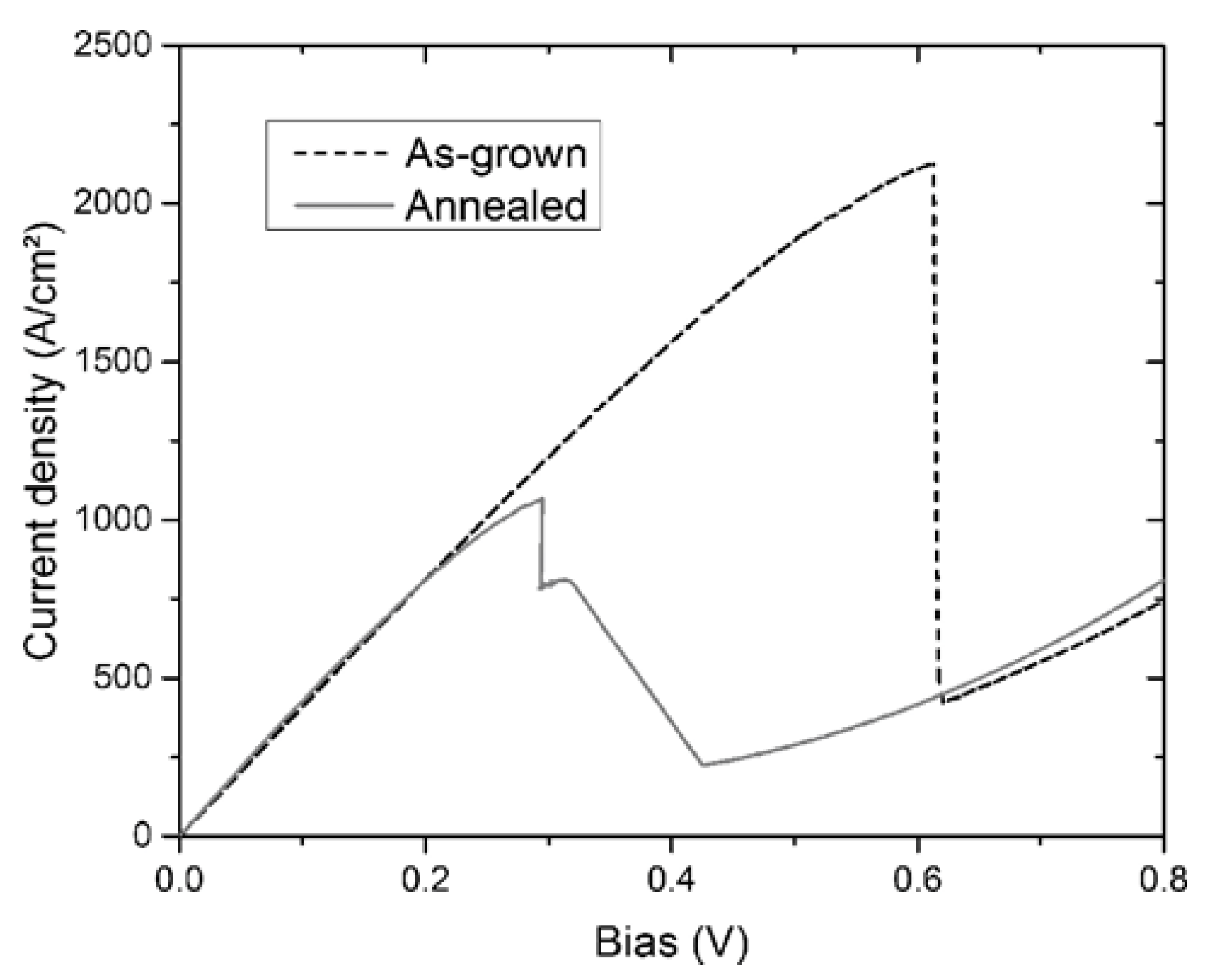
6. Thermal Stability

There are two major problems in the fabrication of TJs for use in multi-junction solar cells: The initial growth of the TJ with the necessary characteristics and its stability while the rest of the cell structure is being grown. This latter condition is significant since high-performance cell structures are typically grown at higher temperatures than optimal TJs. In many of the experimental TJ structures large annealing effects have been seen. In general there are several competing explanations for these effects. Modeling of this process and the consequent change in tunnel junction characteristics is in a much less developed state than the modeling of the as grown characteristics.
The obvious assumption is that the deterioration is due to inter-diffusion at the junction. While this might have been important with some early junctions using fast diffusing dopants (i.e., Zn) [13,15,63] the reports of studies searching for this effect in later junctions grown with slow diffusers (Te, Se ,C) have been negative [28]. (Admittedly there are no studies with the resolution comparable to that seen in studies of carryover phenomenon in superlattice growth [64]).
There are several other possibilities. If the tunneling current proceeds through traps then it is reasonable to think that the traps might be annealed out by high temperature annealing. However, it is established [53,55] that trap related processes primarily contribute to the valley current and thus a trap reduction would be expected to reduce current more than proportionately which does not generally appear to be the case. It also seems likely that the TJ structures grown at low growth rates or annealed at higher growth temperature have fewer defects than the high growth rate structures. The higher growth rate structures show more current loss than the lower defect structures after annealing.
The mechanism that is the most likely to dominate the annealing effects is one recently discussed by IES-UPM [65]. Their proposal is that annealing causes a reduction in net carrier concentration via compensating dopants (more favorable to donors) by changing native amphoteric defect sites (either thermally generated or already present, vacancies in this report). The driving potential for defect compensation is stated as the difference between the Fermi level and a Fermi Level Stabilization Energy which is determined by the energy level of stoichiometric defects. This behavior would be in accord with the explanation from LBNL of the maximum donor concentrations that are stable in III-V materials given that it has been found possible to incorporate more tellurium (and other donor dopants) than are electrically active [66]. This limit is based on compensation by complexing with stoichiometric defects. They have verified experimentally that under annealing conditions a reduction in carrier concentration is seen in highly doped low growth temperature GaAs layers which, using an analysis similar to that of Hauser at NCSU [44], is sufficient to account for the reduction of tunneling current seen in tunnel junctions using similar n-type GaAs layers. Additional support for this explanation is provided by the reported behavior of highly doped n-type InGaAs [67]. In the InGaAs case layers with several times 1019 n-type carriers can be grown at low temperatures. However, when these are annealed at higher temperatures the concentration converges to about 1.5 × 10¹⁹ which is the same carrier concentration that can be achieved by ion implantation in the layers. This behavior is believed to be related to defect chemistry [66]. However, we have not been able to find any direct reports in the literature discussing the annealing of highly doped InGaP layers.
Another factor to be remembered is that knowledge of the details of the band tails producing band gap narrowing is only approximate. There is no detailed study that we are aware of that investigates the effect of annealing on the details of the edge of the bandgap narrowing in these materials. The reduction of the peak voltage range seen in Figure 4 would suggest a reduction of band gap narrowing after annealing if the analysis of peak broadening is similar to that in silicon [59].

7. Conclusions

The first proof of concept monolithic tandem cell used an AlGaAs/AlGaAs tunnel junction due to factors involved in liquid phase epitaxy, significantly the high thickness required more transparency. The first widely produced cells used GaAs/GaAs tunnel junctions with much thinner layers grown by MOCVD. This empirically developed junction was satisfactory for first-generation cells. Subsequent work on GaAs/GaAs TJs was aimed largely at understanding the junctions since a GaAs homo-junction could be more easily modeled. Most [6,9,10], though not all [8], of the reports on modeling concluded that direct tunneling (particularly if bandgap narrowing effects were added) adequately explained the tunneling currents observed. This discrepancy was resolved when it was shown [48] that the current in lower doped structures could be explained by direct tunneling if band coupling (mixing) effects were included. Once the carbon doping procedure for GaAs was developed the p+ AlGaAs/n+ GaAs tunnel junction was easy to implement and eliminated somewhat more than half of the absorption of GaAs/GaAs junctions. This structure was widely used in a number of record setting concentrator cells but was not as extensively studied or modeled. However, there was one modeling study (using a commercial software package) comparing this structure with other structures. This study showed that the AlGaAs/GaAs structure provided the highest conductance with equivalent doping compared to other structures and predicted that a peak tunneling current of 10,000 A/cm2 was possible with plausible doping levels. Later experimental work achieved this current [47]. Recent work has shown that highly doped p-type AlGaAs containing a high aluminum content will produce junctions of equal electrical performance to those fabricated with lower aluminum content while providing higher transparency [22]. The first all high bandgap TJ with a high peak tunneling current was The AlGaAs/InGaP junction which was fabricated by ALE [16]. When the MOCVD grown version was incorporated into tandem cells it provided about 1% absolute efficiency increase over the GaAs/GaAs junctions previously used [21]. It became the standard Junction for high-efficiency one sun cells and was also used in some record-breaking concentrator cells [35]. however, the AlGaAs/InGaP TJ was found to be relatively difficult to fabricate with high yields and high-performance. The high-performance of this junction is attributed to the relative ease of doping InGaP highly n-type as compared to GaAs and to the favorable band offset between InGaP and AlGaAs. While this junction began to be used circa year 2000, detailed modeling demonstrating this explanation was not reported until 2010 [44]. The modeling followed the approach of Kane at HRL [42] and additionally took both bandgap narrowing and the bandgap offset between materials into account. The resulting approach is thus analogous to later work which provided a good analysis of silicon tunnel junctions [59]. Later experimental work with the structure showed that the addition of a thin GaAs quantum well at the junction provided a record peak tunneling current for a junction of this bandgap. Other work suggested that tellurium segregation on the surface of the growing InGaP might be the cause of the difficulties that are found in growing the structure reliably. A later experiment with an early tellurium cut off showed record performance for an annealed tunnel junction.
Structures of similar design with a quantum well in-between the InGaP and the AlGaAs have been fabricated in several laboratories and found to have high performance. When incorporated into multi-junction cells these QW containing devices have provided the predicted 0.6 mA one sun current increase. It thus appears that this design or a variant using AlGaAs instead of InGaP will become the standard for new high-performance concentrator cell designs.
Detailed modeling of GaAs tunnel junctions [49] using non-equilibrium Green’s function formalism (NEGF) [50,51] combined with the previous success of this approach on more complex structures [61] provides a promising approach for future modeling of high performance tunneling structures.
Recent work by IES-UPM [65], which had previously argued [35,37] for the dominance of trap related tunneling in the peak current, now supports the direct tunneling model and provides an important advance in the understanding of annealing effects. This study states that degradation of tunneling current has been observed in tunneling junctions regardless of the material system. This reduced current is explained by compensation of dopants via generation of amphoteric native defects becoming vigorously energetically favorable in highly doped material. This mechanism is basically the same mechanism which makes it impossible to grow highly doped uncompensated films at the higher annealing temperatures.

Author Contributions

Article was drafted by P.C. and revised and edited by B.H. and S.B.

Funding

This research was funded by The National Science Foundation research grant DMI-1102060 “GOALI: Cooperative Integration of High Efficiency Multijunction Solar Cell Structures” and by the US Department of Energy EERE SETP CSP subprogram grant DE-EE000540 “Technology Enabling Ultra High Concentration Multi-Junction Cells”.

Acknowledgments

Our work in this area of research has been supported by both the National Science Foundation and the Department of Energy.

Conflicts of Interest

The authors declare no conflict of interest influencing The representation or interpretation of reported research results in the design of the study; in the collection, analyses or interpretation of data; in the writing of the manuscript, or in the decision to publish the results must be declared in this section. The founding sponsors had no role in the design of the study; in the collection, analyses, or interpretation of data; in the writing of the manuscript, and in the decision to publish the results.

Abbreviations

The following abbreviations are used in this manuscript:
3IT-USInterdisciplinary Institute for Technological Innovation University of Sherbrooke
ALEatomic layer epitaxy
AlGaAsaluminum gallium arsenide
BSFback surface field
CBEchemical beam epitaxy
DETediethyl-telluride
DIPTediisopropyl-telluride
EQEExternal Quantum Efficiency
Fraunhofer ISEFraunhofer Institute for Solar Energy Systems
GaAsgallium arsenide
IES-UPMSolar Energy Institute of The Universidad Politécnica de Madrid
InGaAsindium gallium arsenide
InGaPindium gallium phosphide
LPEliquid phase epitaxy
LBNLLawrence Berkeley National Laboratory
MBEmolecular beam epitaxy
MJSCMulti-Junction Solar Cell
MOCVDmetalorganic chemical vapor deposition
NCSUNorth Carolina State University
NEGFNone-Equilibrium Green’s Function
NRELNational Renewable Energy Laboratory
NTT ECLNTT Electrical Communications Laboratories
NUBNortheastern University Boston
PUMPhilipps University Marburg
RIERCRockwell1 International Electronics Research Center
TJtunnel junction
TSARTotal S.A. Renewables
TTIToyota Technological Institute
UOUniversity of Ottawa
UTUniversity of Toulouse
VIIVeeco Instruments Inc.

References

  1. Bedair, S.M.; Lamorte, M.F.; Hauser, J.R. A two-junction cascade solar-cell structure. Appl. Phys. Lett. 1979, 34, 38–39. [Google Scholar] [CrossRef]
  2. Bedair, S.M. Properties of p+-n+ AlGaAs diodes. J. Appl. Phys. 1980, 51, 3935–3937. [Google Scholar] [CrossRef]
  3. Olson, J.M.; Kurtz, S.R.; Kibbler, A.E.; Faine, P. A 27.3% efficient Ga0.5In0.5P/GaAs tandem solar cell. Appl. Phys. Lett. 1990, 56, 623–625. [Google Scholar] [CrossRef]
  4. Beji, L.; El Jani, B.; Gibart, P.; Portal, J.C.; Basmaji, P. Hydrostatic pressure studies of GaAs tunnel diodes. J. Appl. Phys. 1998, 83, 5573–5575. [Google Scholar] [CrossRef]
  5. Bauhuis, G.J.; Mulder, P.; Schermer, J.J. Ultra-thin, high performance tunnel junctions for III-V multijunction cells. Prog. Photovolt. Res. Appl. 2014, 22, 656–660. [Google Scholar] [CrossRef]
  6. Lebib, A.; Hannanchi, R.; Beji, L.; EL Jani, B. Effect of band gap narrowing on GaAs tunnel diode I-V characteristics. Phys. B Condens. Matter 2016, 502, 93–96. [Google Scholar] [CrossRef]
  7. Cunningham, B.T.; Guido, L.J.; Baker, J.E.; Major, J.S.; Holonyak, N.; Stillman, G.E. Carbon diffusion in undoped, n-type, and p-type GaAs. Appl. Phys. Lett. 1989, 55, 687–689. [Google Scholar] [CrossRef]
  8. Jandieri, K.; Baranovskii, S.D.; Rubel, O.; Stolz, W.; Gebhard, F.; Guter, W.; Hermle, M.; Bett, A.W. Resonant electron tunneling through defects in GaAs tunnel diodes. J. Appl. Phys. 2008, 104, 094506. [Google Scholar] [CrossRef]
  9. Beji, L.; El Jani, B.; Gibart, P. High quality p+-n+-GaAs tunnel junction diode grown by atmospheric pressure metalorganic vapour phase epitaxy. Phys. Status Solidi A Appl. Res. 2001, 183, 273–279. [Google Scholar] [CrossRef]
  10. Zahraman, K.; Taylor, S.; Beaumont, B.; Grenet, J.; Gibart, P.; Verie, C. Efficient GaAs tunnel diode as an inter-cell ohmic contact in the tandem AlxGa1−xAs/GaAs. In Proceedings of the Conference Record of the Twenty Third IEEE Photovoltaic Specialists Conference—1993 (Cat. No.93CH3283-9), Louisville, KY, USA, 10–14 May 1993; pp. 708–711. [Google Scholar]
  11. Schubert, E.F. Doping in III-V Semiconductors; Cambridge University Press: Cambridge, UK, 1993; p. 606. [Google Scholar]
  12. Sugiura, H.; Amano, C.; Yamamoto, A.; Yamaguchi, M. Double heterostructure GaAs tunnel junction for a AlGaAs/GaAs tandem solar cell. Jpn. J. Appl. Phys. 1988, 27, 307–310. [Google Scholar] [CrossRef]
  13. Kojima, N.; Okamoto, M.; Taylor, S.J.; Yang, M.J.; Takamoto, T.; Yamaguchi, M.; Takahashi, K.; Unno, T. Analysis of impurity diffusion from tunnel diodes and optimization for operation in tandem cells. Sol. Energy Mater. Sol. Cells 1998, 50, 237–242. [Google Scholar] [CrossRef]
  14. Eldallal, G.M.; Hayafuji, N.; Elwaffa, M.S.A.; Elgammal, M.A.; Bedair, S.M. Al0.3Ga0.7As/GaAs heterojunction tunnel diode for tandem solar cell applications. AIP Conf. Proc. 1994, 306, 550–557. [Google Scholar]
  15. Takamoto, T.; Yumaguchi, M.; Ikeda, E.; Agui, T.; Kurita, H.; Al-Jassim, M. Mechanism of Zn and Si diffusion from a highly doped tunnel junction for InGaP/GaAs tandem solar cells. J. Appl. Phys. 1999, 85, 1481–1486. [Google Scholar] [CrossRef]
  16. Jung, D.; Parker, C.A.; Ramdani, J.; Bedair, S.M. AlGaAs/GaInP heterojunction tunnel diode for cascade solar cell application. J. Appl. Phys. 1993, 74, 2090–2093. [Google Scholar] [CrossRef]
  17. Samberg, J.P.; Zachary Carlin, C.; Bradshaw, G.K.; Colter, P.C.; Harmon, J.L.; Allen, J.B.; Hauser, J.R.; Bedair, S.M. Effect of GaAs interfacial layer on the performance of high bandgap tunnel junctions for multijunction solar cells. Appl. Phys. Lett. 2013, 103, 103503. [Google Scholar] [CrossRef]
  18. Bedair, S.M.; Carlin, C.Z.; Harmon, J.L.; Hashem Sayed, I.E.; Colter, P.C. High performance tunnel junction with resistance to thermal annealing. AIP Conf. Proc. 2016, 1766, 020003. [Google Scholar] [Green Version]
  19. Bedair, S.M.; Harmon, J.L.; Carlin, C.Z.; Hashem Sayed, I.E.; Colter, P.C. High performance as-grown and annealed high band gap tunnel junctions: Te behavior at The interface. Appl. Phys. Lett. 2016, 108, 203903. [Google Scholar] [CrossRef]
  20. Wheeldon, J.F.; Valdivia, C.E.; Walker, A.; Kolhatkar, G.; Masson, D.; Riel, B.; Fafard, S.; Jaouad, A.; Turala, A.; Arès, R.; et al. GaAs, AlGaAs and InGaP tunnel junctions for multi-junction solar cells under concentration: Resistance study. AIP Conf. Proc. 2010, 1277, 28–31. [Google Scholar]
  21. Karam, N.H.; King, R.R.; Haddad, M.; Ermer, J.H.; Yoon, H.; Cotal, H.L.; Sudharsanan, R.; Eldredge, J.W.; Edmondson, K.; Joslin, D.E.; et al. Recent developments in high-efficiency Ga0.5In0.5P/GaAs/Ge dual- and triple-junction solar cells: Steps to next-generation PV cells. Sol. Energy Mater. Sol. Cells 2001, 66, 453–466. [Google Scholar] [CrossRef]
  22. Paquette, B.; De Vita, M.; Turala, A.; Kolhatkar, G.; Boucherif, A.; Jaouad, A.; Wilkins, M.; Wheeldon, J.F.; Walker, A.W.; Hinzer, K.; et al. Chemical beam epitaxy growth of AlGaAs/GaAs tunnel junctions using trimethyl aluminium for multijunction solar cells. AIP Conf. Proc. 2013, 1556, 48–52. [Google Scholar]
  23. García, I.; Geisz, J.F.; France, R.M.; Steiner, M.A.; Friedman, D.J. Component integration strategies in metamorphic 4-junction III-V concentrator solar cells. AIP Conf. Proc. 2014, 1616, 41–44. [Google Scholar]
  24. García, I.; Geisz, J.F.; France, R.M.; Kang, J.; Wei, S.H.; Ochoa, M.; Friedman, D.J. Metamorphic Ga0.76In0.24As/GaAs0.75Sb0.25 tunnel junctions grown on GaAs substrates. J. Appl. Phys. 2014, 116, 074508. [Google Scholar] [CrossRef]
  25. Zide, J.M.; Kleiman-Shwarsctein, A.; Strandwitz, N.C.; Zimmerman, J.D.; Steenblock-Smith, T.; Gossard, A.C.; Forman, A.; Ivanovskaya, A.; Stucky, G.D. Increased efficiency in multijunction solar cells through the incorporation of semimetallic ErAs nanoparticles into the tunnel junction. Appl. Phys. Lett. 2006, 88, 162103. [Google Scholar] [CrossRef]
  26. King, R.; Karam, N.; Ermer, J.; Haddad, N.; Colter, P.; Isshiki, T.; Yoon, H.; Cotal, H.; Joslin, D.; Krut, D.; et al. Next-generation, high-efficiency III-V multijunction solar cells. In Proceedings of the Conference Record of the Twenty-Eighth IEEE Photovoltaic Specialists Conference—2000 (Cat. No.00CH37036), Anchorage, AK, USA, 15–22 September 2000; pp. 998–1001. [Google Scholar]
  27. King, R.; Fetzer, C.; Colter, P.; Edmondson, K.; Ermer, J.; Cotal, H.; Yoon, H.; Stavrides, A.; Kinsey, G.; Krut, D.; et al. High-efficiency space and terrestrial multijunction solar cells through bandgap control in cell structures. In Proceedings of the Conference Record of the Twenty-Ninth IEEE Photovoltaic Specialists Conference, New Orleans, LA, USA, 19–24 May 2002; pp. 776–781. [Google Scholar]
  28. Barrigõn, E.; García, I.; Barrutia, L.; Rey-Stolle, I.; Algora, C. Highly conductive p++-AlGaAs/n++-GaInP tunnel junctions for ultra-high concentrator solar cells. Prog. Photovolt. Res. Appl. 2014, 22, 399–404. [Google Scholar] [CrossRef]
  29. Hergenrother, K.M. A Tunable Narrowband Photon Detector Based on the Burstein-Moss Shift. Proc. IEEE 1968, 56, 104. [Google Scholar] [CrossRef]
  30. Zehr, S.W.; Miller, D.L.; Harris, J.S., Jr. Intercell ohmic contacts for high efficiency multijunction solar converters. Sol. Cell High Effic. Radiat. Damage 1979, 283–291. [Google Scholar]
  31. Geisz, J.F.; Friedman, D.J.; Ward, J.S.; Duda, A.; Olavarria, W.J.; Moriarty, T.E.; Kiehl, J.T.; Romero, M.J.; Norman, A.G.; Jones, K.M. 40.8% Efficient Inverted Triple-Junction Solar Cell with Two Independently Metamorphic Junctions. Appl. Phys. Lett. 2008, 93, 123505. [Google Scholar] [CrossRef]
  32. Wojtczuk, S.; Chiu, P.; Zhang, X.; Derkacs, D.; Harris, C.; Pulver, D.; Timmons, M. InGaP/GaAs/InGaAs 41% concentrator cells using bi-facial epigrowth. In Proceedings of the 2010 35th IEEE Photovoltaic Specialists Conference, Honolulu, HI, USA, 20–25 June 2010; pp. 1259–1264. [Google Scholar]
  33. Wojtczuk, S.; Chiu, P.; Zhang, X.; Pulver, D.; Harris, C.; Timmons, M. Bifacial growth InGaP/GaAs/InGaAs concentrator solar cells. IEEE J. Photovolt. 2012, 2, 371–376. [Google Scholar] [CrossRef]
  34. Takamoto, T.; Kaneiwa, M.; Imaizumi, M.; Yamaguchi, M. InGaP/GaAs-based multijunction solar cells. Prog. Photovolt. Res. Appl. 2005, 13, 495–511. [Google Scholar] [CrossRef] [Green Version]
  35. Guter, W.; Schöne, J.; Philipps, S.P.; Steiner, M.; Siefer, G.; Wekkeli, A.; Welser, E.; Oliva, E.; Bett, A.W.; Dimroth, F. Current-matched triple-junction solar cell reaching 41.1% conversion efficiency under concentrated sunlight. Appl. Phys. Lett. 2009, 94, 223504. [Google Scholar] [CrossRef]
  36. Sasaki, K.; Agui, T.; Nakaido, K.; Takahashi, N.; Onitsuka, R.; Takamoto, T. Development Of InGaP/GaAs/InGaAs inverted triple junction concentrator solar cells. AIP Conf. Proc. 2013, 1556, 22–25. [Google Scholar]
  37. Geisz, J.F.; Steiner, M.A.; Jain, N.; Schulte, K.L.; France, R.M.; McMahon, W.E.; Perl, E.E.; Friedman, D.J. Building a Six-Junction Inverted Metamorphic Concentrator Solar Cell. IEEE J. Photovolt. 2018, 8, 626–632. [Google Scholar] [CrossRef]
  38. Ebert, C.; Pulwin, Z.; Byrnes, D.; Paranjpe, A.; Zhang, W. Tellurium doping of InGaP for tunnel junction applications in triple junction solar cells. J. Crystal Growth 2011, 315, 61–63. [Google Scholar] [CrossRef]
  39. García, I.; Rey-Stolle, I.; Galiana, B.; Algora, C. Analysis of tellurium as n-type dopant in GaInP: Doping, diffusion, memory effect and surfactant properties. J. Crystal Growth 2007, 298, 794–799. [Google Scholar] [CrossRef]
  40. Hamon, G.; Paillet, N.; Alvarez, J.; Larrue, A.; Decobert, J. Te doping of GaAs and GaInP using diisopropyl telluride (DIPTe) for tunnel junction applications. J. Crystal Growth 2018, 498, 301–306. [Google Scholar] [CrossRef]
  41. Brozel, M.; Stillman, G. Properties of Gallium Arsenide, 3rd ed.; INSPEC, The Institution of Electrical Engineers: London, UK, 1996; pp. 145–149. [Google Scholar]
  42. Kane, E.O. Theory of tunneling. J. Appl. Phys. 1961, 32, 83–91. [Google Scholar] [CrossRef]
  43. Kane, E.O. Thomas-Fermi approach to impure semiconductor band structure. Phys. Rev. 1963, 131, 79–88. [Google Scholar] [CrossRef]
  44. Hauser, J.R.; Carlin, Z.; Bedair, S.M. Modeling of tunnel junctions for high efficiency solar cells. Appl. Phys. Lett. 2010, 97, 042111. [Google Scholar] [CrossRef]
  45. Racko, J.; Grmanová, A.; Parízek, J.; Breza, J. Thermionic emission-tunnelling theory of charge transport through a Schottky contact at low injection. Czech. J. Phys. 1997, 47, 649–655. [Google Scholar] [CrossRef]
  46. Redhammer, R.; Urban, F. Wave Reflection Analysis of a Quasibound State Using a Global Transfer Matrix. Phys. Status Solidi B 1994, 182, 133–142. [Google Scholar] [CrossRef]
  47. García, I.; Rey-Stolle, I.; Algora, C. Performance analysis of AlGaAs/GaAs tunnel junctions for ultra-high concentration photovoltaics. J. Phys. D Appl. Phys. 2012, 45, 045101. [Google Scholar] [CrossRef] [Green Version]
  48. Louarn, K.; Fontaine, C.; Arnoult, A.; Olivié, F.; Lacoste, G.; Piquemal, F.; Bounouh, A.; Almuneau, G. Modelling of interband transitions in GaAs tunnel diode. Semicond. Sci. Technol. 2016, 31, 06LT01. [Google Scholar] [CrossRef]
  49. Louarn, K.; Claveau, Y.; Hapiuk, D.; Fontaine, C.; Arnoult, A.; Taliercio, T.; Licitra, C.; Piquemal, F.; Bounouh, A.; Cavassilas, N.; et al. Multiband corrections for the semi-classical simulation of interband tunneling in GaAs tunnel junctions. J. Phys. D Appl. Phys. 2017, 50, 385109. [Google Scholar] [CrossRef] [Green Version]
  50. Aeberhard, U. Theory and simulation of quantum photovoltaic devices based on the non-equilibrium Green’s function formalism. J. Comput. Electr. 2011, 10, 394–413. [Google Scholar] [CrossRef] [Green Version]
  51. Cavassilas, N.; Michelini, F.; Bescond, M. Modeling of nanoscale solar cells: The Green’s function formalism. J. Renew. Sustain. Energy 2014, 6, 011203. [Google Scholar] [CrossRef]
  52. Easley, J.W.; Blair, R.R. Fast neutron bombardment of germanium and silicon Esaki diodes. J. Appl. Phys. 1960, 31, 1772–1774. [Google Scholar] [CrossRef]
  53. Minton, R.M.; Glicksman, R. Theoretical and experimental analysis of germanium tunnel diode characteristics. Solid State Electr. 1964, 7, 491–500. [Google Scholar] [CrossRef]
  54. Chynoweth, A.G.; Feldmann, W.L.; Logan, R.A. Excess tunnel current in silicon Esaki junctions. Phys. Rev. 1961, 121, 684–694. [Google Scholar] [CrossRef]
  55. Sah, C.T. Electronic processes and excess currents in gold-doped narrow silicon junctions. Phys. Rev. 1961, 123, 1594–1612. [Google Scholar] [CrossRef]
  56. Hermle, M.; Létay, G.; Philipps, S.P.; Bett, A.W. Numerical simulation of tunnel diodes for multi-junction solar cells. Prog. Photovolt. Res. Appl. 2008, 16, 409–418. [Google Scholar] [CrossRef]
  57. Wheeldon, J.F.; Valdivia, C.E.; Walker, A.W.; Kolhatkar, G.; Jaouad, A.; Turala, A.; Riel, B.; Masson, D.; Puetz, N.; Fafard, S.; et al. Performance comparison of AlGaAs, GaAs and InGaP tunnel junctions for concentrated multijunction solar cells. Prog. Photovolt. Res. Appl. 2011, 19, 442–452. [Google Scholar] [CrossRef]
  58. Kane, E.O. Zener tunneling in semiconductors. J. Phys. Chem. Solids 1960, 12, 181–188. [Google Scholar] [CrossRef]
  59. Logan, R.A.; Chynoweth, A.G. Effect of degenerate semiconductor band structure on current-voltage characteristics of silicon tunnel diodes. Phys. Rev. 1963, 131, 89–95. [Google Scholar] [CrossRef]
  60. Lumb, M.P.; Yakes, M.K.; González, M.; Vurgaftman, I.; Bailey, C.G.; Hoheisel, R.; Walters, R.J. Double quantum-well tunnel junctions with high peak tunnel currents and low absorption for InP multi-junction solar cells. Appl. Phys. Lett. 2012, 100, 213907. [Google Scholar] [CrossRef]
  61. Aeberhard, U. Theoretical investigation of direct and phonon-assisted tunneling currents in InAlGaAs/InGaAs bulk and quantum-well interband tunnel junctions for multijunction solar cells. Phys. Rev. B Condens. Matter Mater. Phys. 2013, 87, 081302. [Google Scholar] [CrossRef]
  62. Louarn, K.; Claveau, Y.; Marigo-Lombart, L.; Fontaine, C.; Arnoult, A.; Piquemal, F.; Bounouh, A.; Cavassilas, N.; Almuneau, G. Effect of low and staggered gap quantum wells inserted in GaAs tunnel junctions. J. Phys. D Appl. Phys. 2018, 51, 145107. [Google Scholar] [CrossRef] [Green Version]
  63. Hayes, R.E.; Gibart, P.; Chevrier, J.; Wagner, S. A stability criterion for tunnel diode interconnect junctions in cascade solar cells. Sol. Cells 1985, 15, 231–238. [Google Scholar] [CrossRef]
  64. Samberg, J.P.; Alipour, H.M.; Bradshaw, G.K.; Zachary Carlin, C.; Colter, P.C.; Lebeau, J.M.; El-Masry, N.A.; Bedair, S.M. Interface properties of Ga(As,P)/(In,Ga)As strained multiple quantum well structures. Appl. Phys. Lett. 2013, 103, 071605. [Google Scholar] [CrossRef]
  65. Rey-Stolle, I.; García, I.; Barrigón, E.; Olea, J.; Pastor, D.; Ochoa, M.; Barrutia, L.; Algora, C.; Walukiewicz, W. On the thermal degradation of tunnel diodes in multijunction solar cells. AIP Conf. Proc. 2017, 1881, 040005. [Google Scholar]
  66. Walukiewicz, W. Intrinsic limitations to the doping of wide-gap semiconductors. Phys. B Condens. Matter 2001, 302–303, 123–134. [Google Scholar] [CrossRef]
  67. Aldridge, H.; Lind, A.G.; Bomberger, C.C.; Puzyrev, Y.; Zide, J.M.; Pantelides, S.T.; Law, M.E.; Jones, K.S. N-type doping strategies for InGaAs. Mater. Sci. Semicond. Process. 2017, 57, 39–47. [Google Scholar] [CrossRef]
Figure 1. I-V characteristics of the tunnel diodes (a) as-grown and (b) annealed at 650 °C for 30 min. (a) was measured at room temperature and at 150° K. (b) was measured at room temperature [16].
Crystals 08 00445 g001
Figure 2. EQE of inverted triple-junction solar cells that will form the top junctions of a 6J cell. The dashed lines use the old nontransparent TJ that consists of n and p Al0.3Gal0.7As layers with a 12-nm GaAs QW while the solid lines use a more transparent TJ [37].
Crystals 08 00445 g002
Figure 3. (a) Junction grown with a 30-Å quantum well at high growth rate. The annealing occurs for 15 min at 625 °C [17] and (b) Te segregation at surface and its effect on grown structure [19].
Crystals 08 00445 g003
Figure 4. The J-V characteristics of an InGaP/GaAs (50 Å)/AlGaAs TJ, both as-grown and annealed for 30 min at 650 °C for the low growth rate structure coupled with the early Te source shut-off [19].
Crystals 08 00445 g004
Figure 5. (a) Example of junction tunneling width and depletion layer width and (b) Peak tunneling current for model 1.91 eV band gap tunneling junction [45].
Crystals 08 00445 g005
Figure 6. (a) Band diagram for structure incorporating a GaAs quantum well at the junction [18] and (b) Peak tunneling current range for various InxGa1−xP:Te/GaAs:Te/Al0.6Ga0.4As:C tunnel junction architectures with GaAs:Te interfacial layer thickness ranging from 15 Å to 50 Å [19].
Crystals 08 00445 g006
Table 1. Timeline of Notable Publications.
1961 ⍿Interband Tunneling Model [42] Hughes Research Laboratories
1980 ⍿First monolithic MJSC [1] AlGaAs/AlGaAs TJ (ALE)9% EQENCSU
1990 ⍿First record setting MJSC [3] GaAs/GaAs TJ27.3% EQESolar Energy Research Institute
1993 ⍿New TJ Structure [16] AlGaAs/InGaP (ALE) NCSU
2001 ⍿Production Study of MJSC design [21] AlGaAs/InGaP TJ Spectrolab
2007 ⍿Comprehensive study of Tellurium dopant memory effects [39] InGaP IES-UPM
2009 ⍿Record concentrator MJSC [35] Al(In)GaAs/InGaP TJ41.1% EQE454 sunsFraunhofer Institute for Solar Energy Systems
2010 ⍿First InGaP/AlGaAs TJ Model [44] NCSU
2013 ⍿Effects of QW GaAs interfacial layer [17] InGaP/GaAs/AlGaAs TJ NCSU
2017 ⍿New model describing thermal degredation of TJ structures [65]-Stolle IES-UPM

