Article

Synthesis of BaZrS3 and BaS3 Thin Films: High and Low Temperature Approaches

Crystal Growth Lab, Department of Materials Science and Engineering 6, Friedrich-Alexander-Universität Erlangen-Nürnberg, Martensstr. 7, 91058 Erlangen, Germany
*
Author to whom correspondence should be addressed.
Crystals 2024, 14(3), 267; https://doi.org/10.3390/cryst14030267
Submission received: 24 December 2023 / Revised: 22 February 2024 / Accepted: 26 February 2024 / Published: 9 March 2024
(This article belongs to the Special Issue Perovskites – New and Old Materials)

Abstract

:
Current research efforts in the field of the semiconducting chalcogenide perovskites are directed towards the fabrication of thin films and subsequently determine their performance in the photovoltaic application. These efforts are motivated by the outstanding properties of this class of materials in terms of stability, high absorption coefficient near the band edge and no significant health concerns compared to their halide counterparts. The approach followed here is to use stacked precursor layers and is adopted from other chalcogenide photovoltaic materials like the kesterites and chalcopyrites. The successful synthesis of BaZrS3 from stacked layers of BaS and Zr and annealing at high temperatures (~1100 °C) with the addition of elemental sulfur is demonstrated. However, the film shows the presence of secondary phases and a flawed surface. As an alternative to this, BaS3 could be used as precursor due to its low melting point of 554 °C. Previously, the fabrication of BaS3 films was demonstrated, but in order to utilize them in the fabrication of BaZrS3 thin films, their microstructure and processing are further improved in this work by reducing the synthesis temperature to 300 °C, resulting in a smoother surface. This work lays the groundwork for future research in the fabrication of chalcogenide perovskites utilizing stacked layers and BaS3.

1. Introduction

In the search of new absorber materials for solar cells, chalcogenide perovskites have been identified as such due to their stability, band gap etc. In order to push this material class into applications like solar cells, facile thin film synthesis methods need to be developed. In this work, two approaches based on stacked layers are illustrated, first results are presented and the feasibility of the approaches for the future is discussed.
Chalcogenide perovskites are materials with perovskite or a related crystal structure. Unlike their halide and oxide counterparts, their anions are the group VI elements S or Se. From calculations it is apparent that their band gaps are significantly lower than those of oxide perovskites, within the range of absorber materials for solar cells [1,2,3]. Unlike their halide counterparts, they are chemically stable and typically do not contain potentially harmful Pb-Ions [1,2,3]. They also feature additionally interesting properties including good electronics transport properties, high absorption coefficient especially near the band edge and ferroelectric and ferromagnetic properties [4,5,6,7,8,9,10,11,12]. In order to better understand these properties and successfully implement these materials in applications, a variety of high-quality synthesis methods need to be available. Understanding the history and the specifics of the existing synthesis routes is crucial for the development of new approaches, which is summarized in the following section. Afterwards, the focus will be shifted towards BaS3 and the approach followed in this work.

1.1. History and Overview of Bulk and Thin Film Synthesis of Chalcogenide Perovskites

The first synthesis of BaZrS3 (BZS), the most studied and fabricated chalcogenide perovskite overall, was reported in 1957 by Hahn and Mutschke via a solid-state reaction. They sealed the binaries BaS and ZrS2 in quartz ampules and annealed the samples at up to 1000 °C for up to three weeks [13]. In the following decades, further attempts were made to optimize the fabrication of BZS powder from binary precursors and reducing the processing temperature. Wang et al. used excess elemental sulfur, up to 50 times the molar amounts of BaS and ZrS2, and halide salts like BaI2, BaCl2 and ZrCl4 as additives. They found that using a very large excess of sulfur was unsuccessful but using a proper amount of excess sulfur in the range of 0.5 to 1.5 times the molar fractions of BaS and ZrS2 resulted in the highest yields of BZS. They argued that this produces a certain sulfur pressure within the sealed ampoule which helps the crystallization process. The addition of a small amount of halide salts, especially BaCl2 and about 10 mol%, proved essential in the formation of BZS. The temperatures to obtain BZS with high yield were in the range of 550 to 600 °C for 7 days. They commonly observed impurities like BaS3, which they assumed to hinder the reaction, and leftover BaCl2, both of which were removed by washing the powder in water. ZrS3 and ZrO2 were other impurities they also observed [14]. Later, they further improved their recipe by attempting to reduce the synthesis time and following their established formula of 0.9 BaS + 0.1 BaCl2 + ZrS2 + α S (α = 0.5, 1.0, 1.5, or 2.0). They were able to obtain good purity BZS after 10 min at 550 °C and α = 2.0 [15]. Later, two more approaches were presented by Niu et al. They also did solid state synthesis in sealed quartz ampoules and a halide as additive, but instead used elemental Zirconium and Iodine alongside BaS and elemental S. BZS was produced at the comparatively low temperature of 600 °C for 60 h. According to the researchers, the Iodine acts as a catalyst by forming volatile compounds with the transition metal. Using this method, they not only produced BZS, but also two polymorphs of SrZrS3, and the Ruddlesden-Popper phases Ba2ZrS4 and Ba3Zr2S7. The latter two’s crystal structure is formed by inserting a rock salt layer BaS between either one or two layers of the perovskite structure of BZS. They measured the great near band edge absorption of the perovskites BZS and β-SZS and the good thermal stabilities of all the compounds [16,17]. The second method utilizes a salt flux to obtain BZS and Ba3Zr2S7. In this case, BaCl2 is not used in a small amount as additive, but instead a similar amount of this flux agent as the total reactive mixture of BaS, Zr and S powder is used. This produces small single crystals which have to be separated from the remaining flux agent BaCl2 by washing with water [4,5,18]. Another fundamentally different approach was first explored by Clearfield in 1963. It starts with oxides as the starting material and sulfurizes them. He used the respective ternary oxides to produce BZS, CaZrS3, SrZrS3 and BaTiS3 by annealing them at elevated temperatures under a steady stream of CS2. Temperatures of 1000–1200 °C and annealing times of 24 h were needed to obtain high purity samples [19]. In 1970, Nitta et al. compared the methods of reacting the binaries and the sulfurization method. They found several advantages for the sulfurization of oxides approach, including the lack of secondary phases, better sintering and grain-growth properties and a faster reaction time. The grain growth is further improved through the addition of a slight excess of Ba in the form of BaCO3 [20]. Ten years later, a variation of the sulfurization approach was demonstrated by Lelieveld and Ijdo. BaCO3 and ZrO2 were used as precursors to form BZS under a stream of H2S. 1100 °C for a week were the annealing parameters used. This approach was also used for the chalcogenide perovskites CaZrS3, SrZrS3, BaUS3, CaHfS3 and BaHfS3 [21]. Besides CS2 or H2S, boron sulfides have been suggested as a sulfurization agent by Bystrický. The boron sulfides are formed by reacting the elemental boron and sulfur. The boron sulfides during the reaction additionally serve as an oxygen trap as they form stable boron oxides [22]. Gross et al. synthesized BZS by sulfurizing BaZrO3 under a stream of CS2 gas at 1050 °C for 4 h. Based on DFT calculations (density functional theory) and high pressure Raman measurements, they suggested cation alloying for bandgap engineering [23]. Wei et al. successfully substituted up to 4 at% Zirconium with Titanium using this type of process. They mixed and annealed BaCO3 powder with ZrO2 and TiO2, then sulfurized with CS2. They found that using 5 at% or higher resulted in phase separation between BaTiS3 and BZS [24]. Similarly, up to 5 at% Zirconium have been replaced with Mn or Fe by Yu et al. in the same fashion. The modified materials showed ferromagnetic properties; especially when using Fe, room temperature ferromagnetism has been shown [10]. The method has also been adopted to fabricate thin films in recent years. To deposit the precursor film, solution-based deposition and Pulsed Laser Deposition (PLD) were used [8,11,12,25,26]. Ti- and Ca-alloying and other chalcogenide perovskites like SrZrS3 and CaSnS3 have also been realized in thin film form using the sulfurization of oxides approach [7,9,26,27]. As has been outlined, this approach has been successfully used to produce both powder and films, however, high temperatures and problematic chemicals like H2S gas or CS2 have to be used, limiting their large scale application towards the fabrication of devices based on chalcogenide perovskites. Several other methods have been proposed for thin film synthesis. The first group utilizes Physical Vapor Deposition techniques (PVD) like Co-Sputtering. Comparotto et al. deposited Ba-Zr containing films, which they annealed and sulfurized to obtain BZS thin films. They were able to reduce the annealing temperature and time down to under 600 °C and 20 min [28,29]. Epitaxial films have been realized using Molecular Beam Epitaxy (MBE) and PLD methods. Sadeghi et al. controlled the flows of Ba and Zr vapors and H2S gas precisely to grow 20 nm thick BZS layers on LaAlO3 single crystalline substrates held at 900 °C [30]. Extending on this work, they partially substituted H2S with H2Se to produce mixed anion perovskites. By using a BZS buffer layer between the substrate and the film, they realized the else unstable BaZrSe3 in epitaxial thin film form. By this, they were able to tune the bandgap between 1.9 eV and 1.4 eV [31]. For PLD, the perovskite first has to be synthesized as a powder and formed into a pellet. Surendran used this method to deposit epitaxial BZS and quasi-epitaxial thin films of quasi one-dimensional hexagonal BaTiS3 [6,32]. The rapid development of solar cells based on halide perovskites was partly enabled by facile solution-based deposition. Several researchers have attempted to utilize solution processing techniques for the fabrication of chalcogenide perovskite thin films to emulate this. The first approach used previously synthesized BZS powder, which was subsequently grinded and colloidally dispersed in solution using a surfactant. The obtained ink then was used to deposit thin films [33]. Dhole et al. developed a polymer-assisted deposition approach for BZS thin films. They prepared aqueous solutions containing either Ca2+ or Zr4+ ions bound directly to polymer molecules. A precursor film then is deposited using these two solutions, which subsequently has to be annealed to first remove the polymer, then sulfurize the film using CS2 at 900 °C [34]. The solution approach by Turnley et al. manages to reduce the synthesis temperature significantly by using a slurry of dissolved barium thiolate and zirconium hydride nanoparticles to deposit precursor films, which have to be dried and then sulfurized at 550 °C to obtain BZS as the primary product [35]. The fourth approach instead used a single-phase molecular precursor utilizing CS2 insertion chemistry. The combination of metal complexes and CS2 results in metal-sulfur bonded complexes, which then can be deposited and annealed to form amorphous Ba-Zr-S films. Further annealing and sulfurizing results in the desired BZS film [36]. The main advantages of solution based thin film deposition techniques are the comparatively cheap equipment and fabrication costs, ease of up scaling and high throughput compatibility. However, due to potential residue of the solvent and the additives, faster crystal growth, and a higher tendency for the formation of voids and cracks, the crystalline quality is generally lower compared to other methods. Anecdotally, Turnley et al. noted that their films consisted of disconnected islands [35]. PVD based deposition generally produces higher quality films at the price of slower film growth rates and the use of expensive vacuum equipment. Both techniques seem to be able to lower the processing temperatures in the range of the thermal limit of glass (~500 °C), which is a cheap and commonly used substrate for solar cells. The sulfurization of oxides approach results in chalcogenide perovskite films with rough surfaces, which could be detrimental to final device performance [12,25,26]. Additionally, the necessary high processing temperature (~1000 °C) complicates the introduction of this approach into established solar cell fabrication routines [26]. Some of the key challenges in the fabrication of chalcogenide perovskite thin film fabrication are the large mismatch in the vapor pressure for cations and chalcogens, the corrosive and reactive nature of most chalcogen precursors and the tendency to react with oxygen at high temperatures [6]. The techniques for the fabrication of thin films discussed so far either prepare the desired product first and transfer it onto the substrate. Or they simultaneously deposit the cations or all three components. The third option is to start with an oxide film and sulfurize it. An alternate route would be to deposit the needed components sequentially, then anneal the stacked layers to form the desired material. This approach as well as how BaS3 could be utilized in it will be outlined in the following section.

1.2. Synthesis of Chalcogenide Perovskites from Stacked Layers and BaS3

The stacked layer approach is established in other chalcogenide semiconductors, particularly the kesterites like Cu2ZnSn(S,Se)4 and chalcopyrites like Cu(In,Ga)(S,Se)2 [37,38,39,40]. The basic process is schematically shown in Figure 1a. A key advantage of the stacked layer processing is that the processing of the precursor films can be optimized individually, particularly in terms of their thickness. In this manner, the final composition can be controlled easily [37,41]. The layer sequence also impacts the final film [38]. The importance of low melting phases for the crystal growth during the annealing and sulfurization step has been noted. Wibowo et al. observed liquid Sn and Se phases during Cu2SnSe3 thin film synthesis. This material is considered an intermediate phase in Cu2ZnSn(S,Se)4 fabrication. The liquid phases are involved in several reactions in this process [42]. When fabricating Cu(In,Ga)Se2 from Cu and (In,Ga)2Se3 stacked films, Jung et al. observed the liquid phase CuIn between the grains of the desired product during the annealing process. They attributed the formation of large grains to this liquid phase [43]. This shows that low melting phases can be crucial in such a stacked layer approach in the formation of the final product. This could be utilized in the synthesis of BZS from stacked precursor layers to reduce the processing temperatures. The most suitable phase in the Ba-Zr-S system for this is BaS3 due to its comparatively low melting point of 554 °C [44]. The melting points of BaS and BaS2 are 1200 °C and 925 °C, respectively [44,45]. The melting points of the metals Ba and Zr respectively are 762 °C and 1852 °C [45,46]. The melting point of ZrS2 is 1480 °C, while ZrS3 decomposes into ZrS2 at elevated temperatures [47]. Elemental sulfur melts at a lower temperature than BaS3, around 120 °C, but also evaporates at 445 °C [48]. The typically lowest synthesis temperatures of BZS are around 500 °C, elemental sulfur therefore is unlikely suitable as a liquid agent. BaS3 instead seems to be the ideal candidate for such endeavors, as we as well as Comparotto et al. have previously suggested [29,49]. This idea was further explored and demonstrated by Yang et al. and Vincent et al. recently. The former previously synthesized colloidal BZS nanoparticles at the comparatively low temperature of 330 °C in an organic solvent [50]. In their recent work, they synthesized BaS3 by annealing BaS and elemental S in a sealed ampoule at 400 °C for 12 h. In a similar fashion, they fabricated ZrS3 and ZrS2 powder. They were able to obtain BZS in the short time of 5 min at temperatures above 540 °C when combining BaS3 and ZrS2 powders. According to their findings, elemental Zr and ZrS3 show decreased reactivity, which leads to the formation of the Zr-poor Ruddlesdon-Popper phase Ba3Zr2S7. However, this phase converts to the desired BZS when exposed to water. They also show the importance of the sulfur partial pressure [51]. These findings are in slight disagreement with the results of Vincent et al., who argue that ZrS3 is a suitable precursor for BZS synthesis. BaSx, with x > 3, was observed as the liquid flux in their process at temperatures above 525 °C under a sulfur atmosphere. In their initial results, they produced precursor films from solution consisting of a BaS matrix and ZrH2 particles. They argued based on the phase diagram, that BaS3 does not melt at 554 °C, and instead decomposes into BaS2 and the previously mentioned BaSx liquid. This liquid exists at temperatures as low as 520 °C and can be used as a flux in the formation of BZS. To confirm this, they annealed BaS and ZrS2 powder in a sealed ampoule with an excess of sulfur to obtain BZS at 575 °C after 48 h. When using ZrS3 instead, they obtained phase pure BZS only after 12 h under the same conditions, demonstrating the suggested idea that ZrS3 is a suitable precursor for the synthesis of BZS [52]. As the works of both groups show, BaS3 can be used as a liquid flux for the synthesis of BZS. They roughly agree on the temperature range needed to obtain BZS in a timely fashion and that temperatures below 500 °C are unsuitable for the utilization of BaS3. They also agree on the importance of the sulfur amount and the sulfur partial pressure, respectively, which are correlated to another. Both were able to extend their work on other chalcogenide perovskites like BaHfS3 [51,52]. Their results show, that BaS3 is suitable as a precursor for the synthesis of BZS.
In this work, we further elaborate on our stacked layer approach for the synthesis of BZS thin films as previously presented [49]. In the stacked layer approach, multiple precursor layers are deposited onto the substrate and subsequently annealed, as can be seen in Figure 1a. We first demonstrate the possibility to produce BZS films in this fashion in a high temperature (>1000 °C) process as shown in Figure 1b. The second proposed route utilizes BaS3, which is fabricated by sulfurizing BaS film. As can be seen in Figure 1c, the Zirconium source can either be deposited before the BaS deposition or after the sulfurization step to form BaS3. In both cases, a final annealing step is needed to complete the BZS synthesis. The BaS3 films previously described showed numerous defects, which could be detrimental for the synthesis of BZS films and their performance in optoelectronic applications [49]. In this work, we improve the microstructure of the BaS3 films and drastically reduce the synthesis time and temperature. These results might prove crucial in the continuous development of this approach in future research.

2. Materials and Methods

Samples were fabricated using either single crystalline silicon (p-type, Boron, resistiviy 1–10 Ω cm, thickness 675 µm, orientation <100>, Siegert, Aachen, Germany) pieces with a rough size of 20 × 10 mm or glass slides cut into 13 × 13 mm pieces as substrates. They were cleaned in an ultrasonic bath first in acetone, then isopropanol for 10 min. The samples were dipped in the respective solvent prior to ultrasonication. BaS film deposition was done using an Edwards E306A electron beam deposition apparatus (Edwards, Burgess Hill, England). The source material was either 99.7% purity BaS (Alfa Aesar, Ward Hill, MA, USA) or 99.9% BaS powder (Merck, Darmstadt, Germany). The electron beam power was adjusted to guarantee a constant deposition rate in the range of 0.2–1.0 nm/s. Prior to deposition, the vacuum in the chamber was in the range of 10−6 to 10−7 mbar. During deposition it rose to the range of 10−4 mbar. It should be noted, that in the case of the 99.9% purity powder, generally lower deposition rates and, as a result of that, thinner films were achieved. Table 1 summarizes the deposited BaS films for the samples of this work. The Data of Samples 2 to 4 have been published in our previous work [49]. Often, multiple substrates were coated simultaneously, resulting in samples possessing the same initial BaS film thickness.
Sample 1 then was further processed for high temperature annealing by an additional deposition of elemental Zirconium (99.99%, Hauner, Röttenbach, Germany) on top of the BaS layer. This was done in an Univex 500 magnetron sputtering machine by Leybold (Cologne, Germany). The deposition was done for 1050 s which resulted in a roughly 120 nm thick film. Prior to the deposition, 90 s of pre-sputtering were done to remove any surface oxides from the target. Prior to deposition, the chamber was evacuated using a turbomolecular pump down to 2 × 10⁻⁶ mbar. Argon 5.0 (Lindner, Berlin, Germany) let in the chamber for 30 s, resulting in a pressure in the order of 10−4 mbar during deposition. After deposition, the sample was allowed to cool down before taking it out of the deposition chamber.
The high temperature annealing was conducted in an PVT (Physical Vapor Transport) oven typically used for the epitaxial growth of SiC crystals like the process described by Kollmuss et al. [53]. The sample was placed in a round graphite crucible alongside roughly 200 mg of elemental sulfur (99.5%, 100 mesh, Alfa Aesar, Ward Hill, MA, USA). After placing the crucible in the oven, the system was evacuated using a rotary pump until a pressure of 2.5 × 10⁻³ mbar was achieved. Then it was filled with argon (5.0, Lindner, Berlin, Germany) until a pressure of 800 mbar was reached. A steady gas flow of 100 sccm was maintained throughout the experiment. To heat the sample, a constant power was maintained for 55 min until a temperature of 1100 °C was reached. Then the system was allowed to cool off naturally. It took about 40 min to sink below 800 °C, which is the lower detection limit of the Metis M311 ratio pyrometer (Sensortherm, Steinbach (Taunus), Germany) used to measure the temperature of the graphite crucible. On this note, it took about 30 min to heat the graphite crucible above 800 °C. To make sure the oven was fully cooled down before opening, the sample was taken out the next day.
Sulfurization of the other samples was conducted in a modified tube furnace. Figure 2 illustrates the setup schematically. Compared to our previous setup, [49]. several upgrades were made to allow for automated control of the pressure and gas flow besides the control of the temperature. With these changes, the lowest vacuum achievable was reduced from about 1 mbar into the range of 10−2 mbar. The setup is now equipped with a butterfly valve (Pfeiffer, Asslar, Germany) combined with a shut of valve (Pfeiffer) and a pressure gauge (Pfeiffer) to control the pressure. A mass flow controller (MFC) (Bronkhorst, Kamen, Germany) is used to control the nitrogen (5.0, Lindner) flow, which was generally maintained at 100 sccm. The sample is placed in a graphite box alongside a measured amount of sulfur powder (99.5%, 100 mesh, Alfa Aesar). The box is then placed on a movable sample holder, which also contains a thermocouple to measure the sample temperature. Two additional thermocouples are placed within the heating elements of the tube furnace for temperature control purposes, while a third is placed in the center of the oven itself. The whole setup is controlled using a computer utilizing an in-house made software based on TwinCat (Version v2.11.2308.0). The parameters controlled and measured in the setup are pressure, gas flow and temperature. The annealing time is controlled by manually moving the sample in and out of the hot zone. The annealing parameters are summarized in Table 2. Set Temperature refers to the temperature the oven was set to regulate to. The actual temperature within the oven generally slightly varied throughout the experiment. The Annealing Time refers to the time between moving the sample inside the Hot Zone and moving it out again.
The samples were characterized using a variety of methods, including X-Ray Diffraction (XRD), Scanning Electron Microscopy (SEM) with Energy Dispersive X-Ray Spectroscopy (EDX) and Optical Microscope Imaging. They were used to determine the composition and the microstructure of the produced samples. XRD was conducted using a PANalytical Empyrean in Bragg-Brentano configuration (Malvern Panalytical, Kassel, Germany). Measurements were typically done from 2θ = 15° to 70° and Cu-Kα radiation with a wavelength of 0.15406 nm. The HighScore Plus software (Version 4.9) with the integrated Inorganic Crystal Structure Database (ICSD) was used to analyze the patterns.
An Olympus BX51 equipped with a XC50 camera and the Olympus Stream Essentials Software were (Version 1.4) used for optical microscopy. 5×–50× magnification objectives were utilized (Olympus MPlanFL N, 5×/0.15 to 50×/0.75, Evident, Hamburg, Germany).
Field emission scanning electron microscopy (FE-SEM) combined with energy dispersive X-ray spectroscopy (EDX) was done using the JEOL JSM-7610F system (Jeol, Akishima, Japan). To mount the samples onto the brass sample stubs, graphite tape was used. To electrically contact the top side of the samples and reduce charge accumulation, copper tape was used. Cross-sectional images were obtained by cleaving the Si-based samples vertically, then mounting them as previously described, but on the side of the stud. Typically, an acceleration voltage of 5.0 kV was applied. For image acquisition, both the upper and lower secondary electron detectors were utilized. An X-Max 80 detector was used to collect the EDX spectra. The accommodating AzTec Software (Version 3.3) was used to examine them. Both the detector and the software for EDX were provided Oxford Instruments (Abingdon, UK). The thicknesses of films were determined using ImageJ (Version 1.51j8) and cross-sectional images in 10 different positions per image.

3. Results

In the following section, the result of the initial attempt to fabricate BZS films from stacked layers of BaS and Zr using high temperatures (1100 °C) is presented. This should serve as a proof of concept for the stacked layer approach. Next our advancements in the fabrication of BaS3 films will be discussed, showing the improvements in microstructure and a reduction in synthesis temperature compared to our previously published results. The last section encompasses the outcome of our attempts to reduce the BaS3 film synthesis time in a rapid thermal annealing approach. Lastly, the results from this study and their potential impact for future works will be discussed.

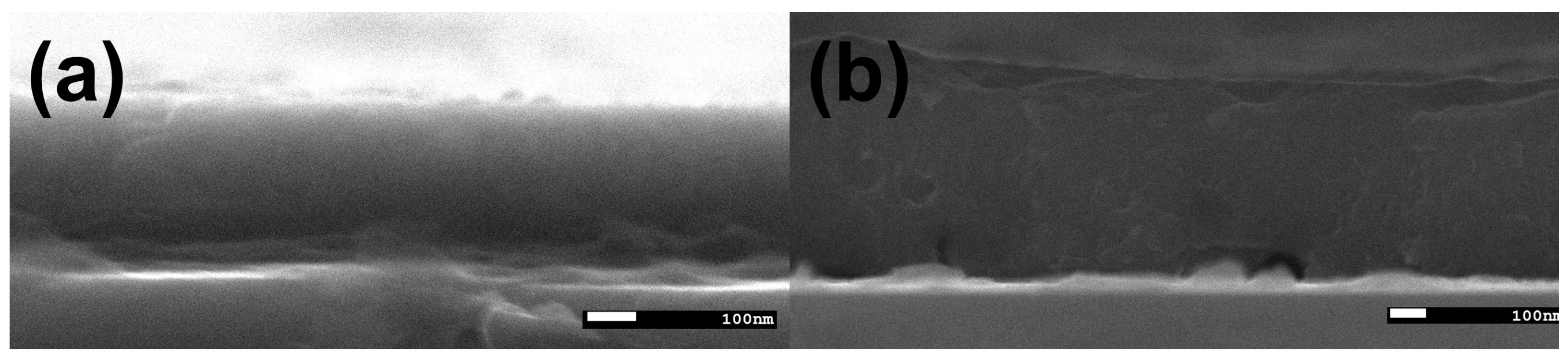
3.1. BaZrS3 Films from High Temperature Annealing

To test the plausibility of the stacked layer approach to synthesize BZS thin films, sample 1 was fabricated following the approach outlined in Figure 1b. First, 450 nm of BaS (99.9) was deposited onto silicon substrate. Subsequently, 120 nm Zr were sputtered on top. The sample was annealed alongside roughly 200 mg of elemental sulfur up to a temperature of 1100 °C. Figure 3 shows the resulting XRD pattern, while the inlet shows a macroscopic image of sample 1. The resulting film is partly ablated from the substrate. The remaining film has a rough surface on a macroscopic level. However, from the XRD pattern is indeed the desired phase BZS. There seem to be at least one secondary phases present, which was identified by the analysis software to be most likely Ba3Zr2S7. But it should be noted that the observed peaks do not exactly match the reference patterns and instead are slightly offset, meaning they might be related to other compounds. Additional phases that might have not been identified might also be present. Still, the key result is that BZS was formed during this high temperature annealing experiment with a rough film quality on a macroscopic level and the presence of secondary phases.

3.2. Improved Microstructure and Reduced Synthesis Temperature of BaS3 Films

After improving the vacuum quality of the sulfurization setup and increasing the BaS source material purity, the temperature to obtain phase pure BaS3 films was reduced from 350 °C to 300 °C. This was accommodated by in improved microstructure as can be seen from the microscope images in Figure 4. The previously published images (Figure 4a–d) of Samples 2 to 4 show large worm-like bulges (Figure 4a) and islands (Figure 4b–d). The more recently fabricated Samples 5 to 8 (Figure 4e–h) show similar features, but they appear to be on a smaller scale. The BaS3 films possess a yellowish color on a macroscopic scale, while on a microscopic scale, generally a red background and green bulges or islands can be seen. Figure 5 shows the initial BaS film as well as a sulfurized BaS3 film in top and cross-sectional views taken with an SEM. Prior to sulfurization, the BaS film is smooth (Figure 5a). After sulfurization, bulges can clearly be observed on the BaS3 film (Figure 5b). From the cross-sectional image in Figure 5d), it can be seen, that the film lifts off the substrate to form the bulges. The film also seems not to adhere well to the substrate, whereas the BaS film is firmly attached to the substrate (Figure 5c). From the cross-sectional images, the film thicknesses were determined. For this, the images in Figure 5c,d and Figure A1 were used for Samples 10 and 9, respectively. The average thickness of the BaS film was 350 ± 15 nm. This value was used to calibrate the thicknesses monitored during the BaS film deposition when using the 99.9% purity source material. The determined thickness of the BaS3 film was 618 ± 50 nm. The film therefore increased by 56.4% in thickness. The larger error for the BaS3 film is a result of the less uniform surface of the film compared to the BaS film. The areas measured with EDX and the resulting spectra are displayed in Figure A2. As expected, only the elements Si, Ba and S significantly contribute to the measurement signal. In case of BaS, the Ba:S ratio is 1:0.97, which is almost exactly the expected 1:1 ratio. For the BaS3 film, this ratio is 1:2.72. This is only slightly sulfur deficient, confirming in both cases the expected stoichiometry of the samples.

3.3. Attempts of Rapid Synthesis of BaS3 Films

To better understand the formation of the BaS3 thin film from the BaS film, experiments with shortened annealing times were conducted. By doing this, the time, after which BaS3 forms can be determined and potential intermediate states observed. Samples were annealed for 5, 10, 15 and 20 min. The previously established 30 min annealing time in an oven set to 300 °C. The latter was maintained throughout the experiment. The crystal structures of the samples were determined using XRD measurements. After 5 min annealing, no change of the sample was observed, and most of the sulfur remained in the crucible inside the graphite box. However, it appeared to have melted as it no longer was in powder form. After 10 min, the film appeared to be BaS2 based on the XRD pattern (Figure 6a). This result was unexpected based on our previously published data. There, BaS2 was obtained at higher temperatures than those to synthesize BaS3 [49]. After 15 min, BaS3 was the major constituent of the film (Figure 6b). The same was true for the sample annealed for 20 min.
During the annealing experiments, the temperatures of the sample and the inside of the oven were recorded. For samples annealed for 10 and 30 min, the resulting temperature curves are displayed in Figure 6c,d. From these curves, the temperature needed to obtain BaS3 can be determined. After 10 min of annealing the sample in the oven set to 300 °C, the sample almost reaches 300 °C. After 15 min of annealing, the sample reaches 305 °C. In the remaining 15 min of annealing, the sample and oven temperature initially continue to rise, before they fall again. At the end of the 30 min anneal, roughly 305 °C is achieved again. The rise above the oven set temperature of 300 °C is due to the oven regulation setup. After the initial cooldown, the software initiates the oven the heat up to compensate. Due to the slow heating of the oven, heating above the desired temperature is unavoidable. To obtain BaS3, either a slightly higher temperature compared to obtaining BaS2 is needed, and/or a slightly longer annealing time. To test these hypotheses, experiments using a comparatively hot preheated oven (660 °C) were conducted. In those experiments, the sample was extracted from the oven upon reaching about 300 °C. The XRD pattern for sample 16 is displayed in Figure 7 alongside its temperature curve during the annealing. Figure A3 shows the same data for three samples processed in a similar fashion, differing only slightly in the time they remained in the hot zone. For sample 16, this was done after 1:30 min, but the temperature continued to rise until it reached its maximum at 2 min of 422.3 °C. This trend was observed for the other three samples similarly (Figure A3b–d). Because of this, the annealing time between the four samples were varied slightly. Based on the XRD data, samples 17 and 18 showed the presence of small amounts of BaS2.
Figure 8 shows microscope images of some of those samples, that were rapidly thermally processed. Overall, the microstructure observed for Sample 15 (Figure 8a,b) matches those observed for previously described samples (Figure 4e,f). Samples 16 and 17 show an increased presence of defects (Figure 8c,d) compared to Sample 16.

4. Discussion

First, the possibility to produce BZS thin films from stacked layers was demonstrated. This was achieved by annealing a stack of BaS-Zr layers alongside an excess of sulfur at temperatures up to 1100 °C. However, the resulting film quality was very poor as the film partially ablated and the remaining film also was patchy (Figure 3 inlet). This could have been caused by a mismatch of the thermal expansion coefficients of the involved layers and a too rapid heating of the sample. By executing a slower heating of the oven, ablation of the film could be avoided. Besides the desired BZS phase, several secondary phases were detected. Most likely, they were the Ruddlesden-Popper phase Ba3Zr2S7 and the binary compound ZrS2. The latter could indicate, that in the process, ZrS2 forms first from the reaction of Zr and gaseous sulfur before reacting with BaS. It could therefore indicate that longer annealing might be needed to complete the process and obtain a phase pure product. Yang et al. point out that this might be due to the low reactivity of elemental Zr. As the supply of Zr is limited, the Zr-poor phase Ba3Zr2S7 forms instead of the desired perovskite [51]. In our experiments, Zr might be particularly slow to react due to air exposure of the sample during transfer to the oven. The element is known to form a layer of ZrO2 on the surface when exposed to oxygen, which is a relatively inert material. And as discussed before, Zr might only be available for the formation of the ternary compounds after being sulfurized first, which would explain the supposedly low reaction rate. It might be better to use ZrS2 or ZrS3 instead of elemental Zr in this type of process. Or to deposit Zr first and do a separate sulfurization step for it. This could be done by following the approach of Zhang et al., who annealed Zr-foil alongside elemental sulfur to initially obtain ZrS3 nanobelt quasi-arrays. To obtain ZrS2, they further annealed the ZrS3 sample [54]. This is enabled by the fact, that ZrS2 and ZrS3 can be reversibly converted to one another [47]. It should be noted, that ZrS2 can be obtained by sulfurization of ZrO2 with CS2, but high temperatures (>1200 °C) are needed, as noted by Clearfield [55]. Nonetheless, further improvements in the processing are needed to obtain high quality BZS films from such a high temperature annealing approach. Several important parameters for this approach have been identified, particularly the processing temperature progression and the choice of the Zr-precursor.
By improving the quality of the vacuum oven setup and using higher purity BaS source material, it was possible to significantly improve the morphology of the resulting films and reduce the synthesis from 350 °C to 300 °C. To understand this, multiple factors should be considered. The vacuum setup was improved by not only introducing full electronic control over all parameters, particularly pressure and gas flow, but also several leaks were patched, resulting in a lower minimum pressure in the range of 10−2 mbar compared to a minimum pressures of about 1 mbar in our previous work [49]. Firstly, this reduces the amount of oxygen and water residue present during the process. Water is particularly problematic, as it is known to react with BaS to form H2S gas and Ba(OH)2. The latter could be a source of defects in the final film. Because of this, the improved vacuum setup could be the cause of the improved BaS3 film morphology. Additionally, while the pressure was controlled to remain constant throughout the sulfurization process, it does not seem unreasonable, that there could be a pressure gradient within the tube furnace. The pressure was measured on the farthest away side from the vacuum pump, and so throughout the quartz tube there could be a pressure gradient (Figure 2). If this is the case, the reduced base pressure translates to a reduced pressure within the graphite box during the annealing. This reduces the melting and boiling points of the compounds involved, in particular sulfur evaporates at a lower temperature. This could explain, why the improved vacuum setup lead to a reduced synthesis temperature. This reduced synthesis temperature itself then could have impacted the final film morphology. It leads to less thermal stress in the film and the substrate, resulting in smaller bulges and less cracks. The influence of the source material purity is not as straightforward, but it is known that a higher purity BaS possesses a higher melting point than a less pure BaS. This resulted in a lower deposition rate of the deposited BaS film as it was significantly harder to evaporate. This presumably leads to an improved crystallinity of the initial BaS film. Due to the lower deposition rate, larger crystallites with less defects could have formed. Therefore, it was possible due to the improved vacuum oven setup and the increased BaS source material purity to improve the morphology of the final film and reduce the synthesis temperature. This development is crucial for future works, as the previously synthesized films were morphologically too poor to be considered for further processing [49].
From the experiments with reduced annealing times, it seems apparent that BaS2 serves as an intermediate in the formation of BaS3 from BaS during sulfurization. However, this is in contradiction to our previous results, were BaS2 was observed at higher annealing temperatures than those to obtain BaS3 [49]. This might be explained the following way: At a higher temperature, the S evaporates quicker and is consumed before the formation of BaS3 is completed. In this context it should be noted that the graphite box used for the sulfurization is not perfectly sealed, so sulfur vapors can escape from it during the process. In order to obtain BaS3, a certain temperature needs to be achieved, and enough sulfur needs to be supplied or a high enough sulfur partial pressure need to be maintained to finish the reaction. Yang. et al. showed that BaS3 can decompose to BaS2 and that this reaction is slow, so it seems reasonable, that the reverse reaction is possible and is relatively fast [51]. BaS2 was formed after 10 min, whereas BaS3 was formed after 15 min (Figure 6). From this information and the temperature curves obtained from the annealing experiments, it was possible to determine, that temperatures in the range of 305 °C are needed to obtain BaS3. Based on this, rapid annealing experiments were attempted. In those, the oven was maintained at a relatively high temperature of 660 °C and samples were only maintained in the hot zone for short periods between one and two minutes. Samples annealed for the shortest times of 1:10 min and 1:25 contained trace amounts of BaS2 (Figure A3), further indicating, that BaS2 acts as an intermediate for BaS3. Notably, the samples annealed for 1:30 min and 2 min did not show any secondary phases in the XRD. They also reached significantly higher maximum temperatures. It seems then that the parameters used for those experiments were right on the edge to obtain BaS3 thin films. The sample temperature seemingly continued to rise after the sample was removed from the hot zone. Most likely, this is just a delayed signal. The graphite box gets heated in the vacuum oven, but it takes a bit of time before the sample holder and therefore the thermocouple reaches the same temperature. The samples processed rapidly possess a comparable microstructure to those annealed for 30 min at 300 °C (Figure 4e–h and Figure 8). This leads to the conclusion, that the attempts to significantly reduce the BaS3 thin film sulfurization time were successful. Future work now needs to focus on selecting a suitable Zr-source to combine with the BaS3 films to successfully fabricate BZS films.
In summary, this work showcases two approaches for the synthesis of BZS thin films based on stacked layers. The first uses high temperatures (1100 °C) and stacked layers of BaS-Zr. It was demonstrated, that BZS films can be synthesized in this manner. However, the resulting morphology was very poor and further improvements to the process need to be done to successfully fabricate high quality films in this fashion. The second approach aims to utilize the low melting phase BaS3 in the synthesis of BZS. By improving the vacuum in the oven used for the sulfurization of BaS films and using higher purity BaS source material, the film morphology was significantly improved compared to previously published results. Furthermore, the annealing temperature to obtain BaS3 was reduced from 350 °C to about 300 °C. From varying the annealing time between 5 and 30 min, it was possible to identify BaS2 as an intermediate during the sulfurization of BaS films. The temperature needed to obtain BaS3 was determined to be 305 °C during the annealing process used in this work. From this, a rapid annealing approach was developed. When the sulfurization was conducted at 660 °C, phase pure BaS3 films were obtained after only 1:30 min of annealing. This study lays the groundwork to produce BZS from stacked layers in future research. Particularly, more studies focused on the successful combination of the improved BaS3 layer with a Zr-source layer need to be conducted.

Author Contributions

Conceptualization, T.F. and P.W., methodology, T.F. and P.W.; validation, T.F., S.J. and M.M.; formal analysis, T.F., investigation, T.F., S.J. and M.M; resources, P.W.; data curation,T.F.; writing—original draft preparation, T.F.; writing—review and editing, S.J. and P.W.; visualization, T.F.; supervision, P.W.; project administration, P.W.; funding acquisition, P.W. All authors have read and agreed to the published version of the manuscript.

Funding

This research was funded by the “Deutsche Forschungsgemeinschaft”, IGK 2495/I.

Data Availability Statement

The original contributions presented in the study are included in the article; further inquiries can be directed to the corresponding author.

Conflicts of Interest

The authors declare no conflict of interest. The funders had no role in the design of the study; in the collection, analyses, or interpretation of data; in the writing of the manuscript; or in the decision to publish the results.

Appendix A

Figure A1. BaS film (Sample 10, (a)) and BaS3 film (Sample 9, (b)) cross-sections additionally used for the determination of the film thicknesses.
Crystals 14 00267 g0a1
Figure A2. Areas used for EDX measurements (a,b) and the resulting spectra (c,d) for a BaS film (Sample 10, (a,c)) and a BaS3 film (Sample 9, (b,d)).
Crystals 14 00267 g0a2
Figure A3. XRD patterns of BaS3 Samples 15, 17 and 18 annealed in the rapid processing route (a) and their respective temperature curves with the sample temperature in blue and the oven temperature in orange (bd).
Crystals 14 00267 g0a3

References

  1. Swarnkar, A.; Mir, W.J.; Chakraborty, R.; Jagadeeswararao, M.; Sheikh, T.; Nag, A. Are Chalcogenide Perovskites an Emerging Class of Semiconductors for Optoelectronic Properties and Solar Cell? Chem. Mater. 2019, 31, 565–575. [Google Scholar] [CrossRef]
  2. Sun, Y.Y.; Agiorgousis, M.L.; Zhang, P.; Zhang, S. Chalcogenide perovskites for photovoltaics. Nano Lett. 2015, 15, 581–585. [Google Scholar] [CrossRef] [PubMed]
  3. Sopiha, K.V.; Comparotto, C.; Márquez, J.A.; Scragg, J.J.S. Chalcogenide Perovskites: Tantalizing Prospects, Challenging Materials. Adv. Opt. Mater. 2021, 10, 2101704. [Google Scholar] [CrossRef]
  4. Ye, K.; Koocher, N.Z.; Filippone, S.; Niu, S.; Zhao, B.; Yeung, M.; Bone, S.; Robinson, A.J.; Vora, P.; Schleife, A.; et al. Low-energy electronic structure of perovskite and Ruddlesden-Popper semiconductors in the Ba-Zr-S system probed by bond-selective polarized x-ray absorption spectroscopy, infrared reflectivity, and Raman scattering. Phys. Rev. B 2022, 105, 195203. [Google Scholar] [CrossRef]
  5. Ye, K.; Zhao, B.; Diroll, B.T.; Ravichandran, J.; Jaramillo, R. Time-resolved photoluminescence studies of perovskite chalcogenides. Faraday Discuss 2022, 239, 146–159. [Google Scholar] [CrossRef] [PubMed]
  6. Surendran, M.; Chen, H.; Zhao, B.; Thind, A.S.; Singh, S.; Orvis, T.; Zhao, H.; Han, J.-K.; Htoon, H.; Kawasaki, M.; et al. Epitaxial Thin Films of a Chalcogenide Perovskite. Chem. Mater. 2021, 33, 7457–7464. [Google Scholar] [CrossRef]
  7. Liang, Y.; Zhang, Y.; Xu, J.; Ma, J.; Jiang, H.; Li, X.; Zhang, B.; Chen, X.; Tian, Y.; Han, Y.; et al. Parametric study on controllable growth of SrZrS3 thin films with good conductivity for photodetectors. Nano Res. 2023, 16, 7867–7873. [Google Scholar] [CrossRef]
  8. Marquez, J.A.; Rusu, M.; Hempel, H.; Ahmet, I.Y.; Kolbach, M.; Simsek, I.; Choubrac, L.; Gurieva, G.; Gunder, R.; Schorr, S.; et al. BaZrS3 Chalcogenide Perovskite Thin Films by H2S Sulfurization of Oxide Precursors. J. Phys. Chem. Lett. 2021, 12, 2148–2153. [Google Scholar] [CrossRef]
  9. Shaili, H.; Beraich, M.; El hat, A.; Ouafi, M.; Salmani, E.M.; Essajai, R.; Battal, W.; Rouchdi, M.; Taibi, M.H.; Hassanain, N.; et al. Synthesis of the Sn-based CaSnS3 chalcogenide perovskite thin film as a highly stable photoabsorber for optoelectronic applications. J. Alloys Compd. 2021, 851, 156790. [Google Scholar] [CrossRef]
  10. Yu, Z.; Deng, C.; Kong, S.; Hui, H.; Guo, J.; Zhao, Q.; Tian, F.; Zhou, C.; Zhang, Y.; Yang, S.; et al. Transition Metal-Doped Chalcogenide Perovskite Magnetic Semiconductor BaZrS3. SSRN Electron. J. 2022, 563, 169886. [Google Scholar] [CrossRef]
  11. Pandey, J.; Ghoshal, D.; Dey, D.; Gupta, T.; Taraphder, A.; Koratkar, N.; Soni, A. Local ferroelectric polarization in antiferroelectric chalcogenide perovskite BaZrS3 thin films. Phys. Rev. B 2020, 102, 205308. [Google Scholar] [CrossRef]
  12. Gupta, T.; Ghoshal, D.; Yoshimura, A.; Basu, S.; Chow, P.K.; Lakhnot, A.S.; Pandey, J.; Warrender, J.M.; Efstathiadis, H.; Soni, A.; et al. An Environmentally Stable and Lead-Free Chalcogenide Perovskite. Adv. Funct. Mater. 2020, 30, 2001387. [Google Scholar] [CrossRef]
  13. Hahn, H.; Mutschke, U. Untersuchungen über ternäre Chalkogenide. XI. Versuche zur Darstellung von Thioperowskiten. Z. Für Anorg. Und Allg. Chem. 1957, 288, 269–278. [Google Scholar] [CrossRef]
  14. Wang, Y.; Sato, N.; Yamada, K.; Fujino, T. Synthesis of BaZrS3 in the presence of excess sulfur. J. Alloys Compd. 2000, 311, 214–223. [Google Scholar] [CrossRef]
  15. Wang, Y.; Sato, N.; Fujino, T. Synthesis of BaZrS3 by short time reaction at lower temperatures. J. Alloys Compd. 2001, 327, 104–112. [Google Scholar] [CrossRef]
  16. Niu, S.; Huyan, H.; Liu, Y.; Yeung, M.; Ye, K.; Blankemeier, L.; Orvis, T.; Sarkar, D.; Singh, D.J.; Kapadia, R.; et al. Bandgap Control via Structural and Chemical Tuning of Transition Metal Perovskite Chalcogenides. Adv. Mater. 2017, 29, 1604733. [Google Scholar] [CrossRef] [PubMed]
  17. Niu, S.; Milam-Guerrero, J.; Zhou, Y.; Ye, K.; Zhao, B.; Melot, B.C.; Ravichandran, J. Thermal stability study of transition metal perovskite sulfides. J. Mater. Res. 2018, 33, 4135–4143. [Google Scholar] [CrossRef]
  18. Niu, S.; Zhao, B.; Ye, K.; Bianco, E.; Zhou, J.; McConney, M.E.; Settens, C.; Haiges, R.; Jaramillo, R.; Ravichandran, J. Crystal growth and structural analysis of perovskite chalcogenide BaZrS3 and Ruddlesden–Popper phase Ba3Zr2S7. J. Mater. Res. 2019, 34, 3819–3826. [Google Scholar] [CrossRef]
  19. Clearfield, A. The synthesis and crystal structures of some alkaline earth titanium and zirconium sulfides. Acta Crystallogr. 1963, 16, 135–142. [Google Scholar] [CrossRef]
  20. Nitta, T.; Nagase, K.; Hayakawa, S. Formation, Microstructure, and Properties of Barium Zirconium Sulfide Ceramics. J. Am. Ceram. Soc. 1970, 53, 601–604. [Google Scholar] [CrossRef]
  21. Lelieveld, R.; Ijdo, D.J.W. Sulphides with the GdFeO3 structure. Acta Crystallogr. Sect. B Struct. Crystallogr. Cryst. Chem. 1980, 36, 2223–2226. [Google Scholar] [CrossRef]
  22. Bystricky, R.; Tiwari, S.K.; Hutar, P.; Vanco, L.; Sykora, M. Synthesis of Sulfide Perovskites by Sulfurization with Boron Sulfides. Inorg. Chem. 2022, 61, 18823–18827. [Google Scholar] [CrossRef]
  23. Gross, N.; Sun, Y.-Y.; Perera, S.; Hui, H.; Wei, X.; Zhang, S.; Zeng, H.; Weinstein, B.A. Stability and Band-Gap Tuning of the Chalcogenide Perovskite BaZrS3 in Raman and Optical Investigations at High Pressures. Phys. Rev. Appl. 2017, 8, 044014. [Google Scholar] [CrossRef]
  24. Wei, X.; Hui, H.; Perera, S.; Sheng, A.; Watson, D.F.; Sun, Y.Y.; Jia, Q.; Zhang, S.; Zeng, H. Ti-Alloying of BaZrS3 Chalcogenide Perovskite for Photovoltaics. ACS Omega 2020, 5, 18579–18583. [Google Scholar] [CrossRef]
  25. Ramanandan, S.P.; Giunto, A.; Stutz, E.Z.; Reynier, B.; Lefevre, I.T.F.M.; Rusu, M.; Schorr, S.; Unold, T.; Morral, A.F.I.; Márquez, J.A.; et al. Understanding the growth mechanism of BaZrS3 chalcogenide perovskite thin films from sulfurized oxide precursors. J. Phys. Energy 2022, 5, 014013. [Google Scholar] [CrossRef]
  26. Sharma, S.; Ward, Z.; Bhimani, K.; Li, K.; Lakhnot, A.; Jain, R.; Shi, S.-F.; Terrones, H.; Koratkar, N. Bandgap Tuning in BaZrS3 Perovskite Thin Films. ACS Appl. Electron. Mater. 2021, 3, 3306–3312. [Google Scholar] [CrossRef]
  27. Sharma, S.; Ward, Z.D.; Bhimani, K.; Sharma, M.; Quinton, J.; Rhone, T.D.; Shi, S.F.; Terrones, H.; Koratkar, N. Machine Learning-Aided Band Gap Engineering of BaZrS3 Chalcogenide Perovskite. ACS Appl. Mater. Interfaces 2023, 15, 18962–18972. [Google Scholar] [CrossRef] [PubMed]
  28. Comparotto, C.; Davydova, A.; Ericson, T.; Riekehr, L.; Moro, M.V.; Kubart, T.; Scragg, J. Chalcogenide Perovskite BaZrS3: Thin Film Growth by Sputtering and Rapid Thermal Processing. ACS Appl. Energy Mater. 2020, 3, 2762–2770. [Google Scholar] [CrossRef]
  29. Comparotto, C.; Ström, P.; Donzel-Gargand, O.; Kubart, T.; Scragg, J.J.S. Synthesis of BaZrS3 Perovskite Thin Films at a Moderate Temperature on Conductive Substrates. ACS Appl. Energy Mater. 2022, 5, 6335–6343. [Google Scholar] [CrossRef]
  30. Sadeghi, I.; Ye, K.; Xu, M.; Li, Y.; LeBeau, J.M.; Jaramillo, R. Making BaZrS3 Chalcogenide Perovskite Thin Films by Molecular Beam Epitaxy. Adv. Funct. Mater. 2021, 31, 2105563. [Google Scholar] [CrossRef]
  31. Sadeghi, I.; Sambeek, J.V.; Simonian, T.; Ye, K.; Nicolosi, V.; LeBeau, J.M.; Jaramillo, R. A new semiconducting perovskite alloy system made possible by gas-source molecular beam epitaxy. arXiv 2022, arXiv:2211.10787. [Google Scholar]
  32. Surendran, M.; Zhao, B.; Ren, G.; Singh, S.; Avishai, A.; Chen, H.; Han, J.-K.; Kawasaki, M.; Mishra, R.; Ravichandran, J. Quasi-epitaxial growth of BaTiS3 films. J. Mater. Res. 2022, 37, 3481–3490. [Google Scholar] [CrossRef]
  33. Ravi, V.K.; Yu, S.H.; Rajput, P.K.; Nayak, C.; Bhattacharyya, D.; Chung, D.S.; Nag, A. Colloidal BaZrS3 Chalcogenide Perovskite Nanocrystals for Thin Film Device Fabrication. Nanoscale 2021, 13, 1616–1623. [Google Scholar] [CrossRef]
  34. Dhole, S.; Wei, X.; Hui, H.; Roy, P.; Corey, Z.; Wang, Y.; Nie, W.; Chen, A.; Zeng, H.; Jia, Q. A Facile Aqueous Solution Route for the Growth of Chalcogenide Perovskite BaZrS3 Films. Photonics 2023, 10, 366. [Google Scholar] [CrossRef]
  35. Turnley, J.W.; Vincent, K.C.; Pradhan, A.A.; Panicker, I.; Swope, R.; Uible, M.C.; Bart, S.C.; Agrawal, R. Solution Deposition for Chalcogenide Perovskites: A Low-Temperature Route to BaMS3 Materials (M = Ti, Zr, Hf). J. Am. Chem. Soc. 2022, 144, 18234–18239. [Google Scholar] [CrossRef]
  36. Pradhan, A.A.; Uible, M.C.; Agarwal, S.; Turnley, J.W.; Khandelwal, S.; Peterson, J.M.; Blach, D.D.; Swope, R.N.; Huang, L.; Bart, S.C.; et al. Synthesis of BaZrS3 and BaHfS3 Chalcogenide Perovskite Films Using Single-Phase Molecular Precursors at Moderate Temperatures. Angew. Chem. Int. Ed. 2023, 62, e202301049. [Google Scholar] [CrossRef]
  37. Nwambaekwe, K.C.; John-Denk, V.S.; Douman, S.F.; Mathumba, P.; Yussuf, S.T.; Uhuo, O.V.; Ekwere, P.I.; Iwuoha, E.I. Crystal engineering and thin-film deposition strategies towards improving the performance of kesterite photovoltaic cell. J. Mater. Res. Technol. 2021, 12, 1252–1287. [Google Scholar] [CrossRef]
  38. Künecke, U.; Hetzner, C.; Möckel, S.; Yoo, H.; Hock, R.; Wellmann, P. Characterization of kesterite thin films fabricated by rapid thermal processing of stacked elemental layers using spatially resolved cathodoluminescence. Thin Solid Film. 2015, 582, 387–391. [Google Scholar] [CrossRef]
  39. Powalla, M.; Paetel, S.; Hariskos, D.; Wuerz, R.; Kessler, F.; Lechner, P.; Wischmann, W.; Friedlmeier, T.M. Advances in Cost-Efficient Thin-Film Photovoltaics Based on Cu(In,Ga)Se2. Engineering 2017, 3, 445–451. [Google Scholar] [CrossRef]
  40. Ramanujam, J.; Singh, U.P. Copper indium gallium selenide based solar cells—A review. Energy Environ. Sci. 2017, 10, 1306–1319. [Google Scholar] [CrossRef]
  41. Hossain, E.S.; Chelvanathan, P.; Shahahmadi, S.A.; Bais, B.; Akhtaruzzaman, M.; Tiong, S.K.; Sopian, K.; Amin, N. Fabrication of Cu2SnS3 thin film solar cells by sulphurization of sequentially sputtered Sn/CuSn metallic stacked precursors. Sol. Energy 2019, 177, 262–273. [Google Scholar] [CrossRef]
  42. Wibowo, R.A.; Moeckel, S.; Yoo, H.; Hoelzing, A.; Hock, R.; Wellmann, P.J. Formation of Cu2SnSe3 from stacked elemental layers investigated by combined In Situ X-ray diffraction and differential scanning calorimetry techniques. J. Alloys Compd. 2014, 588, 254–258. [Google Scholar] [CrossRef]
  43. Jung, G.S.; Mun, S.H.; Shin, D.; Chalapathy, R.B.V.; Ahn, B.T.; Kwon, H. Fabrication of a smooth, large-grained Cu(In,Ga)Se2 thin film using a Cu/(In,Ga)2Se3 stacked precursor at low temperature for CIGS solar cells. RSC Adv. 2015, 5, 7611–7618. [Google Scholar] [CrossRef]
  44. Massalski, T.B.; Okamoto, H.; Subramanian, P.R.; Kacprzak, L. (Eds.) Binary Alloy Phase Diagrams, 2nd ed.; ASM International: Materials Park, OH, USA, 1990. [Google Scholar]
  45. Kresse, R.; Baudis, U.; Jäger, P.; Riechers, H.H.; Wagner, H.; Winkler, J.; Wolf, H.U. Barium and Barium Compounds. In Ullmann’s Encyclopedia of Industrial Chemistry; Wiley: Hoboken, NJ, USA, 2007. [Google Scholar]
  46. Nielsen, R.H.; Wilfing, G. Zirconium and Zirconium Compounds. In Ullmann’s Encyclopedia of Industrial Chemistry; Wiley: Hoboken, NJ, USA, 2010. [Google Scholar]
  47. Dang, V.Q.; Al-Ali, K. The synthesis and investigation of the reversible conversion of layered ZrS2 and ZrS3. New J. Chem. 2020, 44, 7583–7590. [Google Scholar] [CrossRef]
  48. Steudel, R. Liquid Sulfur. In Elemental Sulfur and Sulfur-Rich Compounds I; Springer: Berlin/Heidelberg, Germany, 2003; pp. 81–116. [Google Scholar]
  49. Freund, T.; Cicconi, M.R.; Wellmann, P.J. Fabrication of Bariumtrisulphide Thin Films as Precursors for Chalcogenide Perovskites. Phys. Status Solidi B 2022, 259, 2200094. [Google Scholar] [CrossRef]
  50. Yang, R.; Jess, A.D.; Fai, C.; Hages, C.J. Low-Temperature, Solution-Based Synthesis of Luminescent Chalcogenide Perovskite BaZrS3 Nanoparticles. J. Am. Chem. Soc. 2022, 144, 15928–15931. [Google Scholar] [CrossRef]
  51. Yang, R.; Nelson, J.; Fai, C.; Yetkin, H.A.; Werner, C.; Tervil, M.; Jess, A.D.; Dale, P.J.; Hages, C.J. A Low-Temperature Growth Mechanism for Chalcogenide Perovskites. Chem. Mater. 2023, 35, 4743–4750. [Google Scholar] [CrossRef]
  52. Vincent, K.C.; Agarwal, S.; Turnley, J.W.; Agrawal, R. Liquid Flux–Assisted Mechanism for Modest Temperature Synthesis of Large-Grain BaZrS3 and BaHfS3 Chalcogenide Perovskites. Adv. Energy Sustain. Res. 2023, 4, 2300010. [Google Scholar] [CrossRef]
  53. Kollmuss, M.; La Via, F.; Wellmann, P.J. Effect of Growth Conditions on the Surface Morphology and Defect Density of CS-PVT-Grown 3C-SiC. Cryst. Res. Technol. 2023, 58, 2300034. [Google Scholar] [CrossRef]
  54. Zhang, Y.L.; Wu, X.C.; Tao, Y.R.; Mao, C.J.; Zhu, J.J. Fabrication and field-emission performance of zirconium disulfide nanobelt arrays. Chem. Commun. 2008, 2683–2685. [Google Scholar] [CrossRef]
  55. Clearfield, A. The Synthesis and Properties of Zirconium Disulfide. J. Am. Chem. Soc. 1958, 80, 6511–6513. [Google Scholar] [CrossRef]
Figure 1. Schematic illustration showing the general approach of stacked layers (a), the high temperature approach (b) and the BaS3 based approach (c).
Crystals 14 00267 g001
Figure 2. Schematic of the oven setup used for sulfurization showing the positions of the various instruments.
Crystals 14 00267 g002
Figure 3. XRD of Sample 1 annealed at high temperature (1100 °C) showing a match with BZS and other secondary phases. The inlet is a macroscopic image of the same sample showing the ablated parts and the sub-optimal surface structure.
Crystals 14 00267 g003
Figure 4. Comparison of microscope images of previously fabricated BaS3 samples ((ad), reused with permission from [49]) and BaS3 samples fabricated as part of this study (eh). The microstructures of Samples 2 (a), 3 (b) and 4 (c,d) have larger defects and bulges than Samples 5 (e), 6 (f), 7 (g) and 8 (h). The different colors in (eh) are not accurate to reality and are caused by differences in the white balance.
Crystals 14 00267 g004
Figure 5. SEM images of Sample 10 (a,c) and Sample 9 (b,d) showing the surface of BaS and BaS3 films, respectively, in top (a,b) and cross-sectional (c,d) view.
Crystals 14 00267 g005
Figure 6. The XRD pattern (black) of Sample 12 annealed for 10 min shows a good match with the BaS2 reference pattern in red (a), whereas Sample 13 annealed for 15 min matches with BaS3 (b). The Temperature curves for Samples 12 and 9 annealed for 10 (c) and 30 min (d), respectively, demonstrate, that a temperature slightly above 300 °C is needed to obtain a BaS3 film. The sample temperatures are displayed in blue, whereas the oven temperature is displayed in orange.
Crystals 14 00267 g006
Figure 7. (a) XRD spectrum of Sample 16 annealed in rapid thermal processing, showing good match with the BaS3 reference pattern (red lines). (b) Temperature curve for the same sample (blue line) showing the rise in temperature up to 420 °C even after exertion of the sample after 1:30 min. The oven temperature (orange line) was set to 660 °C and only slightly drops during the process.
Crystals 14 00267 g007
Figure 8. The microscope images of rapidly annealed BaS3 film samples show a similar microstructure to those annealed for 30 min. (a,b) show Sample 15, (c,d) show Samples 16 and 17, respectively.
Crystals 14 00267 g008
Table 1. BaS Film Deposition Parameters.
Sample Nr.BaS Film Thickness [nm].SubstrateBaS Purity [%].
1350Si99.9
2440Glass99.7
3180Glass99.7
4 *970Glass99.7
5400Glass99.9
6235Glass99.9
7235Glass99.9
8235Glass99.9
9395Si99.9
10350Si99.9
11~400Glass99.9
12~400Glass99.9
13~400Glass99.9
14~400Glass99.9
15415Glass99.9
16415Glass99.9
17415Glass99.9
18415Glass99.9
* BaS Film Deposition was done in two subsequent instances.
Table 2. Parameters of the annealing to sulfurize the BaS Films to form BaS3.
Sample NrSet Temperature [°C].Annealing Time [min].Pressure [mbar].Sulfur Amount [mg].
2350302.750
3350301.3100
4350301.3104
5300331066
630030~0.04 174
7300301064
83003035 281
9300301074
11300510~80
123001010~80
133001510~80
143002010~80
15660210110
166601:301080
176601:2510 3106
186601:1010 484
1 No N2 flow was applied during the duration of the experiment. 2 500 sccm N2 flow was applied during this experiment. 3 50 sccm N2 flow was applied during this experiment. 4 40 sccm N2 flow was applied during this experiment.
Disclaimer/Publisher’s Note: The statements, opinions and data contained in all publications are solely those of the individual author(s) and contributor(s) and not of MDPI and/or the editor(s). MDPI and/or the editor(s) disclaim responsibility for any injury to people or property resulting from any ideas, methods, instructions or products referred to in the content.

