1. Introduction
The 2D-TMDs have attracted considerable attention in optoelectronics, electronics, and spintronics due to their distinctive physical properties. The properties of interest in this context encompass the atomic thinness geometry of the material, layer-dependent valley polarization, tunable spin [
1,
2,
3] and optoelectronic [
4,
5,
6] and electronic properties [
7,
8,
9]. However, much of the existing research has been limited to mechanically exfoliated two-dimensional materials, which have inherent limitations in terms of output and size. Consequently, developing strategies for large-area single-layer TMD preparation is crucial for practical applications. Currently, synthetic approaches for producing high-quality large-area TMDs include organic metal gas-source CVD (MOCVD) [
10,
11] and solid-source chemical vapor deposition (CVD) [
12,
13,
14]. Solid-source CVD offers advantages such as larger crystals and reduced doping and contamination from organometallic precursors, resulting in higher crystal quality for produced two-dimensional materials. Solid-source CVD methods have also recently achieved wafer-level growth of polycrystalline two-dimensional crystals [
15,
16]. Despite significant progress, materials synthesized through current strategies often exhibit issues such as uneven thickness, restricted dimensions of single crystal domains, or sluggish growth rates. Planting large single-crystal domains devoid of grain boundaries guarantees superior electronic performance and device yield across a wide expanse. This factor ultimately plays a decisive role in practically applying two-dimensional materials in electronic and optoelectronic devices. Minimizing the nucleation density throughout the growth procedure is imperative to produce two-dimensional materials featuring extensive single-crystal domains. The aforementioned objective can be accomplished through diverse techniques, including but not limited to maintaining a suitably limited quantity of gas-phase sources, reducing the occurrence of crystal nucleation, and impeding the development of multiple strata.
Nevertheless, these techniques generally yield a reduced lateral growth rate, frequently attaining 1 μm/s or lower [
17]. The attainment of sizable individual crystals typically necessitates prolonging the growth duration, which may span multiple hours or more to yield single-layer crystals measuring in the millimeter range. Optimizing the lateral expansion rate while minimizing the vertical expansion rate is a crucial determinant in the growth dynamics of two-dimensional crystals. As an illustration, a specifically tailored chemical vapor deposition (CVD) technique has notably augmented the lateral growth velocity of monolayer graphene to a maximum of 200 μm/s [
18]. In contrast to graphene, the synthesis conditions for TMD materials are more intricate, posing a challenge to the rapid growth of large single-crystal TMDs, which remains a relatively unexplored area of research [
19,
20,
21,
22,
23].
To attain swift expansion of sizable singular crystals, it is typically necessary to ensure a satisfactory abundance of precursor materials and a proportional rate of precursor surface migration [
9,
18,
24,
25]. In the given circumstances, the precursor can promptly diffuse and adhere to the periphery of the developing crystal subsequent to forming a solitary-layer nucleus, thereby impeding the formation of a fresh nucleus. To attain this objective, it is customary to employ elevated temperatures to guarantee an adequate source supply and a high rate of atomic surface diffusion [
26,
27,
28]. However, achieving TMDs with optimal characteristics necessitates precise control of growth parameters. Temperature, for instance, is a fundamental factor influencing growth kinetics and crystal structure, with specific temperature ranges tailored to different TMDs facilitating precursor diffusion and enhancing crystalline quality [
29,
30]. Precursor flow rate governs the supply of source materials, impacting growth kinetics and thickness uniformity. Maintaining an optimal flow rate is crucial to avoid excessive precursor decomposition or limited source availability, ensuring controlled growth and the required thickness [
18,
24,
25]. Additionally, growth time significantly affects the extent of TMD formation and crystal size, with longer durations promoting complete precursor conversion and yielding larger crystals. However, extended growth times may also introduce defects and impurities, necessitating a balance between growth duration and material quality [
13,
14]. The amount of material utilized in the growth process is crucial in ascertaining the dimensions and thickness of TMD materials [
16,
29]. Precursor concentration directly affects the nucleation density and growth rates, with higher concentrations leading to denser nucleation and faster growth, resulting in larger and thicker TMD crystals. However, excessively high precursor concentrations may lead to non-uniform growth and undesired phase formation. Additionally, the direction of gas flow during growth influences precursor distribution and crystal morphology [
31].
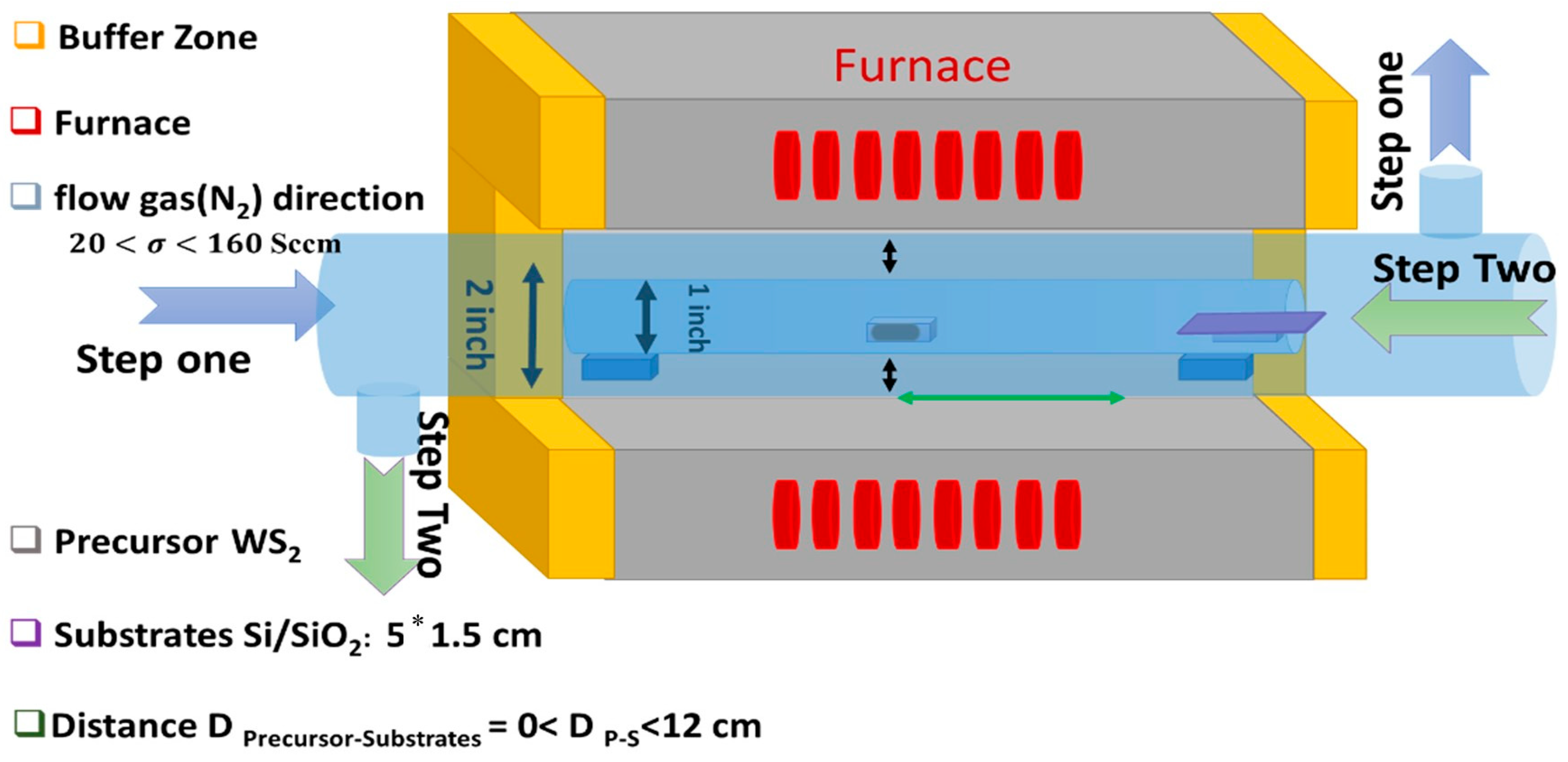
Careful control of these fundamental factors, including temperature, flow, time of growth, amount of material, and the direction of gas flow, is essential to obtain TMD materials with superior quality and desirable sizes (
Supporting Documents Scheme of Experiments Figure S1). These factors govern growth kinetics, precursor diffusion, crystalline quality, thickness uniformity, and crystal morphology. Researchers synthesizing and growing high-quality TMDs can benefit from the comprehensive insights and guidelines this research provides, enabling them to achieve optimal growth conditions. This knowledge will contribute to advancing the field of TMD synthesis and facilitating the development of novel applications that leverage the unique properties of these materials.
3. Results and Discussion
Investigating the basic conditions for growth to obtain good-quality materials is paramount in scientific research and technological advancements. Understanding and controlling the growth parameters play a significant part in deciding the properties and performance of various materials. Researchers can optimize the synthesis process and achieve materials with desirable qualities by systematically studying fundamental factors such as temperature, precursor flow, growth duration, and material quantity. This investigation enables the identification of the optimal growth conditions that lead to improved crystallinity, reduced defects, enhanced uniformity, and superior functional properties.
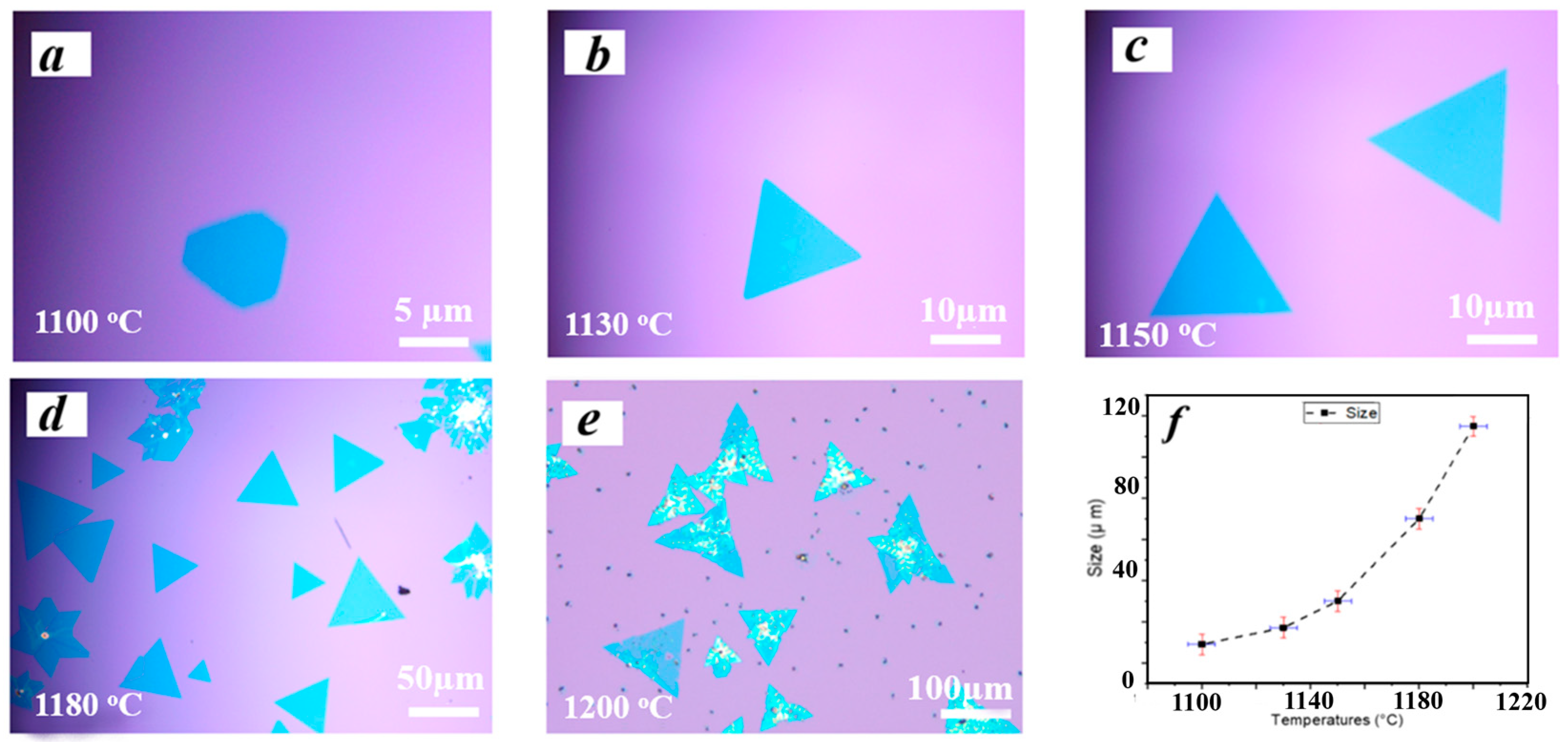
3.1. Temperature of Growth
The present study aimed to evaluate the impact of growth temperature on the crystalline properties of WS
2 film. A sequence of trials was carried out by altering the temperature of the furnace to 1100 °C, 1130 °C, 1150 °C, 1180 °C, and 1200 °C. As illustrated in
Figure 2, the average domain size of WS
2 films exhibited an initial increase, followed by a subsequent decrease as the temperature increased. The reduction in temperature led to a decline in the precursor’s diffusion rate, making it easier for the precursor to be trapped at pre-growth sites on the substrate. During the initial stages of nucleation, a significant proportion of the nucleation sites formed display the emergence of trap centers. The following precursor then triggers the process of nucleation at the trapping sites mentioned earlier, as illustrated in
Figure 2e. Consequently, a plethora of WS
2 domains that display spot-like features was acquired. The elevated temperature hindered the formation of new phases by causing an escalation in the critical nucleus radius and nucleation-free energy barrier. Consequently, the nucleation and deposition of WS
2 on the substrate were impeded. Consequently, there was a reduction in the density of nucleation. Simultaneously, a notable augmentation in the molecular thermal kinetic energy occurred, thereby promoting the surface diffusion of WO3-x and its ensuing reaction with S [
25]. The abovementioned observation is consistent with the improved crystallization of WS
2 lattices and augmented flake dimensions, as depicted in
Figure 2a–d.
Nevertheless, upon increasing the growth temperature to 1200 °C, the flake exhibited no significant increase in its dimensions. Rather, a slight reduction was noted. Furthermore, certain flakes exhibited fissures during their developmental stages, as depicted in
Figure 2e. The hypothesis suggests that the appearance of protrusion can be attributed to grain boundaries or defects, where the chemical bonding is comparatively weak and susceptible to fracture under elevated temperature conditions. Temperature is paramount in forming TMDs in two distinct respects [
32]. The temperature within the source zone is a critical variable, as even slight temperature variations can result in notable alterations in the saturation pressure of gasified solid precursors. The phenomenon above can significantly impact the process of synthesizing TMDs. The temperature can significantly influence the reaction rate in the reaction zone, as it is critical in modifying the mass transfer and reaction kinetics at the vapor–solid interface. The development of TMDs involves the conversion of solid precursors, such as sulfur and selenium, into a gaseous state through gasification. This process is achieved by utilizing the temperature present in the source zone. If the condition mentioned earlier is met, a rise in temperature results in an elevated gas concentration. Moreover, if a sufficient quantity of precursors is available, the pace of growth can be regulated by the velocity of the chemical reaction.
On the contrary, a relatively low temperature would result in a growth mechanism restricted by its ability to transfer mass. Furthermore, the progressive reduction in solid precursor levels occurs in the gaseous phase during consumption. The growth of TMDs results in a gradient of precursor feed, which presents difficulties in controlling physical vapor deposition (PVD) growth. Within the domain of nucleation events occurring at the interface between a solid and vapor, it is often noted that higher temperatures initiate a thermodynamic process. In comparison, lower temperatures initiate a kinetic process. This distinction arises from the fact that a thermodynamic process necessitates greater energy. According to recent experimental results, multilayer WSe2 nucleation occurs at temperatures surpassing 1150 °C [
33]. The current findings suggest that the number of layers detected in two-dimensional materials is notably impacted by temperature [
30,
34]. As a result, it is not unexpected that an increase in temperature during cultivation at this interface would increase the growth rate. Considerable investigation has been carried out on the influence of growth temperature on the dimensions of layers, the number of layers, and the morphology of as-synthesized WS
2 flakes, including our prior research [
31]. The current investigation highlights the significance of temperature in the controlled TMDs.
To summarize, the temperature of a physical vapor deposition (PVD) system can affect the flow of carrier gas, the chemical reactions that occur among precursors in the gas phase, and the rate at which products are deposited onto the substrate. The aforementioned traits imply that temperature can affect the merchandise’s composition and uniformity. High-quality products are often attainable at elevated temperatures, albeit at a significant energy cost and with a restricted selection of appropriate substrates.
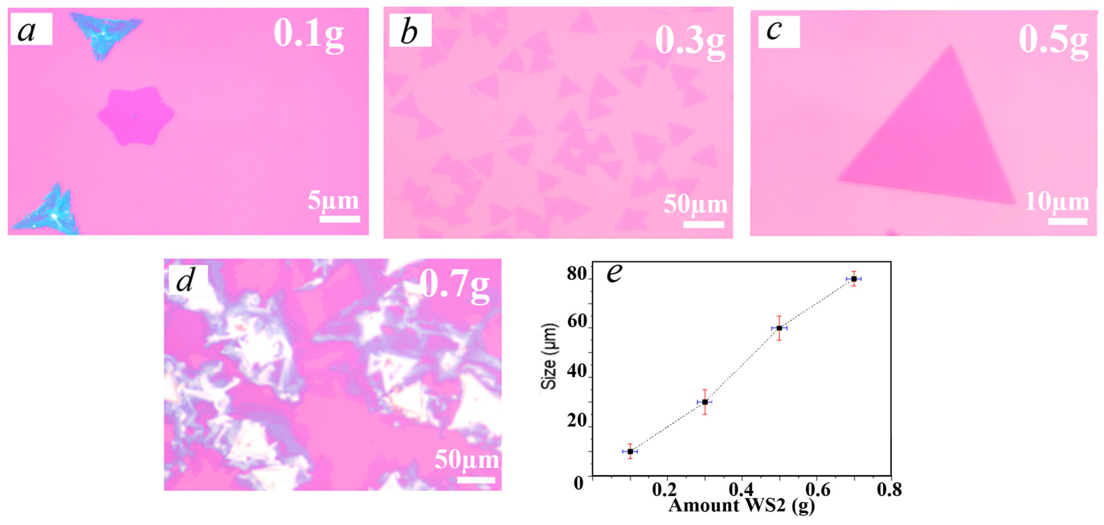
3.2. Quantity of Powder (Precursors)
The quantity of powder used throughout the growing process is likewise significant. While the growth dynamics of two-dimensional materials remain incompletely comprehended, it is widely acknowledged that two predominant growth modes are typically observed in the growth of 2D TMD material. (1) The Wx species experience adsorption and diffusion phenomena on the substrate surface, followed by a reaction with sulfur vapor atoms that leads to the formation of WS
2. (2) The groups of Wx react with sulfur atoms in the gaseous phase, leading to the formation of W
xS
y clusters that undergo adsorption, nucleation, and growth on the substrate. The potential for direct conflict between these two modes is contingent upon the concentration of powder present in the atmosphere. The present study involved loading varying quantities of WS
2 powder, specifically, 0.1, 0.3, 0.5, and 0.7 g, to examine the impact of WS
2 vapor concentration on the expansion of the WS
2 film. With a mere 0.1 g of WS
2 powder, the partial pressure of WS
2 vapor within the quartz tube was notably low, thereby facilitating the production of a flawed film. As illustrated in
Figure 3a, the sample contained a restricted quantity of triangular WS
2 flakes measuring approximately 10 µm. Additionally, numerous small spots with an irregular shape and an edge size of less than 5 µm were observed. The introduction of WS
2 powder in varying quantities between 0.3 to 0.5 g resulted in a notable increase in the quantity of triangular WS
2 domains on the substrate. Additionally, the average size of these domains increased from below 50 µm to over 100 µm (
Figure 3b,c).
As can be seen in
Figure 3d, when the WS
2 powder was further applied up to 0.7 g, the substrate was covered with more significant domains that had an edge length of less than 250 µm (unregulated growth in large sizes that are difficult to determine accurately) and a high number of microscopic particles. Most of these tiny particles were WxSy grains, which acted as seed nuclei and continuously interacted with S atoms to generate WS
2 flakes [
21]. Over time, the nearby flakes with the same crystallographic orientation expanded, and eventually, they fused to form an enormous domain.
Figure 3e shows that the enormous triangular field comprised many smaller triangular domains. This was quite simple to discern, as due to the high partial pressure of tungsten disulfide, the total number of crystal nuclei saw a substantial rise.
Figure 2f shows the relation between the mass of the source and the growing size. We note that the greater the mass, the greater the size due to many scattered precursors. We can consider that 0.5 g is the most appropriate mass due to the quality of growth and size. A rough edge was produced due to adjacent nuclei growing competitively while simultaneously experiencing a disordering of their crystal orientations [
22,
23]. In conclusion, the findings of the experiments described in this article indicate that loading an adequate quantity of powder is an essential factor in developing high-quality WS
2 films.
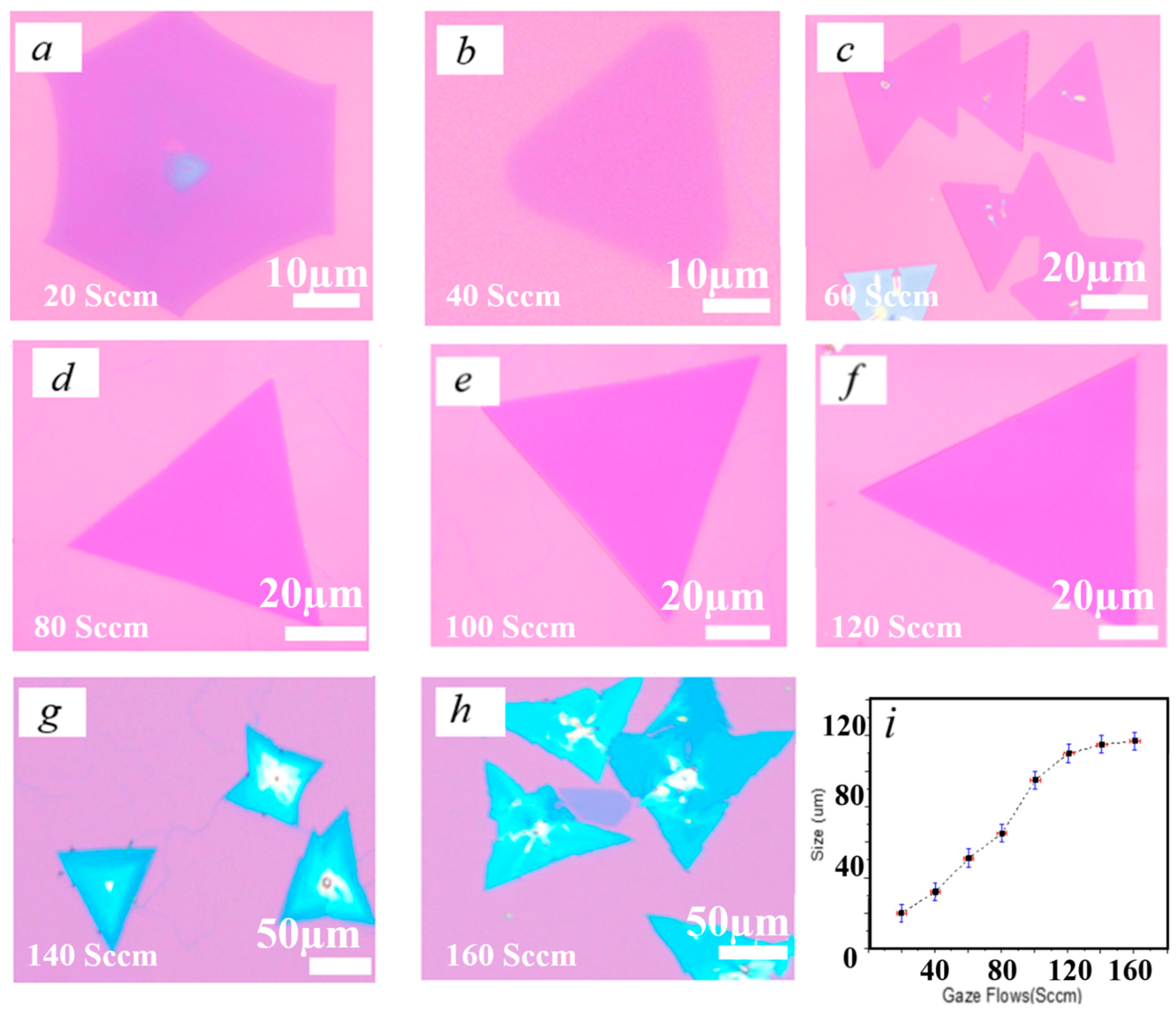
3.3. Gas Flows
To examine the impact of gas flow rate on film development, the gas flow rate was manipulated within a range of 20 to 160 Sccm, with increments of 20 Sccm. The aforementioned optimized parameters, namely the quantity of powder and temperature, were utilized to regulate additional growth conditions. An alteration in the size and morphology of WS
2 domains was observed upon an increase in the flow rate of N2 from 20 to 160 Sccm. The results depicted in
Figure 4 are deemed to be of utmost importance. The WS
2 film exhibited truncated triangular domains measuring 50 µm when subjected to gas flow rates ranging from 20 to 60 Sccm, as depicted in
Figure 4a–c. As depicted in
Figure 4d–f, an increase in flow rate from 60 to 100 Sccm reduced the length of the truncated side. Subsequently, the flakes underwent a metamorphosis into a triangular configuration characterized by sharp and smooth edges.
Simultaneously, there was a noticeable augmentation in the average domain magnitude, estimated to be approximately 60 µm. The domains ultimately undergo a cessation of morphological changes and continue to increase in size until they attain a diameter exceeding 100 µm while being subjected to a flow rate of 120 standard cubic centimeters per minute. Upon reaching a gas flow rate of 160 Sccm, it was concluded that there would be no additional increase in size. Based on current knowledge, it can be stated that WS
2 exists in a trigonal prismatic crystal structure in its bulk form, specifically in the 2H phase. During this particular phase, the coordination of each W atom occurs prism-likely with six S atoms in close proximity, creating a thermodynamically stable phase. It is posited that the initial stage of domain development involves the extension of a hexagonal nucleus comprising three sides of W zigzag (W-ZZ) terminations and an additional three sides of S zigzag (S-ZZ) terminations [
35]. The augmentation of gas volume traversing the quartz tube resulted in an elevated proportion of S vapor atoms being drawn towards the central area of the tube, thereby causing a reduction in the atomic concentration ratio of Mo to S. Warner et al. conducted a study on the influence of the molybdenum-to-sulfur atom ratio on the morphology of molybdenum disulfide (MoS2) films using crystal growth principles [
35]. Their findings showed that as the proportion of W:S atoms decreased to below 1:2, the growth rate of three W-zz terminations surpassed that of the other three S-zz terminations. The transformation process would lead to a metamorphosis of the domain shape, which would undergo a sequence of changes from a hexagonal form to a truncated triangular shape, ultimately culminating in an equilateral triangular configuration.
Moreover, the elevated flow rate facilitated the mass transfer phenomenon, increasing the crystal growth rate. The observed result was ascribed to the increased velocity of flow. As the gas flow rate was increased from 140 to 160 sccm, there was an observed increase in both the probability of defect formation and the level of anisotropy in growth. The observed phenomenon can be attributed to a regional thermal anomaly and an imbalance in precursor concentrations and pressure at a localized level. It could lead to instability. The atoms would not have had sufficient time to migrate to their appropriate lattice positions.
As a result, it can be observed from
Figure 4g,h that an increase in flow gas rate leads to a higher probability of roughness formation on the previously smooth edges of WS
2 films. There exists a direct relationship between flow and size. As illustrated in
Figure 4i, a direct relationship exists between the proportion of flow and the magnitude. It can be inferred from the findings that a correlation exists between temperature and flow, as demonstrated in the
Supplementary Documentation.
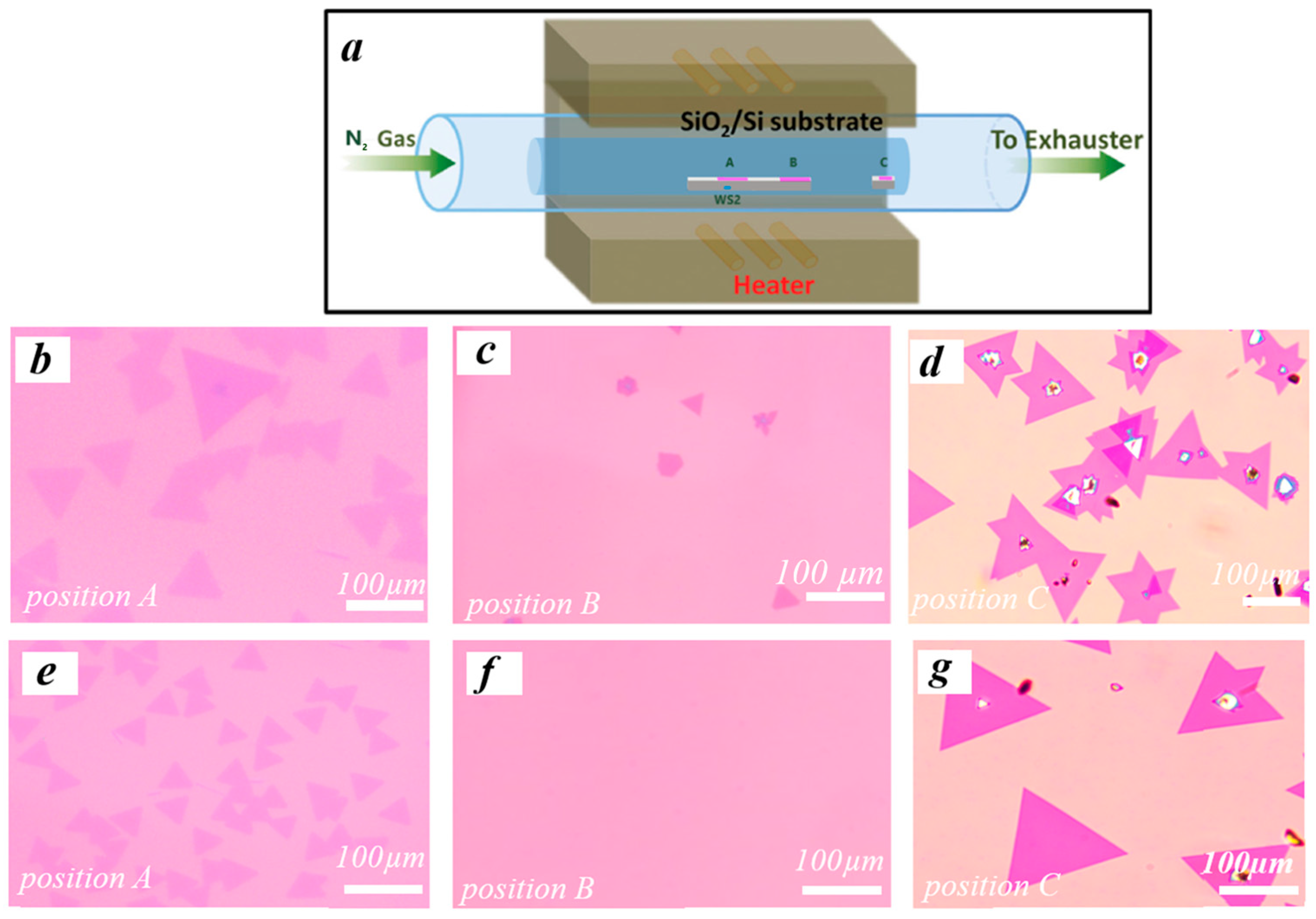
3.4. Substrate Position
The location of the substrate was another crucial factor. This section will examine and contrast the three different substrate locations. (This experiment was carried out according to the previously specified conditions. Slides A(b), B(c), and C(d) in one step (the three slides are placed together at the same time, condition and experiment) and an A(e), B(f), C(g) with separate experiments (the experiments in different periods, using one slide in each experiment, means that we conducted three experiments at this stage)), as shown in
Figure 5a. Substrate A was placed above the ceramic boat and faced down the tungsten disulfide powder, and substrate B was positioned downstream as substrate C was placed in the separating region so that the temperature was lower than the two substrates A and B (
AB = 6 cm/BC = 6 cm), shown in
Figure 5a.
The substrate’s placement was an essential element. This section aims to analyze and compare the three distinct locations of the substrate.
Figure 5a depicts the results of two experiments, one involving slides A and B and the other involving slide C. In accordance with the experimental setup depicted in
Figure 5a, substrate A was situated in an inverted orientation above the ceramic boat and directed towards the WS
2 powder. Substrate B was positioned downstream of substrate A, while substrate C was placed in the separating region, resulting in a temperature differential between A and B and C. Substrates A and B were measured to be 6 cm. The distance between substrates B and C was also 6 cm.
Elevated temperature conditions resulted in a heightened concentration of supersaturated precursor within the core of the tube, leading to a decreased density of crystallization nuclei. An increased level of thermal energy controlled the observed occurrence. Concurrently, due to the copious amount of precursors and a heightened atomic diffusion rate, it was determined that cultivating extensive single domains of WS
2 on substrates A and C was comparatively less challenging, as illustrated in
Figure 5b,d [
31]. The dimensions of these domains were measured to be 60–80 µm and 90–120 µm, respectively. Conversely, in the case of substrate B located downstream, the reduction in temperature resulted in a decrease in the level of supersaturation of the precursor, thereby facilitating the formation of additional nuclei on the substrate. This phenomenon occurred due to a decrease in temperature. The diminutive dimensions of the individual domains observed on substrate B (measuring less than 10 µm, as depicted in
Figure 5c) may be ascribed to the comparatively lower levels of precursor concentration and molecular kinetic energy in contrast to those present on substrate A, as previously noted [
31].
Concerning the substrate depicted in
Figure 5e–g, substrate A, the results were consistent with previously reported findings. Regarding substrate B, the findings were somewhat conventional, with less than 5 µm dimensions. It is plausible that substrate A in the prior trial altered the trajectory of the precursor towards substrate B, resulting in the development of diminutive dimensions. Regarding substrate C, the dimensions of growth were recorded to be 150 µm, which was observed to be the most significant among the three substrates. The phenomenon under consideration results from two key factors: temperature and the considerable spatial separation between the slice and origin. These factors collectively give rise to a substantial quantity of volatile precursors, subsequently affecting a marked augmentation in magnitude. Presented above is an opportunity to verify the accuracy of the information provided.
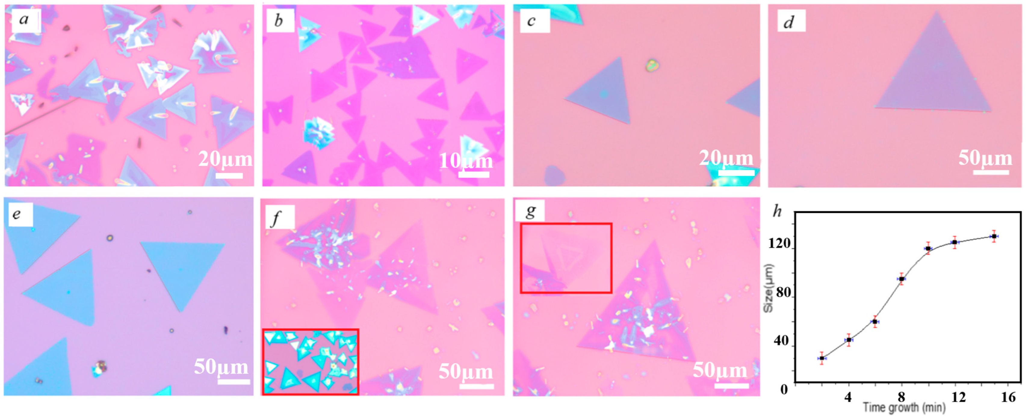
3.5. Growth Time
The growth time was adjusted between 2 and 15 min (in 2 min increments). The growth temperature was set to 1180 °C, Si/SiO
2 substrate on position C, flow 120 Sccm, and the amount of WS
2 powder was held constant at 0.5 g (
Figure 6).
As the duration of growth was prolonged, the domain size of the films exhibited a consistent increase, ranging from approximately 30 µm at 4 min to roughly 120 µm at 10 min. This trend is illustrated in
Figure 6a–e, where the domain sizes are denoted as FL ~40 µm at 5 min, BL ~60 µm at 6 min, ML ~95 µm at 8 min, and ML ~120 µm at 10 min. Nevertheless, the horizontal dimension did not grow further during the 12 and 15 min retention intervals. Various parameters, such as the substrate surface’s roughness, nucleation density, and the rate of molecular diffusion of gas, are postulated to be implicated. As per the principles of thermodynamics [
36], the alteration in free energy while undergoing growth can potentially determine or limit the extent of lateral growth. Furthermore, the complete triangular film would be susceptible to frequent collisions with adjacent gas molecules, potentially contaminating or compromising the original film’s integrity, leading to film defects. The findings depicted in
Figure 6f,g suggest that these imperfections can persist and damage the underlying substrate when exposed to elevated temperatures.
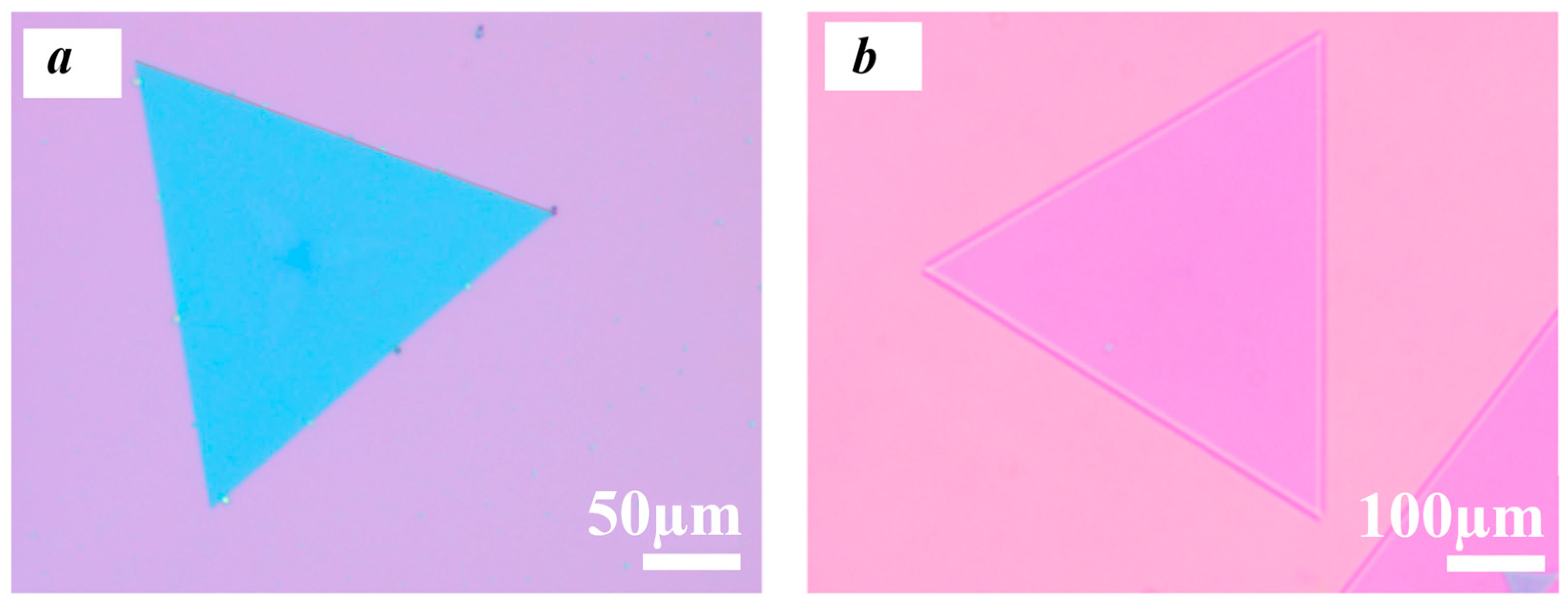
3.6. Direction
The issue at hand pertains to the inability of current synthesis techniques to attain accurate and manageable conveyance of solid-source vapor. The synthesis of materials may be subject to uncertainty due to the turbulent temperature disturbance of the evaporation source and the violent fluctuation of the substrate temperature during the heating process. The investigation of elevated temperatures for crystal growth and solid-source volatilization presents a difficulty owing to the accidental chemical vapor provision that arises before the preestablished growth temperature, which can lead to unregulated proliferation under circumstances where the source’s temperature is below 1100 °C. Crystals tend to develop at sluggish lateral growth rates, typically measuring less than 1 μm/s. A pre-annealing procedure was incorporated into the reverse flow, with a controlled duration preceding the transition of the flow to the forward direction. The aforementioned procedure was executed to attain more uniform nucleation and growth of two-dimensional crystals on the substrate, as illustrated in
Figure 1. During the temperature ramping and pre-annealing stage, the process entails the implementation of a reverse flow from the substrate to the source, while forward flow from the chemical vapor source is solely administered at the specific nucleation and growth temperature. The temperature protocol employed for the regulated expansion of WS
2 crystals during the heating stage is illustrated in
Figure 1 and
Figure S1. The supply of reactants is minimized. Upon reaching the designated growth temperature, which may be set at 1180 °C, the carrier gas flow is subsequently reversed to a forward direction. By circumventing the erratic results during the heating phase, it is possible to attain accurate steam distribution at a consistent temperature [
18]. The data presented in
Figure 7 illustrate a significant disparity between the two methodologies, wherein a growth of 300 μm was achieved in the standard scenario (unidirectional). The novel approach of utilizing two directions yielded a substantial quantity of high-quality material, measuring approximately 850 μm. The process involves implementing rapid or natural cooling techniques while extracting the substrate.
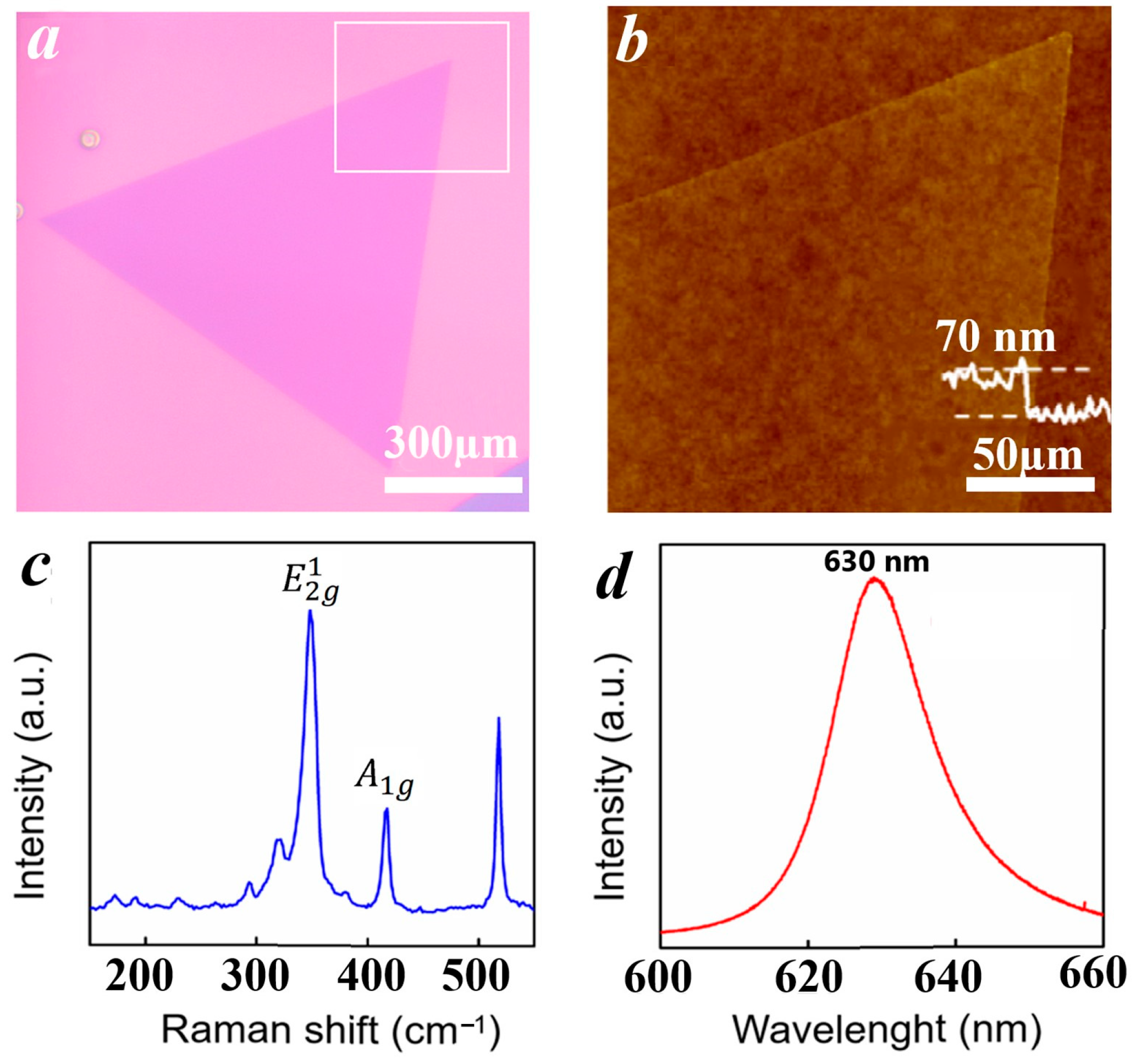
3.7. Characterization and Optimization
The present study analyzed the structural properties of several single crystals of tungsten sulfide to verify the quality of the sample (see
Figure 8a and
Figure S5). The AFM images revealed that the thickness of the single-crystal WS
2 sample was ~0.70 nm. Additionally, the surface of the single-crystal sample exhibited smoothness, which suggests that the prepared WS
2 was a monolayer crystal, as depicted in
Figure 8b. The application of Raman spectroscopy utilizing an excitation laser wavelength of 532 nm detected the existence of two significant peaks at 350.6 cm
−1 and 419.5 cm
−1. The peaks, as mentioned earlier, are indicative of the resonance modes of monolayer WS
2, specifically the
and
mode, as depicted in
Figure 8c [
37]. The photoluminescence spectrum of the specimen, as illustrated in
Figure 8d, demonstrates that the highest point is located at 630 nm. This discovery is consistent with the emission of a direct bandgap transition in monolayer WS
2. The findings indicate that the WS
2 sample that was prepared exhibits favorable crystalline properties. Future work will include a more comprehensive assessment of the caliber of sizable individual crystals acquired through the ultrarapid-growth technique.
4. Conclusions
This study underscores the importance of investigating the fundamental growth conditions to achieve good-quality materials. We have gained valuable insights into optimizing the synthesis process by systematically examining key factors such as temperature, the quantity of powder, flow gas, growth duration, gas flow direction, and substrate position, which is formed by adjusting each of the temperatures at 1180, the amount of the source at 0.5 g, the flow at 120 Sccm, the position of the slide at a distance of 8 cm, the growth time of 10 min, and the use of two directions, as previously indicated. Through meticulous control and manipulation of these growth parameters, we have successfully achieved a remarkable size of 850 µm, demonstrating the effectiveness of our approach. The ability to grow materials of such size highlights the significance of this research, as it opens new avenues for developing high-quality materials with tailored properties. The findings of this study serve as a valuable reference for researchers and pave the way for advancements in various fields, including electronics, energy storage, and catalysis, where materials of superior quality and size are vital for optimal performance.

 ,
, 


