Review

Fabrication of Ohmic Contact on N-Type SiC by Laser Annealed Process: A Review

1
Institute of Novel Semiconductors, Shandong University, Jinan 250100, China
2
Electronic Materials Research Group, School of Materials and Mineral Resources Engineering, University Sains Malaysia, Seberang Perai 14300, Pulau Pinang, Malaysia
*
Authors to whom correspondence should be addressed.
Crystals 2023, 13(7), 1106; https://doi.org/10.3390/cryst13071106
Submission received: 31 May 2023 / Revised: 26 June 2023 / Accepted: 14 July 2023 / Published: 16 July 2023
(This article belongs to the Special Issue Wide-Bandgap Semiconductors)

Abstract

:
In recent years, because of stringent needs in the fabrication of silicon carbide (SiC) power devices, laser annealing has been introduced to achieve local ohmic contact. In this paper, the laser annealing research for the ohmic contact process of SiC power devices is reviewed, which is mainly divided into four aspects: laser process mechanism, ohmic contact electrode materials, and substrate materials. The effect of laser parameters on ohmic contact and the annealing process on SiC diode devices is also reviewed. Progress of other substrate materials, namely 6H-SiC and semi-insulating 4H-SiC-based devices with laser annealed ohmic contacts, is also briefly discussed, in which formation of semi-insulating SiC ohmic contacts is derived from laser irradiation at the interface to produce 3C-SiC. Some experiment results have been shown in the passage, such as XRD, SEM, TEM, etc. In the review, it points out that the direction of application and development of the laser annealing process for improving the ohmic contact of SiC power devices is highly encouraging.

1. Introduction

Semiconductor power devices have been developing towards higher integration and higher power density. However, the performance of silicon (Si) power devices is approaching its limit. In recent years, the third generation of semiconductor materials such as silicon carbide (SiC) and other wide band gap semiconductors have gradually emerged, among which SiC has been developed rapidly because of its similar fabrication technology to Si-based devices. SiC has a higher breakdown field and electron saturation drift speed, wider band gap, and higher thermal conductivity, etc., than Si [1], which enables SiC to be used for high-power devices in harsh environment applications. In addition, the silicon carbide power device also has the advantages of small on-off loss and fast switching speed [1]. In view of the above characteristics, devices with two terminals, such as Schottky barrier diode (SBD), junction barrier Schottky diode (JBS), and PiN diode, have been fabricated on SiC as high-power devices. In addition, planar and trench Metal-Oxide-Semiconductor Field Effect Transistors (MOSFET) as three-terminal power devices on SiC were also reported [2]. SiC-based power devices, with their exceptional advantages, can be adopted in electric vehicles to reduce power consumption and photovoltaic to improve switching frequency, just to name a few.
Even though SiC reveals excellent device performances than Si-based devices, challenges in increasing material quality and size, increasing fabrication processes stability, yield, and reliability, as well as reducing substrate cost, are the essential topics of research. Ohmic contact, as one of the key building blocks in any SiC power device, affects the on-resistance and stability of the devices. Therefore, it is important to choose an appropriate ohmic contact process and electrode material for a dedicated type of device, depending on its application. The main requirements of an ohmic contact are a flat surface, low contact resistivity, and stability, which can be formed in two ways: (1) select the right metal to reduce the Schottky barrier height between metal and SiC, but it is challenging to find a suitable electrode material. The barrier height is affected by the work function of the electrode material and the quality of the interface between SiC and the electrode material. These two factors are influenced by processing technology. (2) Reduction in Schottky barrier width that can increase the probability of carrier tunneling through the barrier by increasing doping concentration in SiC [3]. Regardless of which strategies are adopted, the ohmic contact must undergo post-deposition annealing to achieve a low contact resistance. At present, the main annealing process of SiC power devices is by rapid thermal annealing with Ni [4]. The process was developed from the fabrication of silicon-based devices. This process technology is mature, with good uniformity and stability. However, devices that underwent rapid thermal annealing revealed a degradation in Schottky contact of a Schottky barrier diode (SBD) which reduced its reverse breakdown voltage [5] and reduction in channel mobility and increment in threshold voltage of a MOSFET. These are attributed to the process sequences in rapid thermal annealing, thermal budget for the annealing, and thermally affected regions. Typically, the subsequent rapid annealing process of an ohmic contact requires high temperature and is performed after the formation of front Schottky contact in making an SBD. Similarly, annealing of the backside ohmic contact is formed after the formation of front side processes of a MOSFET. In view of the above issues, a new strategy is needed to reduce the ohmic contact resistance via annealing in shortest period of time and yet the thermal budget absorbed by the material is localized. Therefore, laser processing technology has been proposed to address these challenges.
Laser has been applied to many applications in different industries. In the semiconductor industry, lasers have been used for dicing and lift-off processes (laser cutting), marking, etc. For the annealing process, a pulsed laser was used [6,7] and showed encouraging results with the laser energy in local contact with the surface irradiated area and not affecting other regions in the device [8]. Hence, this is the main objective of this review to compile and analyze the latest development of laser annealing adopted in producing a high-quality ohmic contact in SiC power devices. The process and influencing factors of laser annealing have been studied by theoretical calculations and simulation modeling [9,10,11], while some researchers have experimentally verified the feasibility of laser annealing. In addition, laser annealing can also be applied to activation and lattice repair after ion implantation [12].

2. Research Direction and Progress

At present, the research of laser thermal annealing can be divided into the following parts: laser process mechanism, ohmic contact electrode materials, substrate materials, device preparation, etc. For laser annealing, different process parameters have been investigated but mainly on wavelength and energy [8]. For an electrode material to form an Ohmic contact, it is closely related to the substrate material. A vast majority of the works reported were based on n-type 4H-SiC, as opposed to other substrates, such as 6H-SiC, semi-insulating 4H-SiC [13], and only Ni and Ti-based electrode materials have been reported [7,14,15]. Although different types of power device architectures can be fabricated to investigate the effect of laser annealing on the performance of ohmic contact, only simple device structures were used such as Schottky barrier diode and junction barrier Schottky diode [16,17].

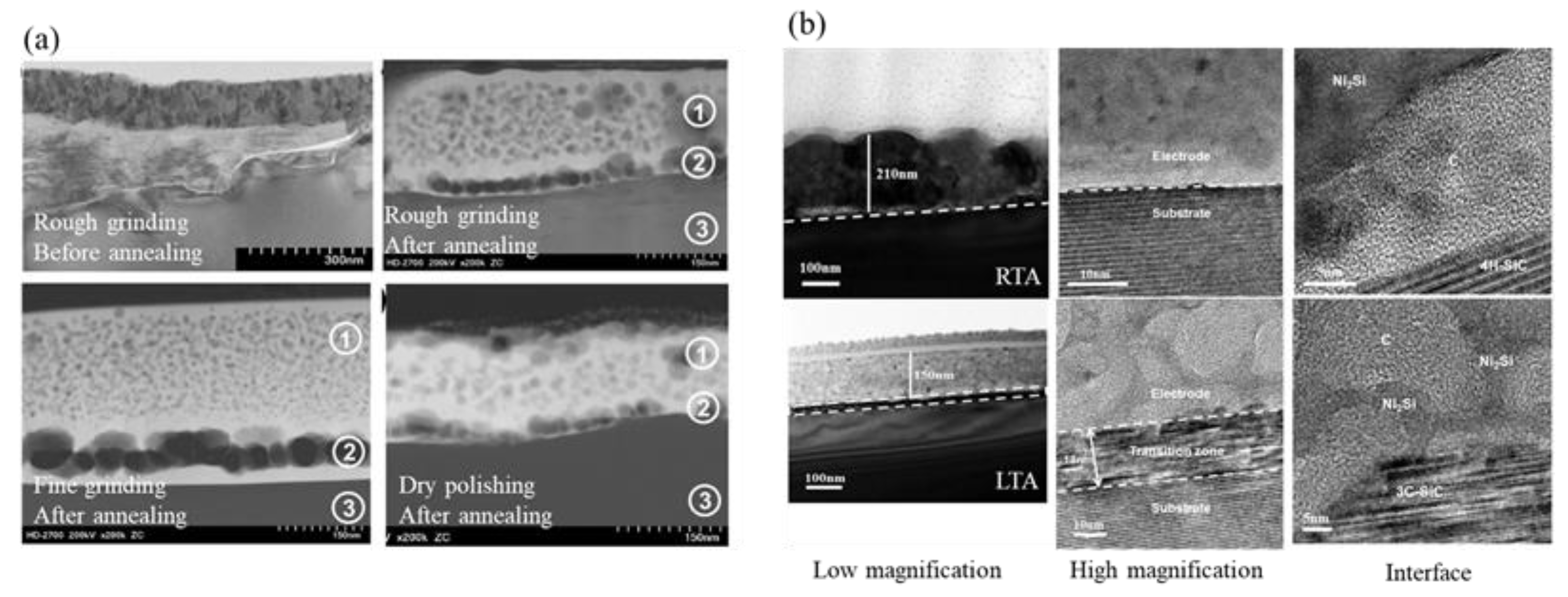
2.1. Laser Process Mechanism

Laser processing parameters are directly affecting the contact resistivity of the metal/SiC system during laser annealing. The commonly used laser annealing process device and principle are shown in Figure 1a, which is generally composed of a laser, a scanner, and a closed chamber. First, the sample is loaded into a chamber, and the laser spot size is adjusted by controlling the height of the sample stage. Then, the air in the chamber is evacuated before flowing into an inert type of working gas, such as nitrogen and argon, to prevent oxidation of the sample during processing. In the coupling of the laser and scanner, the energy density of the laser is controlled by adjusting the laser power, with the spot overlap rate controlled by the scanning rate of the scanner. This resulted in a uniform annealed area on the sample, as shown in Figure 1a.
At present, there are many types of lasers used in laser annealing, which can be mainly divided into two categories: Gaussian beam and flat-top beam. Huerner [18] used a Gaussian laser beam with a wavelength of 1070 nm to anneal 100 nm thick Ni on a C-face 4H-SiC substrate. Additionally, through the optimization of power and processing time, it successfully achieved a low contact resistance of 6.5 Ω, which is lower than the 10.3 Ω of the rapid thermal annealed sample. However, the problem with a Gaussian beam is that its energy is unevenly distributed with space. If the beam size is too small at the same energy, the obtained surface morphology will be poor because of the transient high temperature. However, the spot size used in the experiment is 7.1 mm, which is too large and reduces the advantages of laser annealing in localization and selectivity. In order to solve this problem, researchers began to use flat-top beams. Berger [19] used a 355 nm flat-top laser to anneal 100 nm thickness Ti on 4H-SiC. The effects of different energy densities and different overlap rates were systematically explored by changing the laser parameters. It is found that overlapping conditions have a great influence on contact morphology. The topography of ohmic contacts generated by high overlap was poor. Therefore, the contact surface can be greatly improved by reducing the overlap rate and maintaining ohmic characteristics by changing the energy density at the same time (Figure 1d) [19]. As shown in Figure 1b,c, with the increase in energy density, the metal-semiconductor contact changed from rectifying characteristics to ohmic contact characteristics, and the lowest contact resistivity of 1.4 × 10⁻⁴ Ω·cm2 was obtained at an energy density of 4.25 J/cm2. The contact resistivity of this literature is three times lower than that of a laserannealed Ti contact, but the energy density is almost twice as high.
As shown in Table 1, a direct comparison of the ohmic contact performance of the widely used electrode materials, namely Ni and Ti, on SiC after laser annealing is difficult. This is because a huge variation of wavelength, pulse width, frequency, and other parameters of the lasers had been used, and the outcomes were also in huge variation. In general, strong absorption of Ti and Ni happens at a wavelength below 370 nm with a wavelength of 355 nm and is commonly used in flat-top lasers. Short wavelength lasers are mainly absorbed by the metal electrodes, thus heating up the reaction with SiC. Longer wavelengths, such as 1064 nm, are absorbed less by the metal and therefore absorbed by the SiC, resulting in a temperature rise of the SiC that affects the structure of the front side. Therefore, the shorter wavelength 355 nm laser is more advantageous for laser annealing. On this basis, the ohmic contact energy density range is generally 2–4 J/cm2. Theoretically, the pulse width and repetition frequency of the laser are related to the temperature change of the sample in a short period of time, which has an impact on the morphology and reaction of the sample. However, there is currently no work being reported on the effects of pulse width and frequency on ohmic contact characteristics. However, the effects of various laser wavelengths, pulse width, and other parameters need to be systematically studied experimentally. In addition, the effect of the annealing atmosphere on reaction products and contact resistance is also worth studying. The stability of laser annealing devices and the mass production of commercial applications still need to be developed.

2.2. Electrode Materials for Ohmic Contact

The N-type SiC laser annealing process is developed from the traditional rapid annealing process. The commonly used ohmic contact metals are Ni and Ti. Among these, Ni can react with Si in silicon carbide at high temperatures to form a nickel-silicon complex, which is considered the basis for the formation of ohmic contact. However, because the C element in SiC does not participate in the reaction, C clusters are formed and lead to the precipitation of C, which affects the subsequent metal adhesion. Therefore, it is necessary to optimize the results of the laser annealing process from two aspects as follows: contact resistivity and carbon distribution [20]. The advantage of using Ti as the electrode material is due to its chemical reaction with both Si and C of SiC individually to form other phases that can prevent C precipitation and improve surface morphology after annealing [21]. However, the contact resistivity of Ti/SiC is difficult to meet the needs of the power device at present. Therefore, finding suitable metals or optimizing ohmic contact by alloying various metals has always been one of the research hotspots.
At present, many studies on laser-annealed Ni-based ohmic contact on SiC [5,6,20,22,23]. A series of studies have been conducted by correlating electrical properties with surface morphology and reacted products after annealing by using IV measurement, X-ray diffraction (XRD), cross-sectional and surface scanning electron microscopy (SEM), and TEM. Part of the experimental results are shown in Figure 2 [6,20,23]. In Figure 2a, XRD characterization has been carried out in most of the literature. However, it may contain phases of NiSi, Ni2Si, etc., after being annealed with a fluence of 3.8 J/cm2. These compounds formed between SiC and Ni according to XRD results shown in Figure 2a depending on the temperature of reaction and thickness of Ni. The formation of Ni2Si is considered the main phase that contributes to the low resistance of the ohmic contact. In addition, SEM and TEM results in Figure 2c,d also confirmed the existence of complex grains at the interface and showed that the excess of C in SiC aggregates into clusters or precipitates located on the surface of Ni. Zhou also observed similar structures with comparable chemical composition and phases after annealing the same material system by laser. The literature suggests that the phase contributed to the low contact resistivity after laser annealing [20]. Kawakami explored the influence of different laser energy densities on the reaction between SiC and Ni. As shown in Figure 2b, with the increase in laser energy density, the temperature in the irradiation region increases; hence, the contact characteristics change from rectifying to ohmic behavior [23]. In another research, by optimizing process parameters such as energy and number of pulses, a contact resistance as low as 4.8 × 10⁻⁵ Ω·cm2 was achieved, which is comparable to the result of the traditional rapid annealing process [5].
The main reason for using Ti as an ohmic contact electrode is the reaction of Ti with both Si and C in SiC to form Ti5Si3 and TiC independently (Figure 3a) [19,21]. With this, it can prevent precipitation of C on the surface of electrode material during the annealing process, thus improving the adhesion of the metal when it is getting thicker [24]. The laser annealing experiments of Ti/SiC were carried out by Silva and Badalàa with contact resistivity of 7.9 × 10⁻⁵ Ω·cm2 and 1.0 × 10⁻⁴ Ω·cm2, respectively, were obtained [21,24]. The XRD results in Figure 3a show that the reaction between Ti and SiC produces Ti5Si3 and TiC grains. In addition, for higher energy density, a complete reaction with good crystallization has been recorded. However, based on TEM results (Figure 3b), it is difficult to distinguish between Ti5Si3 and TiC grains. Only the presence of C in Ti-Si-C at the interface can be seen. De Silva also compared the contact resistance of the same process condition, and the physical thickness of Ti and Ni deposited individually on SiC with the Ti electrode recorded a lower contact resistance (Figure 3c). This may attribute to different laser absorption rates and reaction temperatures of those two metals [21,25].
In addition to the single metal as electrode material, some studies have also begun to focus on optimizing C distribution and controlling C precipitation to prepare for subsequent metal deposition aiming to lower the contact resistivity. On this basis, other metals, such as Nb and Mo, or alloy layers which are combined with Ni are explored [26,27]. It can be seen from the XRD and TEM results in Figure 4a,b that Nb can react with rich carbon elements, which changes the carbon distribution at the interface between the metal layer and SiC. However, from the comparison of the contact resistivity under different laser energies, the optimization of the double-layer metal structure is not obvious. As shown in Figure 4c, electrodes containing only Nd and Ni have a higher ohmic contact resistance. The laser annealing effect of the alloy is better, and the contact resistivity of the NbNi/SiC structure can reach the lowest 5.3 × 10⁻⁴ Ω·cm2 when the energy density is 2.25 J/cm2. This result is higher than that of pure Ni electrode contact resistivity under the same conditions reported in other studies [5]. This may be due to unoptimized laser conditions. The idea of using alloys as electrodes undoubtedly provides another idea for laser annealing of ohmic contact.
Although many studies have tried to explore the formation mechanism of ohmic contact in the laser annealing process through different characterization techniques, namely crystallization by XRD, interfacial morphology and structure by SEM and TEM, as well as chemical distribution by XPS. There is no unified answer to the principle, especially under different types of metal and experimental conditions. At present, the mainstream view is that: (1) The chemical composite formed by metal and SiC is the key to the formation of ohmic contact, (2) the metal and SiC reaction with C aggregated at the interface is a kind of efficient conductor, and (3) as carbon moves to the surface of SiC, there may be a large number of carbon vacancies inside SiC as positively charged donors, which reduces the height and width of Schottky barrier. The current electrode material system has little scope for selection. New electrode materials need to be found in order to obtain better ohmic contact in terms of absorption rate to the laser and response mechanism to the SiC.

2.3. SiC Substrate Materials

Common polytypes of SiC crystal mainly include 3C-SiC, 4H-SiC, and 6H-SiC. The ohmic contact of electrode materials and processes depends on different types and concentrations of dopant and crystal faces. Mostly, research has been concentrated on n-type, C-faces 4H-SiC (000-1) due to the requirement of forming a back ohmic contact of diode or transistor. However, due to the unique advantages of laser annealing, some works [28,29] were conducted in other crystallographic directions, and planes have gradually developed. Mazzamuto [28] compared different substrate thinning strategies before metal deposition and laser annealing of 4H-SiC and proved that the top nickel silicide formed during the laser annealing. As shown in Figure 5a, the carbon nanoclusters formed at the NiSi/SiC interface, in addition to the defects caused by thinning, are repaired near the SiC substrate. The repair of lattice defects by laser annealing is one of the research hot topics. Eryu [29] used laser-treated 6H-SiC as a substrate before Ni was thermally evaporated so that the gas phase of Ni reacted with SiC to achieve an ohmic contact. It demonstrated that surface damage of SiC can be removed during the laser annealing process. Cheng [13] compared the contact resistivity of rapid thermal and laser-annealed Ni with 150 nm thick deposited on a silicon surface semi-insulating SiC substrate with the latter annealed strategy revealed a lower resistivity (1.97 × 10⁻³ Ω·cm2). Based on TEM (Figure 5b), it was found that in addition to Ni-Si phase and C clusters, 3C-SiC was also formed at the interface after laser treatment, but this was not detected in the rapid thermal annealed sample. These studies prove the universality of laser annealing for different SiC substrates. However, the current researches are insufficient as most of the works were focused on N-type, C-face, and 4H-SiC. It is still lacking research in N-type, both P-types, 4H-SiC, and other crystalline phases of SiC substrates. In particular, the source ohmic contact of SiC power devices is usually a simultaneous P-type and N-type reaction, which is also an important part of the development prospects of laser annealing.

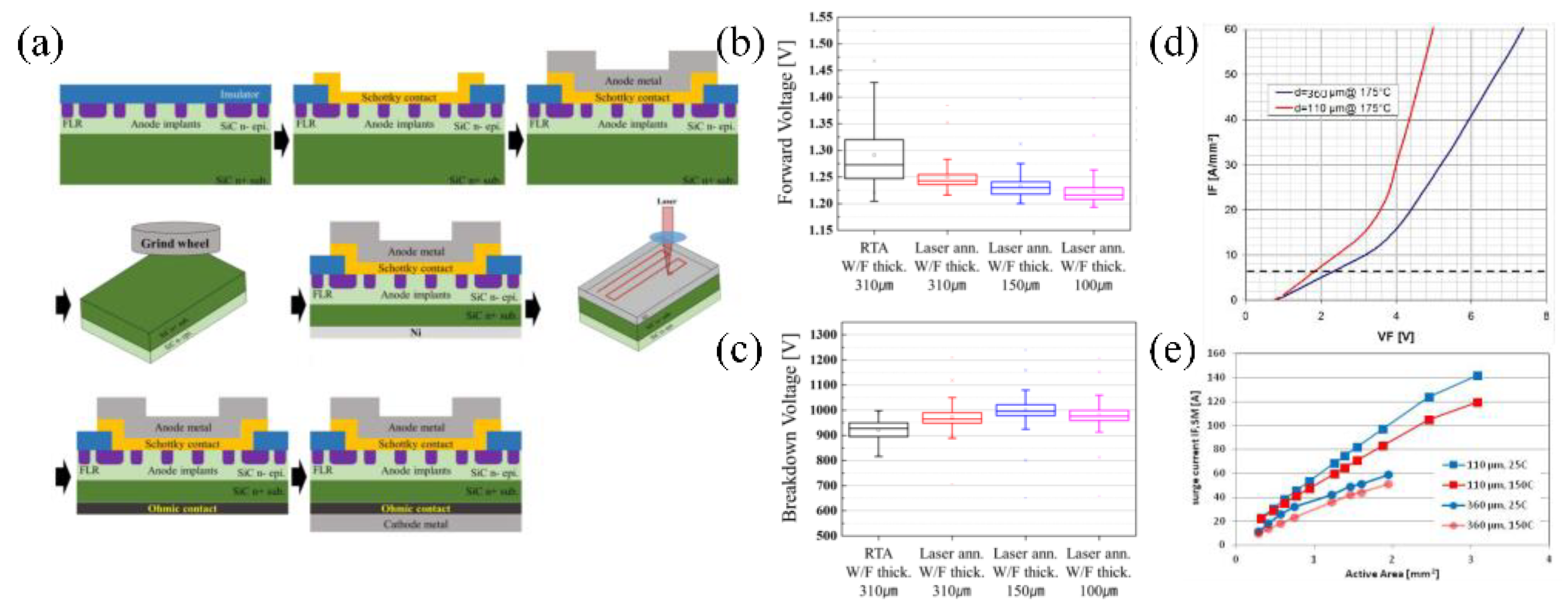
2.4. Device Preparation and Application

The main intention of laser annealing on ohmic contact at the backside of SiC power devices is to reduce the contact resistance and yet not to induce any impact on the completed structure fabricated on the front side. Mostly diodes were used as the test structures due to their simplicity for the investigation of laser annealing. So the effects of laser annealing on the conduction and reverse cut-off characteristics of the diodes can be established. Since the laser annealing process effect is localized at the backside ohmic contact, the maximum thermal conduction through the substrate cannot be reached up to 100 μm [17]. Hence, the frontside fabricated structure is not affected during the annealing process.
The traditional diode preparation process requires epitaxial preparation of the drift layer at about 1600 °C. Followed by ion implantation (such as edge termination, merged PN-Schottky structure) and annealing to activate the injection ions at about 1700 °C. After which, it is necessary to deposit the back metal and perform a rapid annealing process at about 1000 °C. Then, a metal is deposited on the front side to prepare a Schottky junction. The thickened metal on the back side is deposited for subsequent welding and then passivation and repair of edge termination. This process sequence was performed to prevent the effect of the frontside Schottky structure during rapid annealing, but the on-resistance was too large due to process limitations that prevented thinning the substrate. The proposed laser annealing process is able to solve this problem, and the specific process step is shown in Figure 6a. After ion implantation and activation, the frontside Schottky structure is prepared. The passivation treatment and repair of edge termination, as well as other frontside processes, are carried out. Additionally, then thinning from the C surface of silicon carbide is carried out. Followed by ohmic contact back metal deposition and laser annealing. Finally, thickening of the back side metal is performed. The procedure is shown in Figure 6a. Due to the local heating characteristics of laser annealing, the heat is dissipated within a short range, so it does not affect the Schottky structure that has been prepared on the front side [30].
Researchers have demonstrated the feasibility of laser annealing. Kim [17] compared laser and rapid thermal annealing of JBS with different thicknesses. As shown in Figure 6b,c, the forward opening voltage of laser-annealed samples is generally lower than that of rapid-annealed samples; with the decrease in thickness, the opening voltage is reduced. The on-voltage of the 100-μm-thick laser annealing sample is 1.33 V at 20 A, and the on-resistance is reduced by 22% if compared with the rapid annealing process. Moreover, the reverse breakdown voltage is generally higher than that of the rapid thermal annealing process.
In addition, laser annealing on SiC power devices with thin substrates can reduce on-resistance and switching loss. Rupp [30] deposited a NiSi layer on a thinned SiC substrate and formed an ohmic contact below 1 × 10⁻⁵ Ω·cm2 when treated with a 310 nm laser. Its forward opening IV and surge results are shown in Figure 6d,e with increasing current density and reducing the switching loss. After mechanical polishing of the SiC substrate, a Ni/4H-SiC structure was annealed using a 355 nm laser to produce a 1200 V/15 A SiC JBS diode with a thickness of 100 μm [8]. The results show that when the laser energy density is 1.8 J/cm2, a good ohmic contact resistivity of 7.42 × 10⁻⁵ Ω·cm2 can be obtained. It was proved that the thinning and laser annealing treatment did not reduce the performance of the reverse breakdown voltage, but the forward opening voltage was reduced by 0.15 V, and the current density was increased by 41.27% if compared with the unthinned sample.
Rusch [16] fabricated a 6/650 V SiC diode by thinning of substrate and laser annealing of backside metal ohmic contact. The turn-on voltage (VF) of the device dropped from 1.78 V in the rapid annealing process to 1.62 V at a rated current of 6 A, and the leakage current of the device is less than 1 μA at a rated voltage of 650 V. It was also maintaining a blocking capability of more than 1.1 kV. In addition, Badala [31] prepared SBD with a similar structure and method, which proved the advantages in reducing the on-voltage. Rascuna [32] also applies a laser annealing process in the preparation of SiC power diodes. The work proved that the laser annealing process can reduce the on-voltage and on-resistance of the SiC power devices. In general, only limited device structures (SBD and JBS) have been investigated. Therefore, it is important to study the effect of laser annealing on other types of power devices, such as metal semiconductor field effect transistors, insulated-gate bipolar transistors, etc.
As the technology matures, laser annealing will be applied to the preparation of the frontal source electrode, and it will be interesting to see how the performance of SiC MOSFETs, IGBTs, and other devices will change.

3. Summary and Outlook

Through the above discussion, current research on laser annealing of ohmic contact was mainly focused on the preparation of Ni and Ti-based metal on N-type, C-face, and 4H-SiC power diodes. Based on the literature, a relatively good contact resistivity has been obtained, and a significant reduction in on-resistance and on-voltage of diodes. However, the research of electrode materials needs to be developed and broadened, and there is less research on P-type SiC and other polytypes of SiC. Further, the optimization of laser and process parameters was mainly focused on energy density and scanning overlap rate. Further exploration of laser wavelength, pulse width, frequency, etc., is needed to understand the effects of laser on the formation of chemical composition and phases on the improvement in contact resistance. As for the application, in addition to diodes, there are mature MOSFET and IGBT structures under development for power applications, where it is unknown how laser annealing on the performance of these types of power devices. We believe that in the near future, laser annealing can be widely used in the process of industrial preparation of SiC power devices.

Author Contributions

Conceptualization, G.L. and D.Z.; methodology, M.X. and Y.C.; validation, G.L., M.X. and J.H.; investigation, G.L., Y.Z., H.N. and S.L.; resources, M.X., B.Z. and J.H.; writing—original draft preparation, G.L.; writing—review and editing, M.X., K.Y.C., J.X. and H.L.; visualization and editing, G.L., Y.C. and P.C.; supervision, J.H. and X.X.; project administration, M.X. and J.H.; funding acquisition, J.H. and X.X. All authors have read and agreed to the published version of the manuscript.

Funding

This research was funded by the Major Science and Technology Innovation Project of Shandong Province (2022CXGC010103), the Natural Science Foundation of Shandong Province (202102220483 and 2022HWYQ-019), and the National Natural Science Foundation of China (62204142).

Data Availability Statement

Not applicable.

Conflicts of Interest

The authors declare no conflict of interest.

References

  1. Millán, J.; Godignon, P.; Perpiñà, X.; Perez-Tomás, A.; Rebollo, J. A Survey of Wide Bandgap Power Semiconductor Devices. IEEE Trans. Power Electron. 2014, 29, 2155–2163. [Google Scholar] [CrossRef]
  2. She, X.; Huang, A.Q.; Lucia, O.; Ozpineci, B. Review of Silicon Carbide Power Devices and Their Applications. IEEE Trans. Ind. Electron. 2017, 64, 8193–8205. [Google Scholar] [CrossRef]
  3. Zhe, C.F. Silicon Carbide: Materials, Processing & Devices; CRC Press: Boca Raton, FL, USA, 2003; Volume 20. [Google Scholar]
  4. Han, S.Y.; Shin, J.-Y.; Lee, B.-T.; Lee, J.-L. Microstructural interpretation of Ni ohmic contact on n-type 4H–SiC. J. Vacuum Sci. Technol. B Microelectron Nanometer Struct. Process. Meas. Phenom. 2002, 20, 1496–1500. [Google Scholar] [CrossRef] [Green Version]
  5. Liu, M.; He, Z.; Niu, Y.; Wang, X.; Yang, F.; Yang, F. Ni/4H-SiC Ohmic Contact Formed by Laser Annealing. Semicond. Technol. 2016, 41, 690–694. [Google Scholar]
  6. Adelmann, B.; Hurner, A.; Schlegel, T.; Bauer, A.J.; Frey, L.; Hellmann, R. Laser Alloying Nickel on 4H-Silicon Carbide Substrate to Generate Ohmic Contacts. J. Laser Micro Nanoeng. 2013, 8, 97–101. [Google Scholar] [CrossRef] [Green Version]
  7. Vlasov, I.I.; Lyalin, A.A.; Obraztsova, E.D.; Simakin, A.V.; Shafeev, G.A. Formation of ohmic contacts with SiC by laser ablation. Quantum Electron. 1998, 28, 673–676. [Google Scholar] [CrossRef]
  8. Qijun, L. Substrate Thinning and Laser Annealing Process of SiC JBS Diodes. Semicond. Fabr. Technol. 2021, 46, 12. [Google Scholar]
  9. Ding, J.; Li, X.; Yang, K.; Zhu, Y. Numerical simulation on controlling the front-side temperature of thinned SiC substrate during ohmic contact to Ni or Ti using back-side laser annealing. J. Appl. Phys. 2022, 132, 035703. [Google Scholar] [CrossRef]
  10. Gueorguiev, G.; Stafström, S.; Hultman, L. Nano-wire formation by self-assembly of silicon–metal cage-like molecules. Chem. Phys. Lett. 2008, 458, 170–174. [Google Scholar] [CrossRef]
  11. Kakanakova-Georgieva, A.; Ivanov, I.G.; Suwannaharn, N.; Hsu, C.-W.; Cora, I.; Pécz, B.; Giannazzo, F.; Sangiovanni, D.G.; Gueorguiev, G.K. MOCVD of AlN on epitaxial graphene at extreme temperatures. Crystengcomm 2021, 23, 385–390. [Google Scholar] [CrossRef]
  12. Calabretta, C.; Agati, M.; Zimbone, M.; Boninelli, S.; Castiello, A.; Pecora, A.; Fortunato, G.; Calcagno, L.; Torrisi, L.; La Via, F. Laser Annealing of P and Al Implanted 4H-SiC Epitaxial Layers. Materials 2019, 12, 3362. [Google Scholar] [CrossRef] [Green Version]
  13. Cheng, Y.; Lu, W.Y.; Wang, T.; Chen, Z.Z. Fabrication of Ohmic contact on semi-insulating 4H-SiC substrate by laser thermal annealing. J. Appl. Phys 2016, 119, 225705. [Google Scholar] [CrossRef]
  14. Hellinger, C.; Rusch, O.; Rommel, M.; Bauer, A.J.; Erlbacher, T. Low-resistance ohmic contact formation by laser annealing of N-implanted 4H-SiC. Mater. Sci. Forum 2020, 1004, 718–724. [Google Scholar] [CrossRef]
  15. Zhou, Z.W.; Zhang, Z.Z.; He, W.W.; Hao, J.Y.; Sun, J.; Zhang, F.; Zheng, Z.D. The Ohmic Contact of 4H-SiC Power Devices by Pulse Laser Annealing and Rapid Thermal Annealing. Mater. Sci. Forum 2020, 1004, 712–717. [Google Scholar] [CrossRef]
  16. Rusch, O.; Hellinger, C.; Moult, J.; Corcoran, Y.; Erlbacher, T. Reducing On-Resistance for SiC Diodes by Thin Wafer and Laser Anneal Technology. Mater. Sci. Forum 2020, 1004, 155–160. [Google Scholar] [CrossRef]
  17. Kim, K.; Kang, Y.; Yun, S.; Yang, C.; Jung, E.; Hong, J.; Kim, K. Reduced On-Resistance and Improved 4H-SiC Junction Barrier Schottky Diodes Performance by Laser Annealing on C-Face Ohmic Regions in Thin Structures. Coatings 2022, 12, 777. [Google Scholar] [CrossRef]
  18. Huerner, A.; Schlegl, T.; Adelmann, B.; Mitlehner, H.; Hellmann, R.; Bauer, A.J.; Frey, L. Alloying of Ohmic Contacts to n-type 4H-SiC via Laser Irradiation. Mater. Sci. Forum 2013, 740, 773–776. [Google Scholar] [CrossRef]
  19. Berger, C.; Alquier, D.; Michaud, J.F. Optimisation of Ti Ohmic Contacts Formed by Laser Annealing on 4H-SiC. Mater. Sci. Forum 2022, 1062, 219–223. [Google Scholar] [CrossRef]
  20. Zhou, Z.W.; He, W.W.; Zhang, Z.Z.; Sun, J.; Schoner, A.; Zheng, Z.D. Characteristics of Ni-based ohmic contacts on n-type 4H-SiC using different annealing methods. Nanotechnol. Precis. Eng.-Nami Jishu Yu Jingmi Gongcheng 2021, 4, 013006. [Google Scholar] [CrossRef]
  21. De Silva, M.; Kawasaki, T.; Miyazaki, T.; Koganezawa, T.; Yasuno, S.; Kuroki, S.I. Formation of epitaxial Ti-Si-C Ohmic contact on 4H-SiC C face using pulsed-laser annealing. Appl. Phys. Lett. 2017, 110, 252108. [Google Scholar] [CrossRef]
  22. Badalà, P.; Rascunà, S.; Cafra, B.; Bassi, A.; Smecca, E.; Zimbone, M.; Bongiorno, C.; Calabretta, C.; La Via, F.; Roccaforte, F.; et al. Ni/4H-SiC interaction and silicide formation under excimer laser annealing for ohmic contact. Materialia 2020, 9, 100528. [Google Scholar] [CrossRef]
  23. Kawakami, H.; Naoi, Y.; Tomita, T. Femtosecond laser–assisted thermal annealing of Ni electrode on SiC substrate. AIP Adv. 2018, 8, 065204. [Google Scholar] [CrossRef] [Green Version]
  24. Berger, C.; Alquier, D.; Bah, M.; Michaud, J.F. Electrical, morphological and structural properties of Ti ohmic contacts formed on n-type 4H-SiC by laser thermal annealing. Mater. Sci. Semicond. Process. 2022, 151, 106983. [Google Scholar] [CrossRef]
  25. de Silva, M.; Kawasaki, T.; Kuroki, S. Low Resistance Ti5Si3/TiC Ohmic contact on Ion-Implanted n-Type 4H-SiC C Face. Mater. Sci. Forum 2018, 924, 409–412. [Google Scholar] [CrossRef]
  26. de Silva, M.; Ishikawa, S.; Kikkawa, T.; Kuroki, S.I. Low Resistance Ohmic Contact Formation on 4H-SiC C-Face with NbNi Silicidation Using Nanosecond Laser Annealing. Mater. Sci. Forum 2016, 858, 549–552. [Google Scholar] [CrossRef]
  27. De Silva, M.; Ishikawa, S.; Miyazaki, T.; Kikkawa, T.; Kuroki, S.I. Formation of amorphous alloys on 4H-SiC with NbNi film using pulsed-laser annealing. Appl. Phys. Lett. 2016, 109, 012101. [Google Scholar] [CrossRef]
  28. Mazzamuto, F.; Halty, S.; Tanimura, H.; Mori, Y. Low Thermal Budget Ohmic Contact Formation by Laser Anneal. Mater. Sci. Forum 2016, 858, 565–568. [Google Scholar] [CrossRef]
  29. Eryu, O.; Kume, T.; Nakashima, K.; Nakata, T.; Inoue, M. Formation of an ohmic electrode in SiC using a pulsed laser irradiation method. Nuclear Instrum. Methods Phys. Res. Sect. B-Beam Interact. Mater. At. 1997, 121, 419–421. [Google Scholar] [CrossRef]
  30. Rupp, R.; Kern, R.; Gerlach, R. Laser backside contact annealing of SiC power devices: A prerequisite for SiC thin wafer technology. In Proceedings of the 2013 25th International Symposium on Power Semiconductor Devices & IC’s (ISPSD), Kanazawa, Japan, 26–30 May 2013; pp. 51–54. [Google Scholar]
  31. Badalà, P.; Smecca, E.; Rascunà, S.; Bongiorno, C.; Carria, E.; Bassi, A.; Bellocchi, G.; Castorina, S.; Tringali, C.; La Magna, A.; et al. Structural and Electrical Characterization of Ni-Based Ohmic Contacts on 4H-SiC Formed by Solid-State Laser Annealing. Mater. Sci. Forum 2022, 1062, 417–421. [Google Scholar] [CrossRef]
  32. Rascuna, S.; Badalà, P.; Tringali, C.; Bongiorno, C.; Smecca, E.; Alberti, A.; Di Franco, S.; Giannazzo, F.; Greco, G.; Roccaforte, F.; et al. Morphological and electrical properties of Nickel based Ohmic contacts formed by laser annealing process on n-type 4H-SiC. Mater. Sci. Semicond. Process. 2019, 97, 62–66. [Google Scholar] [CrossRef] [Green Version]
Figure 1. (a) Schematic of laser thermal annealed setup. (b) I–V characteristics of Ti/4H-SiC contact annealed at different fluences. (c) Evolution of contact resistivity as a function of fluence for Ti/4H-SiC contacts. (d) Comparison of SEM images for Ti annealed from 3.0 to 5.0 J/cm2.
Crystals 13 01106 g001
Figure 2. (a) XRD patterns on the layers after laser annealing at 3.8 J/cm2 for the three initially different Ni thicknesses. (b) Fluence dependence of the I–V characteristic of the annealed sample after femtosecond laser irradiation. (c) Cross-sectional TEM imaging of the samples annealed at 3.8 J/cm2 for the different thicknesses of the Ni layer. Where layer (1) reprents NiSi compounds and layer (2) reprents the interface contains carbon aggregates. (d) Cross-section SEM image of the laser alloyed contact with 150 W for 10 s and 300 W for 0.5 s.
Crystals 13 01106 g002
Figure 3. (a) In-plane XRD spectra of the Ti (75 nm)/SiC contact system with laser power of 2.2, 2.5, and 2.8 J/cm2. (b) Cross-sectional TEM micrographs of the sample at a laser power of 2.5 J/cm2. (c) Specific contact resistances of all samples as a function of laser power (1.9 J/cm2 to 2.8 J/cm2).
Crystals 13 01106 g003
Figure 4. (a) In-plane XRD spectra of the Ni/Nb/SiC and NbNi/SiC sample. (b) Cross-sectional TEM micrographs of the Ni/Nb/SiC and NbNi/SiC sample. (c) Specific contact resistances of all samples as a function of laser power (1.75 J/cm2 to 3.0 J/cm2).
Crystals 13 01106 g004
Figure 5. (a) TEM before laser annealing and after laser annealing for three samples. (b) Cross-sectional TEM images of the interface between the electrode and 4H-SiC substrate after rapid thermal annealed (RTA) and laser thermal annealed (LTA) samples. From low magnification to high magnification.
Crystals 13 01106 g005
Figure 6. (a) Schematic of a typical fabrication flow of a JBS diode with grinding and laser annealing processes specifically indicated. (b) The forward bias properties of the fabricated JBS diodes at 10 A on a bare wafer. (c) The breakdown voltage of the fabricated JBS diodes at 250 µA in TO-220 packages. (d) Comparison of forward I–V characteristic of merged PN-Schottky diodes based on 360 µm or 110 µm chip thickness. (e) 10 ms surge current value vs. active chip area.
Crystals 13 01106 g006
Table 1. Statistics and comparison of main parameters of laser annealing in different studies.
SubstrateElectrodeWavelength
(nm)
Pulse Width
(ns)
Energy Density
(J/cm2)
Reference
4H-SiCNi53210 [5]
4H-SiCNi1070 [6]
SiCCu, Ni510.61010–20[7]
4H-SiCNi355 1.4–2.0[8]
4H-SiCNi248256[13]
4H-SiCNiAl35548 [14]
4H-SiCNi355402.8[15]
SiCNi355403[17]
4H-SiCNi1070 [18]
4H-SiCTi355 3.0–5.0[19]
4H-SiCNi355 2.8[20]
4H-SiCTi, Ni355401.9–2.8[21]
4H-SiCNi3081602.2–2.4[22]
4H-SiCNi8000.131.2–10.8[23]
4H-SiCTi3558 [24]
4H-SiCTi, Ni355 1.9–2.8[25]
4H-SiCNi/Nd355 1.5–3.0[26]
4H-SiCNi, Nb, Mo, Ni/Nb, Ni/Mo, Nb/Ni355451.5–3.0[27]
4H-SiCNi308160 [28]
6H-SiCNi248201[29]
SiCNiSi3101503.5–4.0[30]
4H-SiCNi51512005.0–6.0[31]
4H-SiCNi3101604.7[32]
Disclaimer/Publisher’s Note: The statements, opinions and data contained in all publications are solely those of the individual author(s) and contributor(s) and not of MDPI and/or the editor(s). MDPI and/or the editor(s) disclaim responsibility for any injury to people or property resulting from any ideas, methods, instructions or products referred to in the content.

