Article

Growth of N-Polar (0001-) GaN in Metal–Organic Vapour Phase Epitaxy on Sapphire

Center for Innovative Research of Future Electronics, Institute for Material Science and Systems for Sustainability, Nagoya University, Furo-cho, Chikusa-ku, Nagoya 464-8601, Japan
*
Author to whom correspondence should be addressed.
Current address: Tyndall National Institute, University College Cork, Lee Maltings, Dyke Parade, TR12 R5CP Cork, Ireland.
Crystals 2023, 13(7), 1072; https://doi.org/10.3390/cryst13071072
Submission received: 28 May 2023 / Revised: 28 June 2023 / Accepted: 5 July 2023 / Published: 7 July 2023
(This article belongs to the Special Issue Wide-Bandgap Semiconductors)

Abstract

:
We have systematically studied the growth of N-polar GaN on sapphire in metal–organic vapor phase epitaxy (MOVPE) on different misoriented (0001) sapphire substrates. The key parameter was the NH 3 flow, which affects the roughness, growth rate, crystal quality, and impurities. Most parameters show a trend reversal at a V/III ratio around 500 and show either a maximum, such as the growth rate, the sizes of hexagonal hillocks on low misorientations, the yellow luminescence and the mobility, or show a minimum such as the FWHM in X-ray diffraction, the carrier concentration, the surface roughness of large misorientations, or the blue (430 nm) luminescence. This suggests that around a V/III ratio of 500, the surface changes from a Ga-terminated Ga-adlayer surface to a N-terminated 3N-H ( 2 × 2 ) surface. Using extremely low V/III ratios, a smooth N-polar GaN was obtained even on the standard 0.2° misorientation. However, good crystalline quality, low oxygen impurities and smooth surfaces together seem too challenging with low misorientation. The strain-dependent band edge shifted by 14 eV for strain along [000 1 - ], which is close to the values reported by Ga-polar GaN.

1. Introduction

N-polar (000 1 - ) GaN is a less-used orientation, despite being the most stable orientation (as evident from the lowest growth rate of all facets [1]), and its reverse polarisation is favourable for detectors or high-frequency transistors [2]. One challenge is layer growth.
Since the year 2000, it has been known that the formation of the characteristic hexagonal hillocks (HHLs) on N-polar GaN can be suppressed using higher misorientations [3]. A higher misorientation also suppressed the yellow luminescence and reduced the asymmetric X-ray diffraction (XRD) rocking curve full width at half maximum (FWHM) [4]. After that publication, 4° misoriented sapphire along the a-direction became the quasi-standard sapphire substrate for N-polar GaN growth. Furthermore, sapphire has two misorientation directions along [1 1 - 00] and [11 2 - 0]. It was also found that sapphire misorientations along [11 2 - 0] reduced the long-range waviness [2,4,5].
The high misorientation is susceptible to a strong step-bunching and, in case of [1 1 - 00] misorientation, also to a long range waviness. However, it was noted that the size of the HHLs increases with decreasing the V/III ratio from 30,000 to 5000 [6]. Similarly, the waviness in [1 1 - 00] misorientations reduces with reducing the V/III ratio and hydrogen [7], which was explained in a supersaturation framework.
The impact of V/III ratio on impurities has also been noted [2,8,9,10,11] and had been the focus in the latter two publications. Tanikawa et al. showed that the presence of hydrogen enhances oxygen incorporation [10], while Szymanski explained the oxygen dependence by supersaturation [11].
However, neither of these works addressed the origin of much higher oxygen incorporation compared to Ga-polar at lower V/III ratios. Furthermore, the question remained if smooth HHL-free N-polar GaN can be obtained on standard 0.2° misorientations by reducing the V/III ratios to the limit. This work revisited the results and especially adds data at lower V/III ratios to complete the understanding of the N-polar (000 1 - ) GaN metal–organic vapor phase epitaxy (MOVPE).

2. Materials and Methods

The samples in this study were grown in a 3 × 2 close coupled showerhead MOVPE reactor from EpiQuest with a fixed 18 mm gap. The temperatures given are thermocouple temperatures; the actual wafer temperatures are about 50–70 °C lower. The precursors were tri-methylgallium and NH 3 , the latter purified by a cartridge at the entry of the switching manifold.
The optimised total flow of the system was 7 L/min hydrogen at 100 mbar. The typical growth sequence is a 2–20 min nitridation step with 25% NH 3 in the gas phase at 1250 °C, a nucleation layer at 1000 °C with a very low V/III ratio (around 20 and a growth rate about 300 nm/h) and a main buffer layer at 1150–1200 °C, which is about 50–100 °C higher than for typical Ga-polar growth. For comparison, above 1170 °C, Ga-polar GaN desorbs faster than 2 μ m/h, i.e., no Ga-polar (0001) growth is possible anymore. All the growth steps used hydrogen carrier gas. While the nitridation is mainly affecting the density of larger defects and the N-polar orientation is ensured by the high-temperature nucleation [12], the growth conditions of the high-temperature buffer layer were found to be most critical for the layer properties. Hence, this study focuses on the latter.
We used sapphire (0001) substrates with misorientations of 0.2°, 0.3°, 0.4°, 0.7°, 0.8°, and 1° towards [1 1 - 00] the m-direction and 0.2°, 0.7°, 1.5°, 2°, and 4° towards [11 2 - 0] the a-directions. These will be abbreviated in the following as 2°A for 2° misorientations in the a-direction. Since the GaN crystal aligns on a (0001) sapphire 30° rotated, the resulting misorientation of the GaN layer will be swapped: GaN layers on 2°A sapphire will be GaN tilted by 2° towards the GaN [1 1 - 00] m-direction.
Since we just had a few wafers for most misorientations, we initially optimised our growth conditions on 4°A and 2°A sapphire and always had a 0.2°M reference sample in the reactor. After growth, we etched the GaN layers in 1 M KOH in an aqueous solution at 60 °C to confirm that we had obtained a pure N-polar orientation and no mixed phase judging from the etching rate and the topography after etching. Since the N-polar GaN surface etches about 6 times faster than the Ga-polar surface, this method can clearly confirm the polarity or indicate the presence of mixed domains.
The GaN surfaces were characterised by Nomarsky microscopy, white light holography, and tapping mode atomic force microscopy (AFM). The thickness was obtained from weight differences before and after growth and from the spacing of optical interference fringes and mapping the entire wafer (if the surfaces were smooth enough). The crystal quality was assessed by X-ray diffraction (XRD) using multi-axis X-ray diffractometers of various makers and measuring open detector rocking curve scans of 5–8 reflections. The lattice constants were evaluated from the 2 Θ angles of 5–8 planes in a similar way as we recently described for the m-plane orientation [13]. Room-temperature photoluminescence (PL) was measured with a HeCd laser with an excitation power of 10 mW and a spot size of around 0.01 cm 2 and collected with a 2048 pixel CCD with a resolution of 0.7 nm. The spectral CCD intensities were calibration by a black body lamp. The carrier concentration was measured by wet CV in depletion mode (using HCl as an electrolyte to avoid dissolving the N-polar layer compared to the standard 0.1 M KOH typically used for Ga-polar GaN). The sheet resistivity was obtained by contactless mapping. From the carrier concentration by C/V, the sheet resistance and the thickness, the mobility was calculated and verified by Hall measurement on selected samples.
Dislocation densities on smooth samples were estimated by the pits in AFM images and were about mid 10 8 cm 2 on the best samples and reached up into 10 10 cm 2 for samples grown at very low V/III ratios. The lower densities agreed with the density of black spots in pan-chromatic cathodoluminescence (CL) images which at higher densities can only provide a lower limit of the dislocation density, since the black spots blurr together. Selected samples were measured in a scanning electron microscope by electron channelling contrast imaging (ECCI) using a YAG detector for backscattered electrons. The instrument has an aberration-corrected lens and allows measuring ECCI at 300,000× magnification. Thus, it could quantify even very high densities (see (10 1 - 3) GaN as a recent example [14]). The dislocation densities from ECCI were in the same order as the ones obtained by AFM.
One sample consisting of seven layers with different NH 3 flows had been analysed by secondary ion mass spectroscopy (SIMS) by an external laboratory.

3. Results and Discussion

The investigation was divided into four parts. In the first part, we investigated the effect of different misorientations; in the second part, we focussed on the effect of the growth conditions; in the third part, we looked at the optical properties; and in the final part, we combined this to obtain smooth N-polar GaN on low misorientation sapphire while trying to maintain good layer quality.

3.1. Impact of Sapphire Misorientation

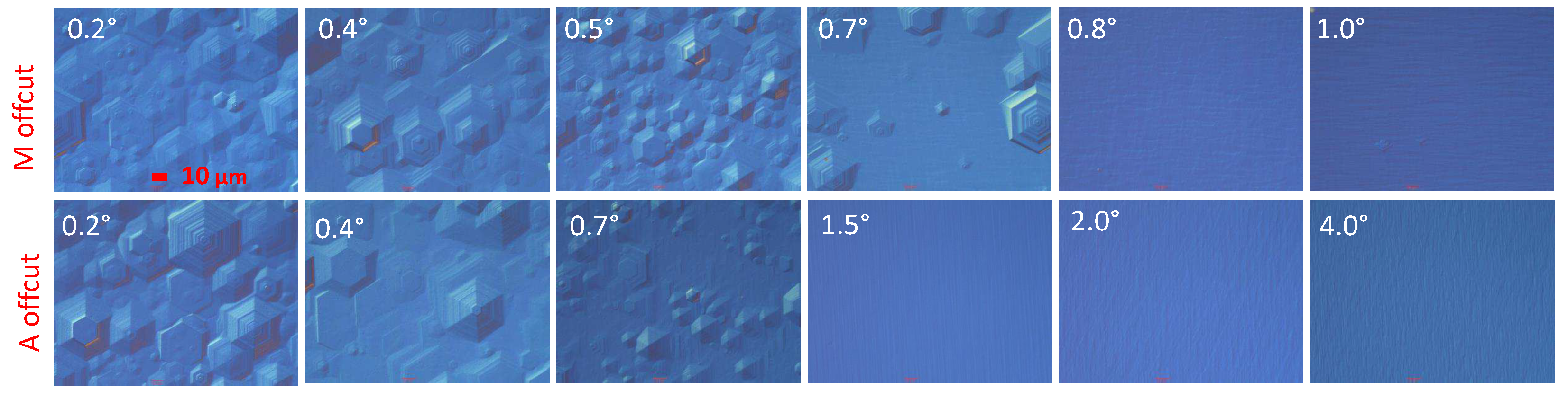
Figure 1 shows the surface of N-polar GaN layers after the simultaneous growth of ≈1.4 μ m in 45 min growth at 1200 °C with a V/III ratio of 1650 on sapphire wafers with various misorientations in the A or M direction. Under these conditions, flat surfaces have been obtained already for misorientation angles of 0.8° and higher.
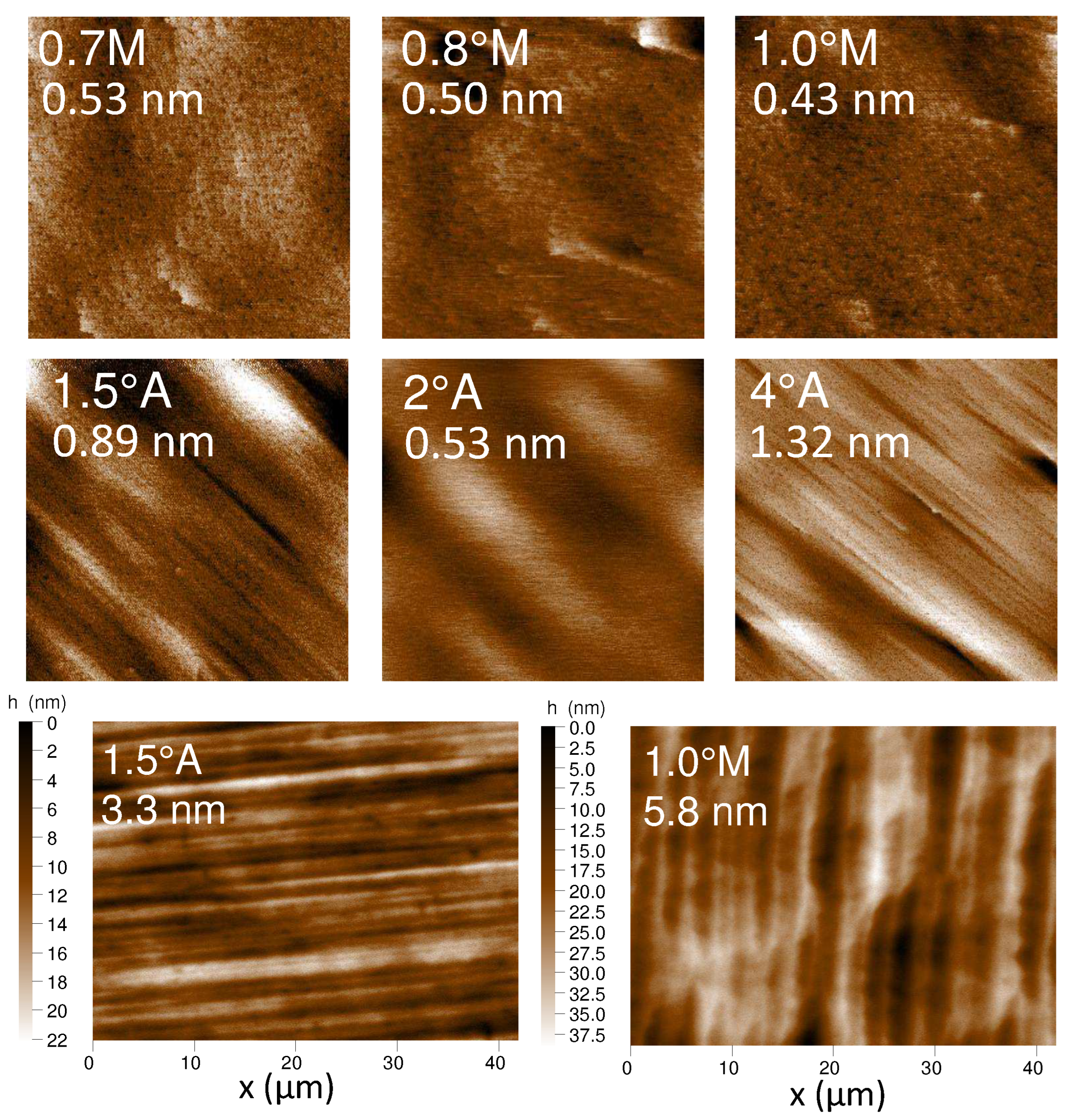
When looking at the surfaces using AFM in Figure 2, one can clearly see that under our conditions, the surfaces grown on sapphire with M misorientation had a generally lower root mean square roughnesses over 2 × 2 μ m 2 than the ones along A. There is, however, a large-scale waviness on the M misorientation samples that leads to higher roughnesses when measured over larger areas (e.g., 8–9 nm for 1°M over 465 μ m × 350 μ m compared to 2–3 nm for 2°A) as reported before [4,5].
In addition to the different roughness, there is also a different morphology. The wafer flats (sapphire a-plane) were at 45°. Thus, the step edges should run at 45° on M misorientations (top row in Figure 2) and −45° on A (middle row in Figure 2). However, the steps are not very visible for M misorientation in the top row. Our explanation is that when the step-edges are parallel to the GaN m-plane (as on A misorientation), they are straight and visible. However, when the step-edges run along the a-plane, they become unstable and instead form a zig-zag of different equivalent m-planes, which causes the larger waviness. This is more clearly seen in the large-area surface maps in Figure 2 bottom, again very straight steps from 1.5°A and a strong meandering of steps and higher RMS roughness for 1°M.
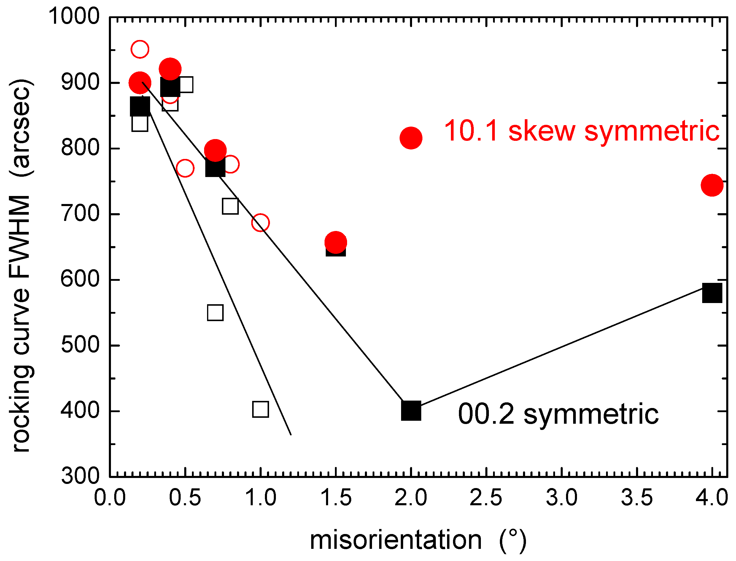
The morphology is also reflected in the XRD rocking curves FWHM in Figure 3; the smoother a sample, the narrower the 0002 FWHM becomes. When the HHLs vanish, the FWHM reduces from 700–900″ to ≈400–550″. The reason is that the HHLs all have a slightly different twist and tilt. Hence, a coalesced sample without HHLs has larger-sized domains with similar twist and tilt and thus less broadening. However, the XRD FWHMs increase again together with the RMS roughness at 4°A misorientation, which is probably due to the very pronounced step-bunching reducing again the average domain size.
Thus, for our growth condition, we found that sapphire misorientations along the m-direction result in smoother surfaces in small scales with narrower XRD FWHM. Smooth surfaces were obtained for misorientations as low as 0.8°, which is less than what had been previously reported. Apparently, the growth conditions are most important in order to obtain smooth N-polar surfaces and with them a good crystal quality.

3.2. Impact of Growth Conditions

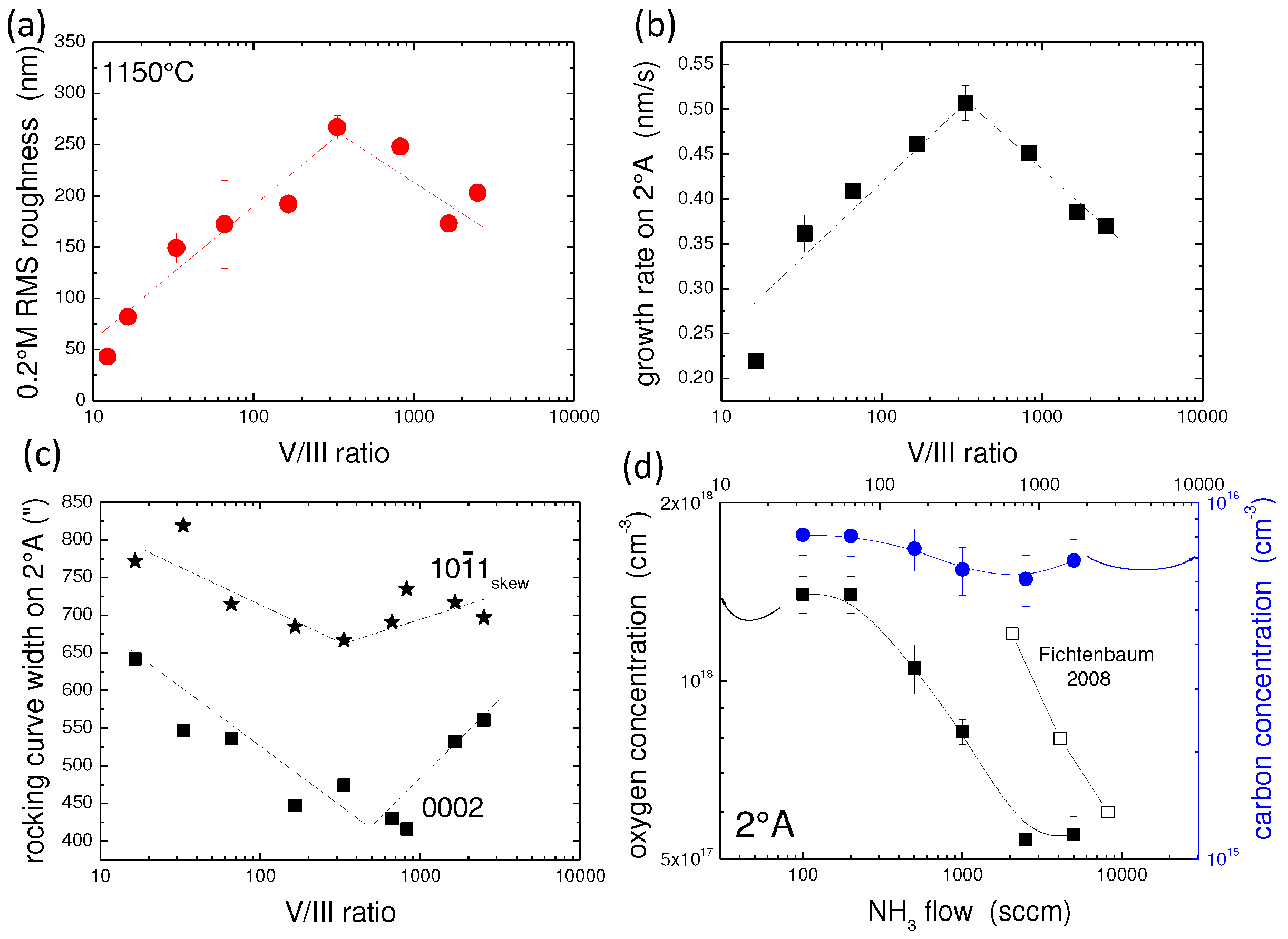
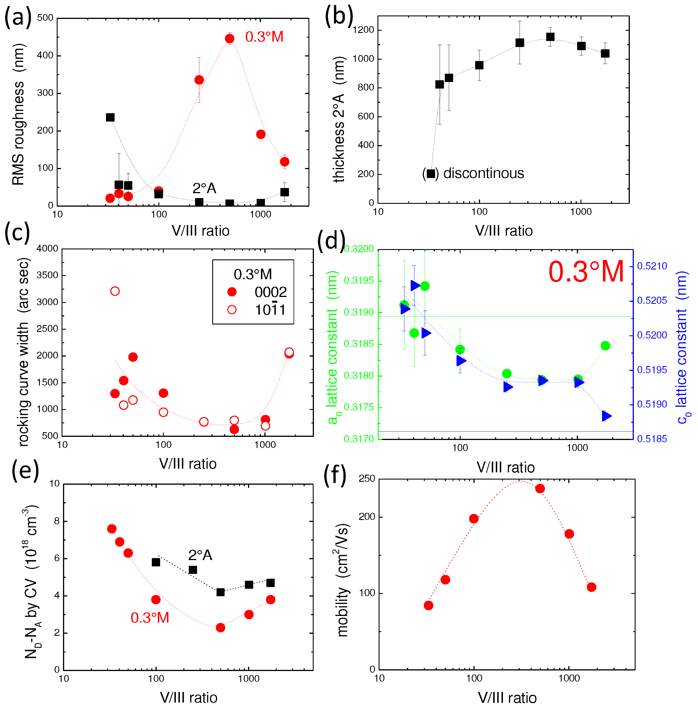
Therefore, we investigated the impact of growth conditions, essentially the variation of the NH 3 flow. For this, we used 2°A sapphire together with 0.3°M or 0.2°M. There were two series with a nominal growth rate of 0.45 nm/s at 1150 °C and a second using a 1.5× higher TMGa flow at 1180 °C to obtain smoother surfaces at low misorientations. For each of the series, the ammonia flow was changed and all other parameters were kept constant.
Even to the naked eye, the surfaces of the N-polar GaN on the 0.3°M change strongly in Figure 4. There are two trends visible. At high V/III ratios (above 500), the HHLs became smaller, and additional smaller HHLs appear. Thus, the height differences and with it the RMS roughness decrease. Below 500, the tops of the HHLs become first flatter and then rounder until at a V/III ratio of 33 just some <50 nm high pancake-like structures remain on 0.3°M at 1180 °C. The same but a little weaker is observed on 0.2°M, too.
In comparison, the GaN surfaces grown on 2°A sapphire remained flat for almost all conditions with an average RMS roughness of ( 0.7 ± 0.15 ) nm. The waviness only increased at the lowest and highest V/III ratio, which is in reverse to the trend for the 0.2°M and 0.3°M surfaces.
Figure 5 shows the same trend in numbers for the growth at 1150 °C. The roughness on 0.2°M sapphire and the growth rate on 2°A correlate nicely; both increase with the increasing V/III ratio until 500. At higher V/III ratios, the overall roughness and the growth again rate decrease. The XRD FWHM instead decreases until a V/III ratio of 500 and then increases again.
The same reversal of trends at a V/III ratio of about 500 is seen in Figure 6 for the growth with a higher TMGa flow at 1180 °C on 0.3°M and 2°A sapphire. At this high temperature, the GaN layer grown on the 2°A sapphire substrates developed larger holes at V/III ratios below 100 and thus, XRD and electrical measurements were not reliable, and only partial data are available for 2°A. Nevertheless, the trends reverse for nearly all parameters at a V/III ratio of around 500, which is similar to the 1150 °C growth series. The growth rate first increases and then decreases with the increasing V/III ratio, the XRD rocking curve FWHM first decreases and then increases, and there is an opposite trend in RMS roughness between low and 2°A misorientation with either maximum respective minimum at V/III ratios of 500. A reversal of trends was also found in the PL data, which is discussed in the next Section 3.3.
At first glance, it seems surprising that the XRD FWHM for samples with hillocks (Figure 6c) and with a smooth surface on 2°A (Figure 5c) show exactly the same trends despite a reverse trend in RMS roughness (Figure 5a and Figure 6a). However, for the GaN hetero-epitaxy, the initially high dislocation densities are reduced by a 3D growth phase at the onset of buffer growth, where dislocations are bent towards each other and can annihilate. Too long diffusion lengths (at very low V/III ratios) lead to a very quick coalescence and thus to a very short 3D growth phase with many remaining dislocations. Hence, a surface with a long and strong 3D growth phase is the one with the lowest number of dislocations and thus the one with the smallest XRD FWHM. For low misorientations, this results in the largest HHLs.
The initial increase of the growth rate with increasing V/III ratio can be explained by the effect of a reduced Ga desorption with increased NH 3 flow. Since the Ga species stay a shorter time on the surface until they meet with NH 3 , the probability of desorption decreases compared to incorporation. Shorter times on the surface with increasing NH 3 flow also translates into shorter diffusion lengths, which increases the 3D growth that is essential for dislocation annihilation, as discussed above. Thus, the XRD FWHM reduces too with the increasing V/III ratio. However, the reversal of trends starting at V/III ratio of 300 shows that there is more at work than supersaturation alone.
One way to understand this would be a change of the surface termination. On an ideal (000 1 - ) surface, nitrogen is bound with three bonds downwards, while Ga has three upwards dangling bonds and is bound with just a single bond. However, this surface is not the most stable structure. According to DFT calculations, there are two more stable surfaces on N-polar (000 1 - ) GaN: a Ga-adlayer at Ga-rich conditions and a N-terminated 3N-H ( 2 × 2 ) surface at N-rich conditions [15]. The N-polar Ga-adlayer surface has only half the energy barrier for oxygen adsorption compared to the Ga-polar Ga-adlayer surface [16] and thus will incorporate much more oxygen than the Ga-polar (0001) Ga-adlayer surface, leading to a very high oxygen background at lower V/III ratios. On the other hand, all adsorption sites on the 3N-H ( 2 × 2 ) surface are Ga sites, which makes oxygen incorporation more difficult since oxygen would prefer a nitrogen site. Furthermore, it seems likely that oxygen reaching the 3N-H ( 2 × 2 ) surface rather reacts with the adsorbed hydrogen and should further reduce oxygen incorporation.
Therefore, we assume that at low V/III ratios, a Ga-adlayer covers the entire N-polar surface. However, when increasing the V/III ratio above 300, domains of the N-rich 3N-H ( 2 × 2 ) surface would appear as well and grow in size, until at V/III ratios above 2000, at which point the N-rich 3N-H ( 2 × 2 ) would cover the entire surface. The change of the dominating surface would affect the adsorption and desorption probabilities of oxygen and Ga. The oxygen incorporation would reduce from the high value of the Ga-adlayer at V/III ratios below 300 to the low value of the 3N-H ( 2 × 2 ) for V/III ratios above 2000. Indeed, the data in Figure 5d) show a high value for low V/III ratios and then a strong reduction for the V/III ratio between 300 and 2000 to a constant low value.
The growth rate is more complex, since it overlaps with the thermodynamic effect of NH 3 on Ga surface lifetimes and Ga desorption as discussed above. Furthermore, no calculated data on Ga adsorption exists. However, a N-terminated surface such as the 3N-H ( 2 × 2 ) means that Ga can adsorb only with a single bond compared to three bonds on a Ga-adlayer surface. Moreover, the mixed N/hydrogen termination of the 3N-H ( 2 × 2 ) surface means that even the dangling bonds are most often saturated by hydrogen. Together, it is reasonable to assume a lower Ga adsorption probability on the 3N-H ( 2 × 2 ) surface. Then, the adsorption probability of Ga would start to reduce above a V/III ratio of 300 with the increasing 3N-H ( 2 × 2 ) coverage. This reduction compensates for the increase from shorter surface lifetimes of Ga with increased NH 3 flow. With the increasing V/III ratio, the growth rate reduces with increasing 3N-H ( 2 × 2 ) area until at V/III ratios above 2000, only the N-rich 3N-H ( 2 × 2 ) surface covers everything. For higher V/III ratios, the growth rate should stay constant, and indeed, the last point of Figure 5 at the maximum possible V/III ratio of 2800 is changing less than the trend line.
The simultaneous presence of domains with two different surfaces at the same time should also shorten the diffusion length because of the high number of dangling bonds at the border of a domain. Thus, the diffusion length is at a minimum between 500 and 1000, where the coverage with either surface would be equal. The diffusion length would increase again with higher V/III ratios until the whole surface is only covered by the 3N-H ( 2 × 2 ) surface. Further increasing the V/III ratio should again decrease the diffusion length due to a reduced surface lifetime with more incoming N-species, but this was not possible with the given TMGa flow rates. The increasing diffusion length between the V/III ratios of 500 and 2000 due to the larger single surface domains could explain the smaller and denser HHLs on low misorientations (Figure 4 top and middle) and the increasing XRD FWHM at very high V/III ratios (Figure 5c) and Figure 6c due to weaker 3D growth as the 3N-H ( 2 × 2 ) domain size increases.
To summarize our model: at lower V/III ratios, the surface is entirely Ga-adlayer terminated, and the oxygen incorporation is at maximum. Since the Ga diffusion length equals the time to meet a N species to incorporate, the Ga diffusion length increases with the decreasing V/III ratio. However, a longer Ga diffusion length also means that the mobile Ga rests on the surface for longer, thus increasing the probability of Ga desorption. Hence, the growth rate decreases with decreasing V/III ratios until for very low V/III ratios below 30, the growth becomes N-limited and the growth rate drops sharply (below V/III = 40 in Figure 5b and Figure 6b). When increasing the V/III ratio above 300, domains of the 3N-H ( 2 × 2 ) surface start to appear. This 3N-H ( 2 × 2 ) surface has a much lower probability of oxygen incorporation, and thus, the residual oxygen starts to decrease with increasing 3N-H ( 2 × 2 ) coverage (Figure 5d). In addition, Ga adsorption is reduced on the 3N-H ( 2 × 2 ) surface, reducing the growth rate with increasing 3N-H ( 2 × 2 ) coverage with increasing V/III ratio. At the same time, the presence of two different surfaces strongly reduces the Ga diffusion length due to a high probability of nucleation at domain boundaries and enhances the initial 3D growth phase, leading to a minimum in XRD FWHM and a maximum in HHL sizes on low misorientations at V/III ratios around 500. Increasing the V/III ratio further reduces the Ga-adlayer surface area until only the 3N-H ( 2 × 2 ) surface covers everything for V/III ratios above 2000. Until this point, the oxygen incorporation and growth rate decrease, the Ga diffusion length increases again, the FWHM increases (due to less 3D growth), and the HHLs sizes decrease again.
It must be emphasized that the conditions for reaching a nitrogen-terminated surface depend not only on the TMGa and NH 3 flow rates but also on the reactor design. Consequently, the V/III ratio where the 3N-H ( 2 × 2 ) surface dominates (and thus, the oxygen incorporation has reached its minimum) differs a lot among the literature judging from the reported oxygen incorporation [2,8,9,10]. Even for our two series at 1150 °C and 1180 °C, the value of the turning point at 500 was rather a coincidence: the higher temperatures and thus higher NH 3 decomposition was offset by the higher growth rate for the second series.

3.3. Optical Properties of N-Polar GaN

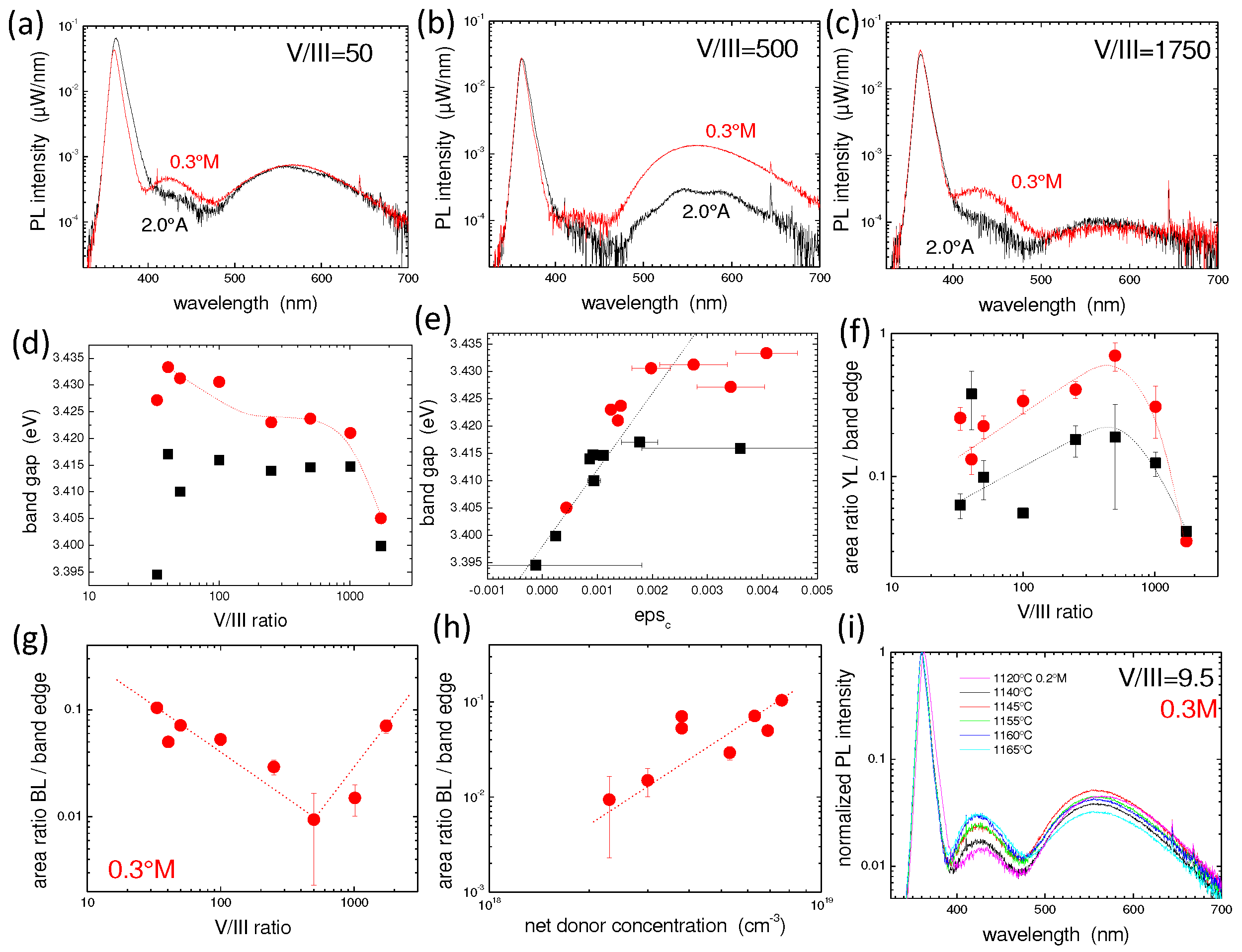
The room-temperature photoluminescence data are complex. Figure 7 shows three typical spectra at the low (50) (a), trend reversal (500) (b) and highest (1750) (c) V/III ratio for the 1180 °C series. Most striking is a strong shift of the band edge for the low miscut samples; see Figure 7d. The shift of the band edge is mostly related to strain, since the different surface morphologies (smooth versus HHLs) resulted in a different strain, as confirmed in Figure 7e: the shift of the band edge follows nicely the strain along [0001]. The slope of the dotted line is 14 eV which is between the literature values for the Ga polar GaN of 12 eV [17] and 15.4 eV [18]. However, at low V/III ratios (and high carrier concentrations), other effects such as band filling may additionally shift the bands to even lower values and cause a deviation from the strain-related shift.
The yellow luminescence band (YL) in Figure 7f is the highest in relation to the band edge at the V/III ratio of 500. This was independent of the surface roughness; similar trends were observed for 2°A and 0.2°M/0.3°M despite their opposite trends in roughness. This would indicate that the YL is unrelated to HHLs. Following our assumption of a surface transition around this V/III ratio, then the YL could be related to a defect from domain boundaries at each surface. Carbon alone is unlikely to cause the YL, since the carbon background is low (<10 16 cm 2 ) and is almost not changing with the V/III ratio (Figure 5d). Furthermore, the XRD FWHM is at minimum at the highest YL (Figure 5c and Figure 6c), ruling out a connection with extended structural defects or dislocations. This is quite different from the behaviour of Ga-polar GaN where a high YL is usually associated with carbon-related complexes and poor crystal quality.
The YL of our samples is centred around 2.2 eV (570 nm) which according to a recent report for the molecular beam epitaxy of N-polar GaN might be related to Gallium vacancies [19]. However, there are reports of YL of N-polar GaN related with carbon. After very high C- and O-implantation into N-polar GaN, the YL only increased with C-implantation [20]. Moreover, a strong YL for N-polar GaN growth using Na-flux was correlated with high carbon incorporation [21]. The same report noted that the YL was shifted to longer wavelengths for N-polar GaN [21], while the YL shifted with heavy carbon implantation to slightly shorter values around 550 nm [20]. Given the very low carbon incorporation for V/III ratios as low as 100 (Figure 5d), which is typical for N-polar GaN MOVPE growth [2,9], for our series, a direct correlation of carbon and YL seems unlikely. The best explanation seems that there is more than one complex active in the same energy range, and Ga vacancies would agree with an increasing YL due to growth on a disordered surface with two simultaneous terminations.
There is further evidence for a different active complex. Figure 7a–c also show a second band centred at 430 nm (hence, blue luminescence band, BL) for the 0.3°M (and 0.2°M) samples, which is most prominent at the lowest and highest V/III ratios. This BL is barely visible on the higher misorientations (and thus smoother surfaces) and thus was often hidden in the donor–acceptor-related transitions with phonon replicas close to the band edge [2,22]. However, a strong BL was reported on N-polar GaN with many HHLs [23]. In another series of samples at lower growth temperatures and even lower V/III ratios, the BL increased with increasing growth temperatures (Figure 7i).
Moreover, the BL anticorrelates with the YL and the roughness but correlates with the net donor concentration (Figure 7h). An early publication suggested indeed a higher carbon incorporation with HHLs on N-polar GaN [8] and speculated that the apex of the HHLs could favour carbon incorporation. In a recent report, a BL at 430 nm can be observed to increase after heavy carbon implantation and annealing of N-polar GaN (Figure 5 in [20]). Finally, on Ga-polar GaN, the blue luminescence is related to carbon [24].
Since the BL increases in intensity with growth temperature and carrier concentration, we speculate that the BL might probably come from electrically active carbon incorporated on a Ga site or maybe an interstitial. However, the low-carbon background makes this questionable, and more data are needed.

3.4. Smooth N-Polar GaN with Low Misorientation

As shown in Section 3.1, misorientations in m-directions are favourable to reduce HHLs at low misorientations. Since typical (0001) sapphire substrates are usually misoriented along this direction, we used 0.2°M and 0.3°M in our study as well.
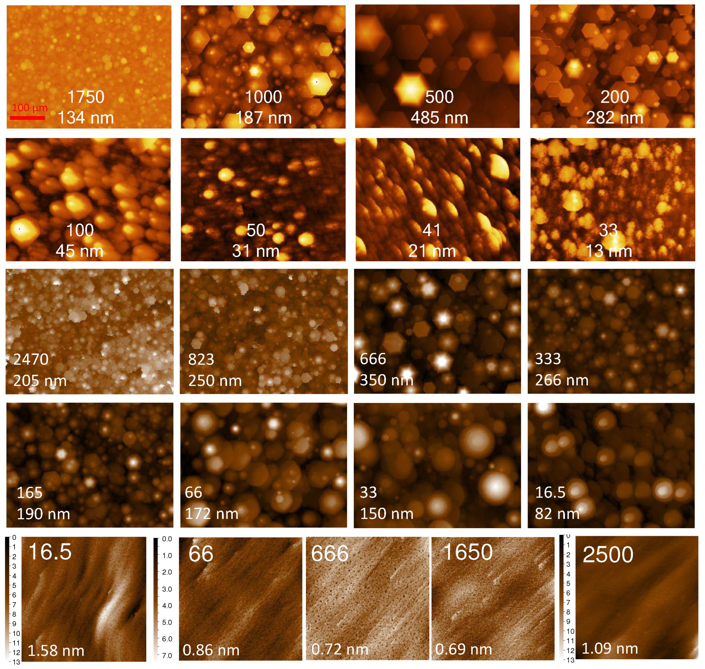
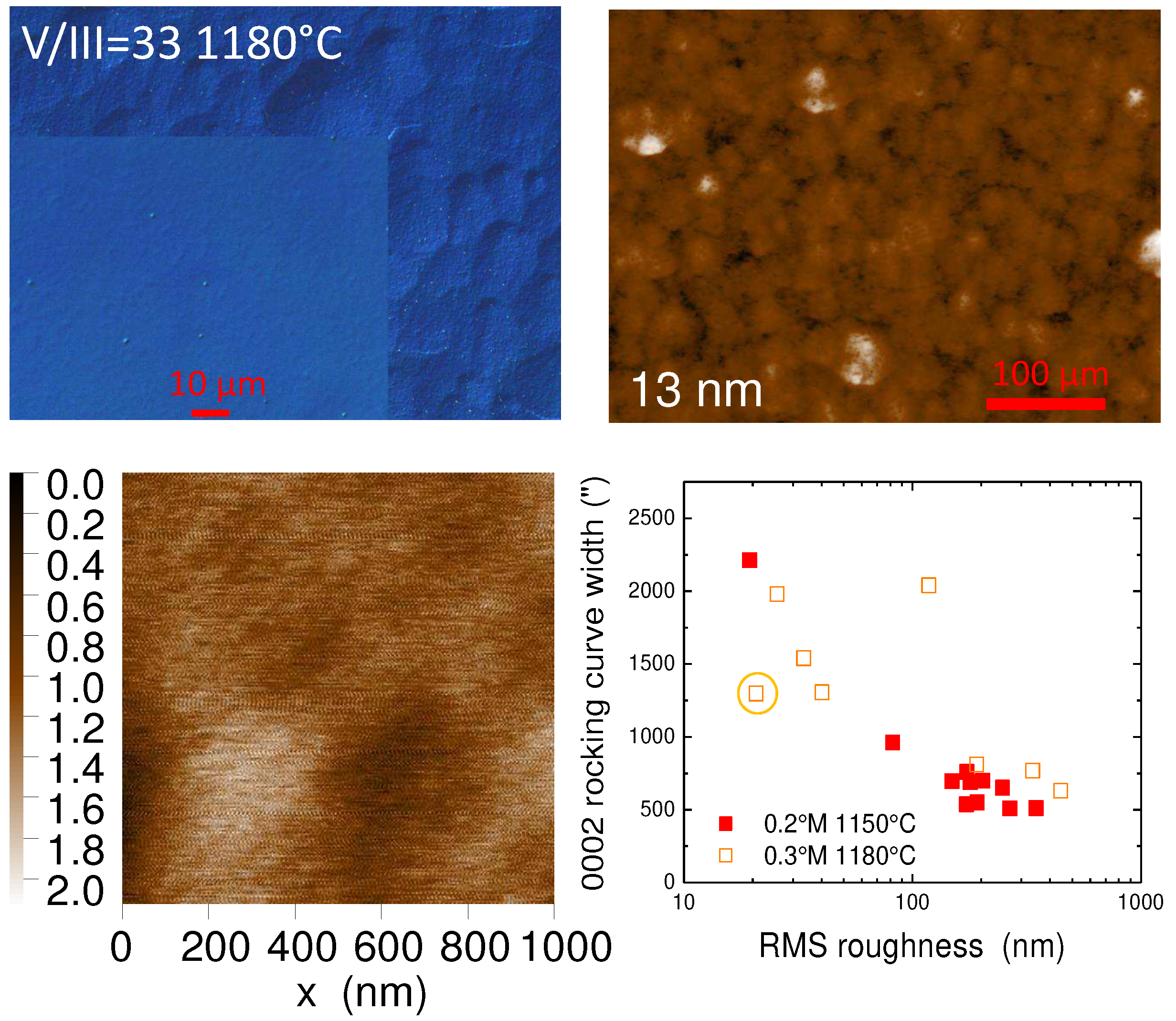
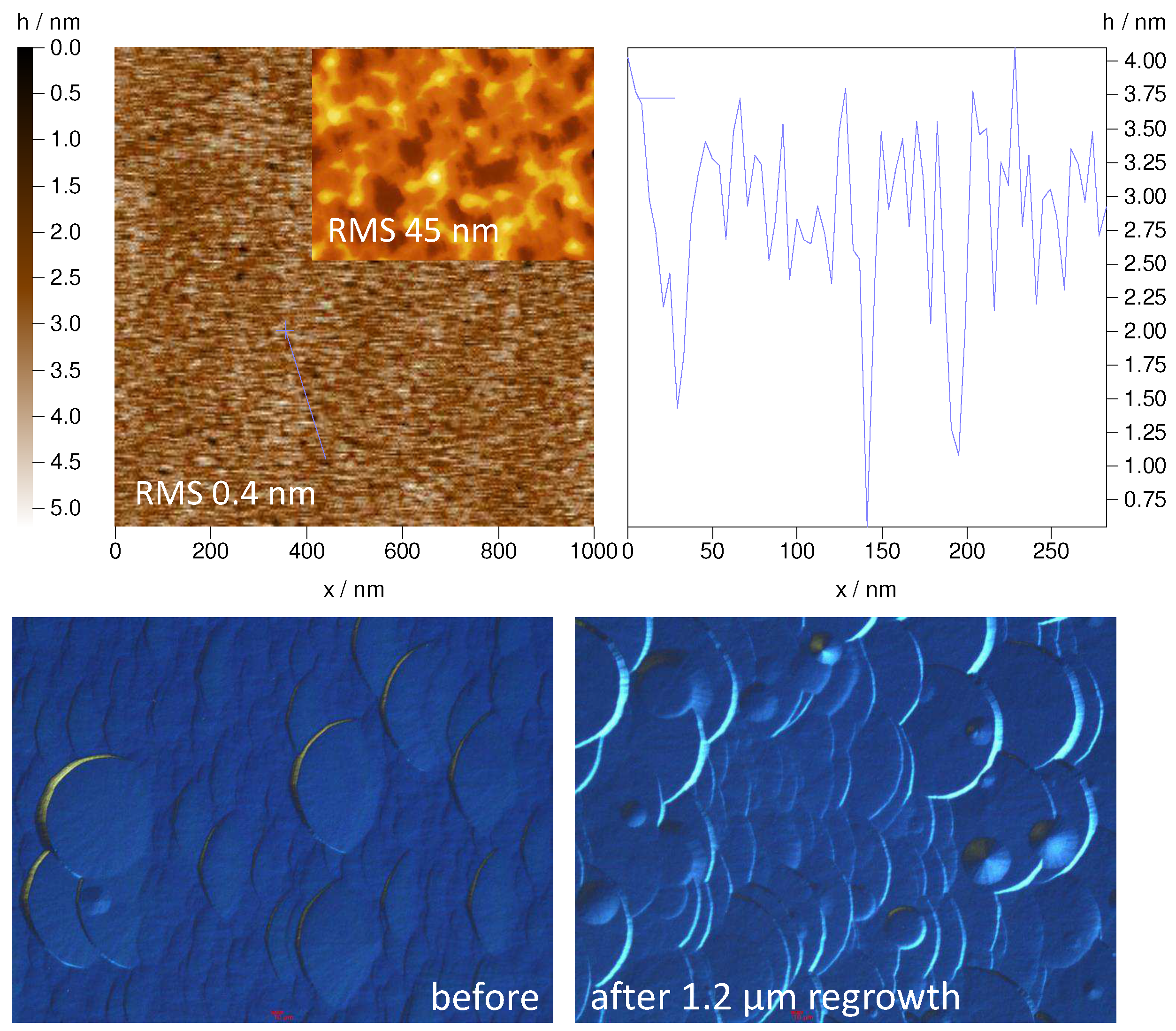
The best sample from these series is shown in Figure 8, which was obtained deep in the desorption-limited growth regime at the stability edge of even N-polar GaN. (Ga-polar GaN layers were completely desorbed at the conditions within a few minutes.) The large area RMS roughness is 13 nm, which is three to four times higher than for typical GaN surfaces (4–6 nm) but could be still accepted for devices. Moreover, the surface of this sample shows even some traces of atomic steps. This was the only, low misorientation N-polar GaN surface where we have ever seen step edges. Typically, the surfaces are featureless with 1 nm deep holes such as the surface shown in Figure 9.
However, the smooth surface comes with a price. As shown, in the bottom right of Figure 8, the XRD 0002 ω rocking curve FWHM strongly increases when the RMS roughness decreases. This decrease of crystal quality is due to a lack of 3D growth, i.e., the layer coalesces too fast, and the dislocations do not have enough time to bend sidewards and cannot annihilate.
Hence, we have tried a multi-step approach for the high-temperature growth of N-polar GaN. The first step was with a high V/III ratio to start with many nuclei. In the next step, the layer is smoothed by overgrowth with a very low V/III ratio. By this, reasonable flat surfaces with acceptable XRD FWHM around 700–900 arcsec have been achieved. Figure 9 shows a typical resulting surface. The surface does not show atomic steps. Instead, there are many 1–2 nm deep holes. Such a morphology has been reported before for N-polar GaN [25]. The density of the holes is in the 10 9 10 10 cm 3 range and thus might be related to dislocations.
There remains another challenge: While somewhat flat and with not too bad crystal quality, these layers had high background carrier concentrations. Thus, we tried regrowth on these surfaces with the optimised V/III ratio of 1000. This must be performed in a third step because half of the sample thickness was desorbed when heating to 1180 °C for the regrowth.
The third layer has lower carrier densities close to 10 18 cm 3 . However, small HHLs reappear on its surface, as in Figure 9 bottom right. The density of these small HHLs is 1–2 × 10 4 cm 2 with a height of 20–40 nm after 30 min of regrowth. Due to the above-discussed strong GaN desorption before the start of the regrowth, we have not systematically studied their shapes as a function of growth time.
Therefore, it is possible to obtain a smooth N-polar GaN with decent structural quality on low misorientation. However, it seems very challenging to also obtain a low background carrier concentration.

4. Conclusions

We have investigated the growth of N-polar GaN and found that in our reactor, around a V/III ratio of 500, the growth rate, crystal quality, surface roughness and impurity incorporation change trends. This is consistent with a change from a mainly Ga-terminated surface to an N-terminated surface since the latter offers fewer, more loosely bonded adsorption sites due to its lone upwards dangling bond. We have obtained nice quality N-polar surfaces on misorientations in [1 1 - 00] for as low as 0.8° using 50–100 °C higher temperatures than (0001) Ga-polar growth and V/III ratios of 1000. Obtaining smooth N-polar surfaces with lower standard misorientations is possible using very low V/III ratios in a multi-step approach but leads to high background impurity incorporation. According to our results, the lowest misorientations of sapphire for a single-step growth would be 0.8° to 1° along [1 1 - 00] (m-directions).

Author Contributions

Conceptualization, P.P.; Data curation, M.P., I.F. and P.P.; Investigation, M.P., I.F. and P.P.; Writing—original draft, M.P.; Writing—review and editing, M.P. and P.P. All authors have read and agreed to the published version of the manuscript.

Funding

This project has received funding from the European Union’s Horizon 2020 research and innovation program under the Marie Skłodowska-Curie grant agreement No. 898704.

Data Availability Statement

The data presented in this study are available on request from the corresponding author. The data are not publicly available due to some of it being in a proprietary format and needing special software.

Conflicts of Interest

The authors declare no conflict of interest.

Abbreviations

The following abbreviations are used in this manuscript:
HHLHexagonal Hillock
XRDX-ray Diffraction
FWHMFull Width at Half Maximum
AFMAtomic Force Microscopy
PLPhotoluminescence
SIMSSecondary Ion Mass Spectroscopy
YLYellow Luminescence Band
BLBlue Luminescence Band

References

  1. Leung, B.; Sun, Q.; Yerino, C.D.; Han, J.; Coltrin, M.E. Using the kinetic Wulff plot to design and control nonpolar and semipolar GaN heteroepitaxy. Semicond. Sci. Technol. 2012, 27, 024005. [Google Scholar] [CrossRef]
  2. Keller, S.; Li, H.; Laurent, M.; Hu, Y.; Pfaff, N.; Lu, J.; Brown, D.F.; Fichtenbaum, N.A.; Speck, J.S.; DenBaars, S.P.; et al. Recent progress in metal-organic chemical vapor deposition of N-polar group-III nitrides. Semicond. Sci. Technol. 2014, 29, 113001. [Google Scholar] [CrossRef]
  3. Zauner, A.R.A.; Weyher, J.; Plomp, M.; Kirilyuk, V.; Grzegory, I.; van Enckevort, W.J.P.; Schermer, J.J.; Hageman, P.R.; Larsen, P.K. Homo-epitaxial GaN growth on exact and misoriented single crystals: Suppression of hillock formation. J. Cryst. Growth 2000, 210, 435–443. [Google Scholar] [CrossRef]
  4. Keller, S.; Fichtenbaum, N.A.; Wu, F.; Brown, D.; Rosales, A.; DenBaars, S.P.; Speck, J.S.; Mishra, U.K. Influence of the substrate misorientation on the properties of N-polar GaN films grown by metal organic chemical vapor deposition. J. Appl. Phys. 2007, 102, 083546. [Google Scholar] [CrossRef]
  5. Su, Z.; Li, Y.; Hu, X.; Song, Y.; Kong, R.; Deng, Z.; Ma, Z.; Du, C.; Wang, W.; Jia, H.; et al. N-polar GaN Film Epitaxy on Sapphire Substrate without Intentional Nitridation. Materials 2022, 15, 3005. [Google Scholar] [CrossRef]
  6. Sumiya, M.; Yoshimura, K.; Ito, T.; Ohtsuka, K.; Fuke, S.; Mizuno, K.; Yoshimoto, M.; Koinuma, H.; Ohtomo, A.; Kawasaki, M. Growth mode and surface morphology of a GaN film deposited along the N-face polar direction on c-plane sapphire substrate. J. Appl. Phys. 2000, 88, 1158–1165. [Google Scholar] [CrossRef]
  7. Mita, S.; Collazo, R.; Rice, A.; Tweedie, J.; Xie, J.; Dalmau, R.; Sitar, Z. Impact of gallium supersaturation on the growth of N-polar GaN. Phys. Status Solidi 2011, 8, 2078–2080. [Google Scholar] [CrossRef]
  8. Sumiya, M.; Yoshimura, K.; Ohtsuka, K.; Fuke, S. Dependence of impurity incorporation on the polar direction of GaN film growth. Appl. Phys. Lett. 2000, 76, 2098–2100. [Google Scholar] [CrossRef]
  9. Fichtenbaum, N.; Mates, T.; Keller, S.; DenBaars, S.; Mishra, U. Impurity incorporation in heteroepitaxial N-face and Ga-face GaN films grown by metalorganic chemical vapor deposition. J. Cryst. Growth 2008, 310, 1124–1131. [Google Scholar] [CrossRef]
  10. Tanikawa, T.; Kuboya, S.; Matsuoka, T. Control of impurity concentration in N-polar (000 1 - ) GaN grown by metalorganic vapor phase epitaxy. Phys. Status Solidi (B) 2017, 254, 1600751. [Google Scholar] [CrossRef]
  11. Szymanski, D.; Wang, K.; Kaess, F.; Kirste, R.; Mita, S.; Reddy, P.; Sitar, Z.; Collazo, R. Systematic oxygen impurity reduction in smooth N-polar GaN by chemical potential control. Semicond. Sci. Technol. 2021, 37, 015005. [Google Scholar] [CrossRef]
  12. Mohn, S.; Stolyarchuk, N.; Markurt, T.; Kirste, R.; Hoffmann, M.P.; Collazo, R.; Courville, A.; Di Felice, R.; Sitar, Z.; Vennéguès, P.; et al. Polarity Control in Group-III Nitrides beyond Pragmatism. Phys. Rev. Appl. 2016, 5, 054004. [Google Scholar] [CrossRef] [Green Version]
  13. Lin, Y.; Sena, H.; Frentrup, M.; Pristovsek, M.; Honda, Y.; Amano, H. Stress relaxation of AlGaN on nonpolar m-plane GaN substrate. J. Appl. Phys. 2023, 133, 225702. [Google Scholar] [CrossRef]
  14. Kusch, G.; Frentrup, M.; Hu, N.; Amano, H.; Oliver, R.A.; Pristovsek, M. Defect characterization of 10 1 - 3 GaN by electron microscopy. J. Appl. Phys. 2022, 131, 035705. [Google Scholar] [CrossRef]
  15. Akiyama, T.; Nakane, H.; Uchino, M.; Nakamura, K.; Ito, T. Structures and Polarity of III-Nitrides: Phase Diagram Calculations Using Absolute Surface and Interface Energies. Phys. Status Solidi (B) 2018, 255, 1700329. [Google Scholar] [CrossRef]
  16. Sun, Q.; Selloni, A.; Myers, T.H.; Doolittle, W.A. Oxygen adsorption and incorporation at irradiated GaN(0001) and GaN(000 1 - ) surfaces: First-principles density-functional calculations. Phys. Rev. B 2006, 74, 195317. [Google Scholar] [CrossRef]
  17. Amano, H.; Hiramatsu, K.; Akasaki, I. Heteroepitaxial Growth and the Effect of Strain on the Luminescent Properties of GaN Films on (11 2 - 0) and (0001) Sapphire Substrates. Jpn. J. Appl. Phys. 1988, 27, L1384. [Google Scholar] [CrossRef]
  18. Shikanai, A.; Azuhata, T.; Sota, T.; Chichibu, S.; Kuramata, A.; Horino, K.; Nakamura, S. Biaxial strain dependence of exciton resonance energies in wurtzite GaN. J. Appl. Phys. 1997, 81, 417–424. [Google Scholar] [CrossRef]
  19. Tatarczak, P.; Turski, H.; Korona, K.P.; Grzanka, E.; Skierbiszewski, C.; Wysmołek, A. Optical properties of N-polar GaN: The possible role of nitrogen vacancy-related defects. Appl. Surf. Sci. 2021, 566, 150734. [Google Scholar] [CrossRef]
  20. Zhao, Y.; Xu, S.; Feng, L.; Lin, Z.; Li, P.; Zhang, J.; Hao, Y. The Yellow Luminescence Origin of N-Polar GaN Film Grown by Metal Organic Chemical Vapor Deposition. ECS J. Sol. State Sci. Technol. 2020, 9, 056003. [Google Scholar] [CrossRef]
  21. Si, Z.; Liu, Z.; Zheng, S.; Dong, X.; Gao, X.; Wang, J.; Xu, K. Yellow luminescence and carrier distribution due to polarity-dependent incorporation of carbon impurities in bulk GaN by Na flux. J. Lumin. 2023, 255, 119566. [Google Scholar] [CrossRef]
  22. Masui, H.; Keller, S.; Fellows, N.; Fichtenbaum, N.A.; Furukawa, M.; Nakamura, S.; Mishra, U.K.; DenBaars, S.P. Luminescence Characteristics of N-Polar GaN and InGaN Films Grown by Metal Organic Chemical Vapor Deposition. Jpn. J. Appl. Phys. 2009, 48, 071003. [Google Scholar] [CrossRef]
  23. Kirste, R.; Collazo, R.; Callsen, G.; Wagner, M.R.; Kure, T.; Sebastian Reparaz, J.; Mita, S.; Xie, J.; Rice, A.; Tweedie, J.; et al. Temperature dependent photoluminescence of lateral polarity junctions of metal organic chemical vapor deposition grown GaN. J. Appl. Phys. 2011, 110, 093503. [Google Scholar] [CrossRef] [Green Version]
  24. Reshchikov, M.A. Fine Structure of the Carbon-Related Blue Luminescence Band in GaN. Solids 2022, 3, 231–236. [Google Scholar] [CrossRef]
  25. Sun, Q.; Suk Cho, Y.; Kong, B.H.; Koun Cho, H.; Shine Ko, T.; Yerino, C.D.; Lee, I.H.; Han, J. N-face GaN growth on c-plane sapphire by metalorganic chemical vapor deposition. J. Cryst. Growth 2009, 311, 2948–2952. [Google Scholar] [CrossRef]
Figure 1. Optical microscopy images of N-polar GaN growth on sapphire with different misorientation.
Crystals 13 01072 g001
Figure 2. The 2 μ m × 2 μ m AFM images of N-polar GaN growth on sapphire with different misorientation. The misorientation and the RMS roughness are given in the image. The z-scale is 4.5 nm for all images but 4°A where it is 10 nm. The wafer flat was always placed at 45°. The bottom row shows the large area surface of 1.5°A and 1°M. Clearly, the 1°M has a larger waviness along the step edges and a larger RMS roughness.
Crystals 13 01072 g002
Figure 3. XRD FHWM of the skew-symmetric 10 1 - 1 reflection (red) and the symmetric 0002 reflection (black) for sapphire misorientations along M (open symbols) and A (filled). The black lines are guides to the eye for the 0002 reflection on M and A misorientation.
Crystals 13 01072 g003
Figure 4. Top two rows: 465 μ m × 350 μ m white light holographic surface maps of N-polar GaN on 0.3°M grown for 30 min at 1180 °C with a decreasing NH 3 flow and constant TMGa flow. The first number indicates the V/III ratio and the second indicates the mean RMS roughness at these conditions. Middle two rows: 465 μ m × 350 μ m white light holographic surface maps of N-polar GaN on 0.2°M grown for 45 min at 1150 °C with a decreasing NH 3 flow and constant TMGa flow. The first number indicates the V/III ratio and the second indicates the mean RMS roughness at these conditions. Bottom row: 2 μ m × 2 μ m AFM images after growth for 45 min at 1150 °C on 2°A sapphire at very low, intermediate, and highest NH 3 flow.
Crystals 13 01072 g004
Figure 5. Result for NH 3 flow variation after 45 min growth at 1150 °C. (a) Surface roughness on 0.2°M sapphire from white light interferometry, (b) growth rate on 2°A sapphire (smooth surface), (c) XRD rocking curved width for the symmetric 0002 (square) and skew-symmetric 10 1 - 1 (star) reflections, (d) SIMS data for oxygen and carbon for a series with different V/III ratio on 2°A misoriented sapphire. For comparison, the oxygen background data of Fichtenbaum et al. [9] have been added.
Crystals 13 01072 g005
Figure 6. Result for NH 3 flow variation after 30 min of growth at 1180 °C using a higher TMGa flow on 0.3°M (red circle) and 2°A sapphire (black square). (a) Surface roughness from white light interferometry, (b) growth rate on 2°A sapphire (smooth surface), (c) XRD rocking curved width for the symmetric 0002 (filled circle) and skew-symmetric 10 1 - 1 (open circle) reflections for 0.3°M, (d) a 0 and c 0 lattice constant on 0.3°M (solid lines are relaxed values), (e) donor concentration estimated from etching CV profiling, and (f) mobility on 0.3°M. The GaN layer had holes on the 2°A sapphire at V/III ratios below 100. Hence, XRD and electrical measurements were not meaningful.
Crystals 13 01072 g006
Figure 7. Top row (ac): Room-temperature PL with excitation by a HeCd laser for three representative V/III ratios at 1180 °C growth temperature, red for 0.3°M and black for 2°A. Middle row: (d) band gap over V/III ratio and (e) band gap over strain along [0001]. The dotted line has a slope of 14 eV. (f) Area ratio of band edge to yellow luminescence at 570 nm with an FWHM of ≈120 nm. Bottom row: Area ratio of GaN band edge to blue luminescence blue at 430 nm with an FWHM of ≈50 nm over (g) V/III ratio and (h) net donor concentration from C/V measurements, and (i) Room-temperature normalised PL for a series grown at different temperatures.
Crystals 13 01072 g007
Figure 8. Top row: 10 × Nomarski microscopy image with 100 × inset (left) and 465 μ m × 350 μ m white light holographic surface map (right). Bottom row: 1 × 1 μ m AFM image (left) and 0002 XRD reflection FWHM over large area roughness for all low misorientation samples (right). The sample shown in this figure is marked by a circle.
Crystals 13 01072 g008
Figure 9. Top row: The AFM image of the surface after two-step growth at V/III of 500 and 12 at 1150 °C on 0.2°M. This inset shows a 930 μ m × 700 μ m white light holography surface image. Bottom row: Nomarski images before and after regrowth at 1180 °C with 1 µm at a V/III ratio of 1000.
Crystals 13 01072 g009
Disclaimer/Publisher’s Note: The statements, opinions and data contained in all publications are solely those of the individual author(s) and contributor(s) and not of MDPI and/or the editor(s). MDPI and/or the editor(s) disclaim responsibility for any injury to people or property resulting from any ideas, methods, instructions or products referred to in the content.

