Article

Study of Magnesium Activation Effect on Pinch-Off Voltage of Normally-Off p-GaN HEMTs for Power Applications

by
Giovanni Giorgino
1,2,*,
Giuseppe Greco
3,
Maurizio Moschetti
1,
Cristina Miccoli
1,
Maria Eloisa Castagna
1,
Cristina Tringali
1,
Patrick Fiorenza
3,
Fabrizio Roccaforte
3 and
Ferdinando Iucolano
1
1
STMicroelectronics, Stradale Primosole n. 50, 95121 Catania, Italy
2
Dipartimento di Ingegneria “Enzo Ferrari”, University of Modena and Reggio Emilia, Via P. Vivarelli 10, 41125 Modena, Italy
3
Consiglio Nazionale delle Ricerche, Istituto per la Microelettronica e Microsistemi (CNR-IMM), Strada VIII n. 5, Zona Industriale, 95121 Catania, Italy
*
Author to whom correspondence should be addressed.
Crystals 2023, 13(9), 1309; https://doi.org/10.3390/cryst13091309
Submission received: 24 July 2023 / Revised: 12 August 2023 / Accepted: 25 August 2023 / Published: 27 August 2023
(This article belongs to the Special Issue Wide-Bandgap Semiconductors)

Abstract

:
The role of the magnesium (Mg) doping and its electrical activation on the off-state of p-GaN/AlGaN/GaN HEMTs has been investigated in this work. Firstly, the effect of different Mg doping profiles has been studied via the help of Technology Computer-Aided Design (TCAD) simulations, with the objective of analyzing the band diagrams of the structure. Then, it has been shown how experimental Capacitance–Voltage measurements can be useful to obtain information on the net acceptor concentration in the p-GaN. As a result, devices with an undoped (magnesium-free) GaN gate have been experimentally compared to devices whose p-GaN gate has been activated via a reference annealing process. Finally, results on a device characterized by an improved p-GaN activation have been presented and compared, showing improvements on several parameters of both off- and on-state, thus underlining the key role of the Mg activation process in the overall performances of normally-off GaN HEMTs.

1. Introduction

High Electron Mobility Transistors (HEMTs) based on gallium nitride (GaN) have gained more and more attention in the last years, owing to their intrinsic properties (namely, high saturation velocity, high critical electric field, high electron density, and high mobility of the charge carriers) [1,2]. These characteristics make GaN-based devices well-suited to high power and high frequency applications. However, trapping/detrapping mechanisms are still a major cause for the parameters’ degradation (dynamic on-resistance increase and threshold voltage instabilities) in these devices [3], and some other drawbacks related to technology cost, integration, and long-term reliability have to be overcome for their wide adoption in the power applications market. Moreover, the presence of the two-dimensional electron gas (2DEG) at the heterointerface between AlGaN and GaN [4,5] makes these transistors intrinsically normally-on devices while, for power electronic applications, a normally-off operation is usually preferred for safety reasons and compatibility with CMOS circuitry (e.g., gate drivers).
Several solutions have been proposed to obtain normally-off GaN HEMTs [6,7], and one of the most promising approaches relies on the use of a p-GaN gate module [8,9]. Even if many elements have been explored as alternatives for obtaining a p-doping, the preferred material (commercially-used) for GaN is still magnesium, given the fact that it is characterized by a low activation energy [10]. Nonetheless, several solutions can be adopted for the electrical activation of magnesium in GaN both in terms of the temperature/pressure of the Rapid Thermal Annealing (RTP) process and the ambient gases (Oxygen/Nitrogen) ratio [10].
Regardless, the introduction of this p-GaN layer allows us to deplete the 2DEG below the p-GaN region when the gate voltage is at a zero bias (Figure 1) and to restore the 2DEG channel when applying a sufficiently high overdrive voltage. Given the importance of this extra p-GaN layer, the correct and detailed understanding of its impact on the device behavior is crucial. In this work, Technology Computer-Aided Design (TCAD) simulations have been carried out to interpret the impact of magnesium-induced p-doping on the electrical behavior of the device. Device simulations have been run through the 2-D device simulator ATLAS (by Silvaco Group, Inc., Santa Clara, CA, USA [11]. Furthermore, different p-GaN process solutions have been studied via experimental measurements and chemical analysis (by means of Secondary-Ion Mass Spectroscopy, SIMS, performed by Eurofins EAG Materials Science, Sunnyvale, CA, USA) on dedicated structures.
The paper is organized as follows: in Section 2, the details of the devices under test and the characterization methodology are provided; in Section 3, the results of the experimental analysis are reported and discussed; finally, in Section 4 the main achievements of the work are summarized.

2. Materials and Methods

The analysis reported in this paper was carried out on wafers developed by STMicroelectronics. Figure 1 shows a schematic cross section of the p-GaN gate HEMTs investigated in this study (device under test, DUT, characterized by a gate width of W = 0.4 mm).
In particular, the devices analyzed in this paper are p-GaN/AlGaN/GaN HEMTs grown on a Silicon(111) p-type substrate via metal–organic chemical vapor deposition (MOCVD). The epitaxial stack consisted of a nucleation layer, an insulating GaN buffer suited to 100 V applications, followed by an AlGaN barrier layer (18 nm thick) with a 20% aluminum concentration. Both Ohmic and Gate contacts were formed via Ti/Al-based metallization defined by means of a liftoff process [12].
The main difference between depletion-mode (normally-on) and enhancement-mode (normally-off) HEMTs is represented by the threshold voltage (VTH) of the device, since, in the former case, the VTH is negative (therefore a negative voltage is required to turn off the device), while in the latter case, the threshold is positive (such that a positive gate voltage is necessary to switch on the transistor). Apart from the VTH, another parameter can be defined, namely the pinch-off voltage (VPO). The chosen definition of the pinch-off voltage is related to the voltage at which the drain current starts to rise with an exponential behavior (Figure 2). The introduction of this parameter can be very useful: in fact, VPO was preferred, with respect to VTH, in order to evaluate an effective and physical depletion of the 2DEG. Indeed, higher VPO values typically correspond to a reduced sub-threshold leakage and a low drain leakage also at high drain voltages (e.g., at 100 V), given the increased robustness to the drain-induced barrier lowering (DIBL) effect. Of course, VTH will always be higher than VPO, depending on the subthreshold slope (SS) of the device.
Therefore, to obtain a robust normally-off device and improve the overall performances, the tuning of VPO is of paramount importance and its value can be affected by many parameters [13]. In p-GaN HEMTs, both VPO and VTH are mainly influenced by three actors: (1) aluminum content (Al%) of the AlGaN barrier; (2) AlGaN barrier layer thickness; (3) magnesium doping.
The first two parameters are very well known in the literature [14,15] and they show a very clear impact on the device: an increase in the Al% of the AlGaN barrier produces a more pronounced spontaneous and piezoelectric polarization effect, leading to a higher 2DEG density which in turn is reflected in a reduced VPO; an increase in the AlGaN barrier thickness has essentially the same effect of a higher aluminum concentration, thus resulting in a decrease in VPO. The last parameter (Mg doping) acts instead on the device in a more complex way, and it has been investigated in detail in the following via TCAD simulations and experimental Capacitance–Voltage (CV) measurements. All the DC/AC measurements shown and mentioned in this paper have been performed in a Karl–Suss MicroTec probe station equipped with an Agilent Technologies B1505A Power Device Analyzer/Curve Tracer parameter.

2.1. TCAD Simulations

As a first step, the structure of a typical p-GaN HEMT has been reproduced via the Athena simulator (Silvaco) [16]; then, the 2-D Atlas device simulator has been used to implement the physical models for the device modelling. In particular, the Poisson’s equation and continuity equations for electrons and holes were considered, and a drift-diffusion model was used to solve the transport equations. The electron saturation velocity and mobility model according to Farahmand’s theory [17] were implemented. A Schottky barrier of about 1.0 eV was considered for the contact between the gate metal and p-GaN. The spontaneous and piezoelectric polarization were instead modeled as fixed sheet charges on the AlGaN/GaN and p-GaN/AlGaN interfaces.
Once set all the main device parameters, two Design of Experiments (DoEs) regarding the Mg concentration have been evaluated. Simulations were run by defining the substitutional portion of the nominal Mg concentration (i.e., the electrically-active one), as an acceptor dopant in GaN with an activation energy of about 170 meV [18,19].
Then, for each DoE, a simulation of the IDS-VGS of the device in the linear region has been carried out in order to understand the impact on the VPO. Both VPO (pinch-off voltage) and VTH (threshold voltage) have been extrapolated from the simulations and from the experimental measurements. In particular, the VPO has been defined as the voltage at which the drain current reaches 2.5 × 10⁻¹⁰ A/mm, while the VTH has been defined by the extrapolation in the linear region (ELR) method [20]. In the following, the two TCAD DoEs are detailed:
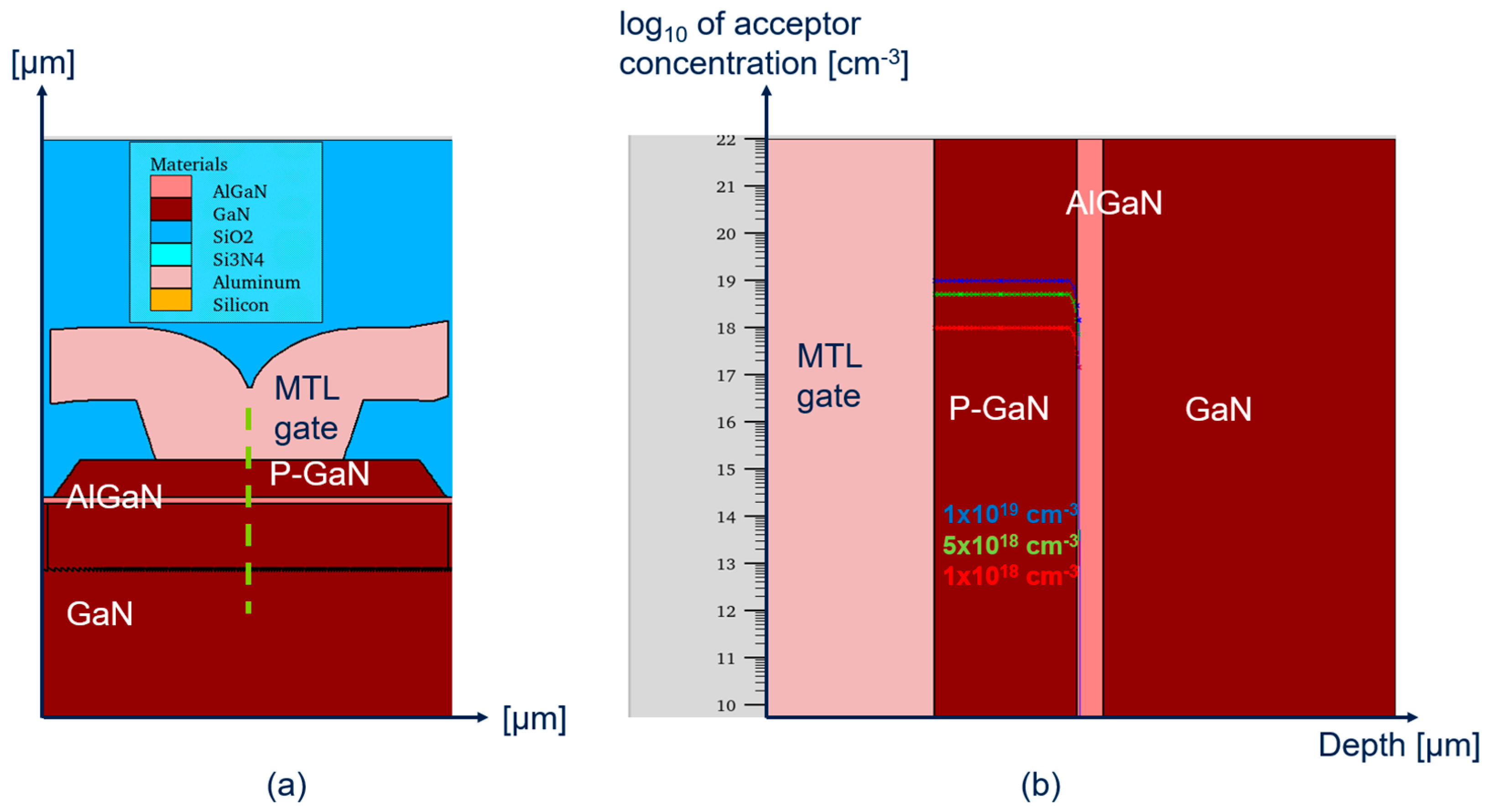
  • In the first DoE, the structure has been simulated with different levels of Mg concentration. All the Mg profiles shared no Mg out-diffusion in the AlGaN barrier, as shown in Figure 3.
The simulation results are summarized and shown in Figure 4, where it can be observed that no differences in terms of VPO have been obtained with the levels of Mg equal or above 1018 cm−3, while the pinch-off voltage has been found to be lower in the case of no acceptor concentration in the GaN cap. The explanation of this behavior can be found in the band diagrams of the gate stack (Figure 4): as long as the acceptor concentration in p-GaN is high enough to induce a depletion region whose width is shorter than the whole p-GaN height, no variations are produced in the conduction band (CB) edge close to the AlGaN/GaN heterointerface (meaning that the potential well, and so the 2DEG density, is not altered). Only when the acceptor concentration is very low (or not present at all), the extension of the depletion width can approximate the total p-GaN height, thus inducing a pull-down of the conduction band edge, which then approaches the quasi-Fermi level (EF), resulting in an early turn-on of the device (in terms of a reduced VPO).
2.
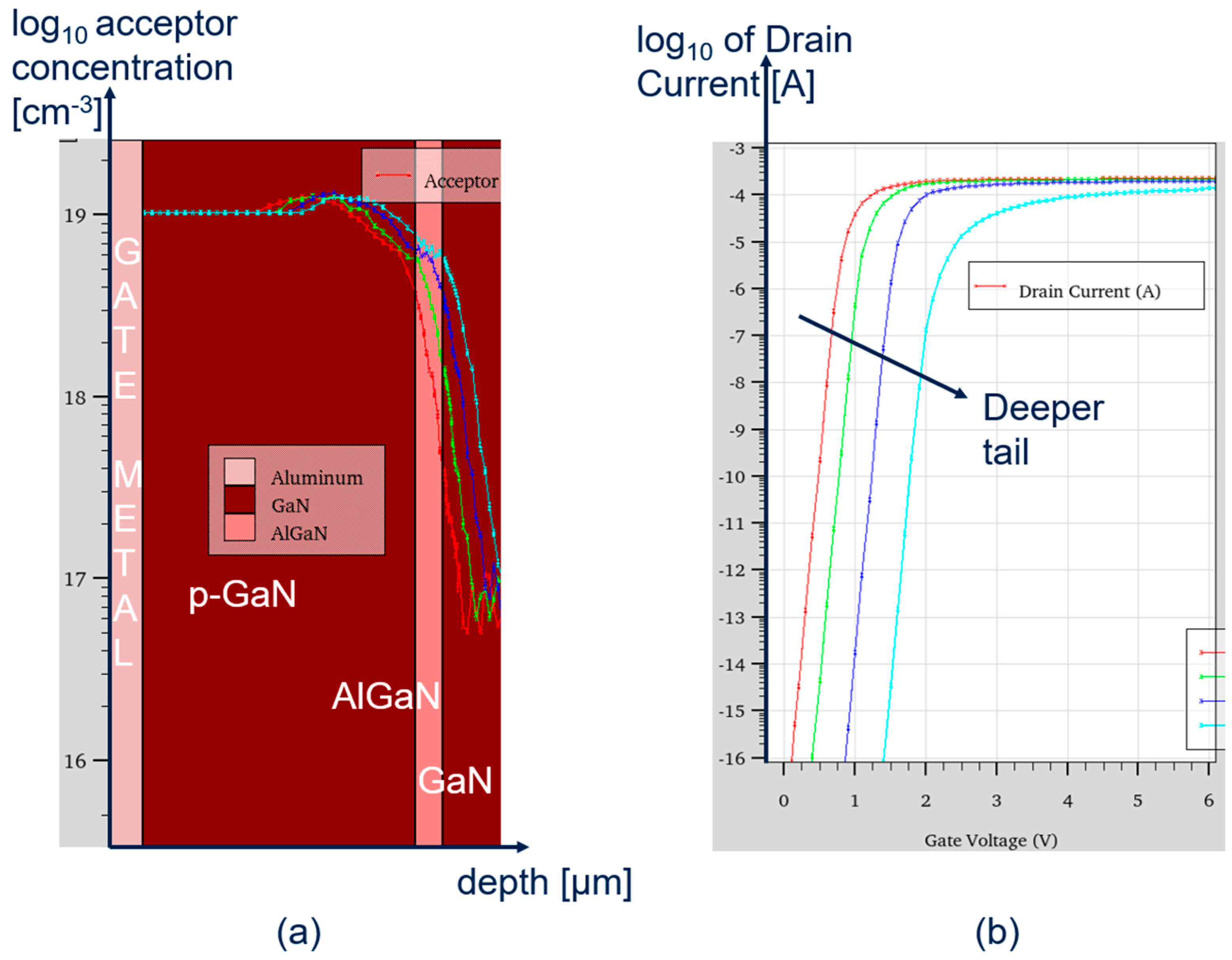
A second DoE has been performed by fixing the value of the acceptor concentration in p-GaN and comparing the different out-diffusion profiles in the AlGaN/GaN region: the different profiles have been simulated starting from an experimental out-diffusion shape (Figure 5 (a), red line) and then simply shifting the profile “tail” deeper into the AlGaN/GaN region. The results are shown in Figure 5, where it is clearly visible how the out-diffusion can influence both the pinch-off and threshold voltage. This is because the out-diffused acceptor concentration further counteracts the 2DEG density formation, thus increasing VPO (this effect has been also reported in the literature [14,21]).

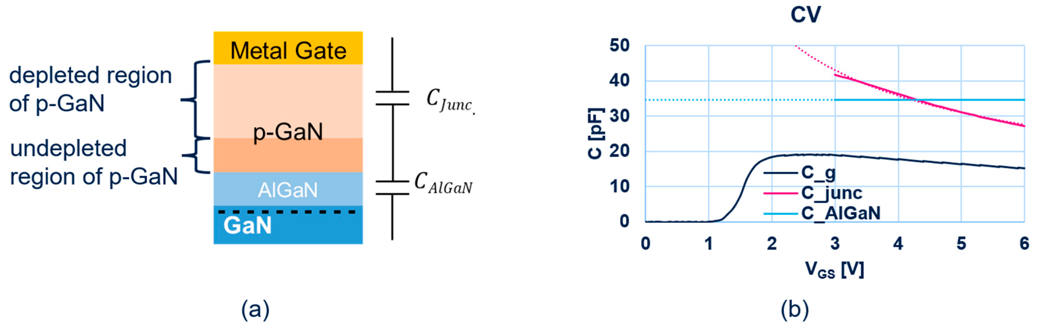
2.2. Analysis of CV Measurements

The experimental measurement of the gate capacitance can be very useful for the analysis of the device behavior since it easily allows us to extract information regarding the net acceptor concentration in p-GaN [22]. Another possible method consists of analyzing the gate leakage current but, in this latter case, information on the acceptor concentration and on the Schottky (gate metal/p-GaN) barrier can be easily extracted only if the overall gate leakage current is dominated by a bulk conduction in p-GaN and if the gate current model has been clearly identified as, e.g., a thermionic (or a thermionic-field) emission [23,24]. The measured gate capacitance curve can always be effectively analyzed using the same model, regardless of the gate current conduction mechanism (in the only assumption of the reduced gate leakage). Therefore, it is not only easier but also more reliable to obtain information on the p-GaN acceptor concentration from CV rather than from the gate current measurements. The double diode junction model of the gate stack can be exploited to understand the different capacitive contributions to the overall gate capacitance [25]. In particular, when the 2DEG channel under the p-GaN is formed (i.e., in the super-threshold region), the total gate capacitance consists of the series of the AlGaN capacitance (which can be assumed as constant) and the Schottky junction capacitance (Figure 6).
Given the expanded expression of the normalized junction capacitance:
C j = q · ϵ G a N · N A 2 · ( V b i + V M S )
the net acceptor concentration can be extracted from the gate capacitance measurements as:
N A 2 q · ϵ G a N · d d V G S ( 1 C j ) 2
Therefore, it can be observed that the acceptor concentration is the main factor modulating the gate capacitance and, if it is lowered, the gate capacitance decreases as well. In particular, under the hypothesis of very low (or absent) active Mg in p-GaN (meaning very low or zero acceptor concentrations), the measured capacitance value would be low and constant with the gate voltage, thus reducing to a dielectric-like behavior. In this work, all the shown CV measurements have been performed at a frequency of 1 MHz with an AC signal of about 20 mV after completing the measurement setup (e.g., open correction).

2.3. Different GaN Cap Processings

Three main process solutions have been implemented for better understanding the role of Mg doping and its activation as an acceptor:
  • reference process, where no intentional magnesium doping has been introduced in the GaN cap;
  • single-RTP process, characterized by an intentional Mg doping (ranging from 0.5 × 1019 cm−3 to 2 × 1019 cm−3) during the epitaxial growth of the GaN cap and a standard Rapid Thermal Processing (RTP) for Mg activation (temperature in the range of 700–850 °C for a time duration of 1–10 min), performed after the p-GaN growth;
  • multiple-RTP process, featuring intentional Mg doping during the epitaxial growth of the GaN cap and an improved RTP for Mg activation (similar conditions as in the single-RTP process, but the activation process is performed several times during the device process flow).
The differences in terms of device behavior between the undoped GaN cap and the p-doped ones have been detailed in the next section, where the effect of an improved activation process for the p-GaN (namely, the multiple-RTP process) has been thoroughly analyzed.

3. Results and Discussion

3.1. Comparison between Undoped and p-Doped GaN Cap Layer
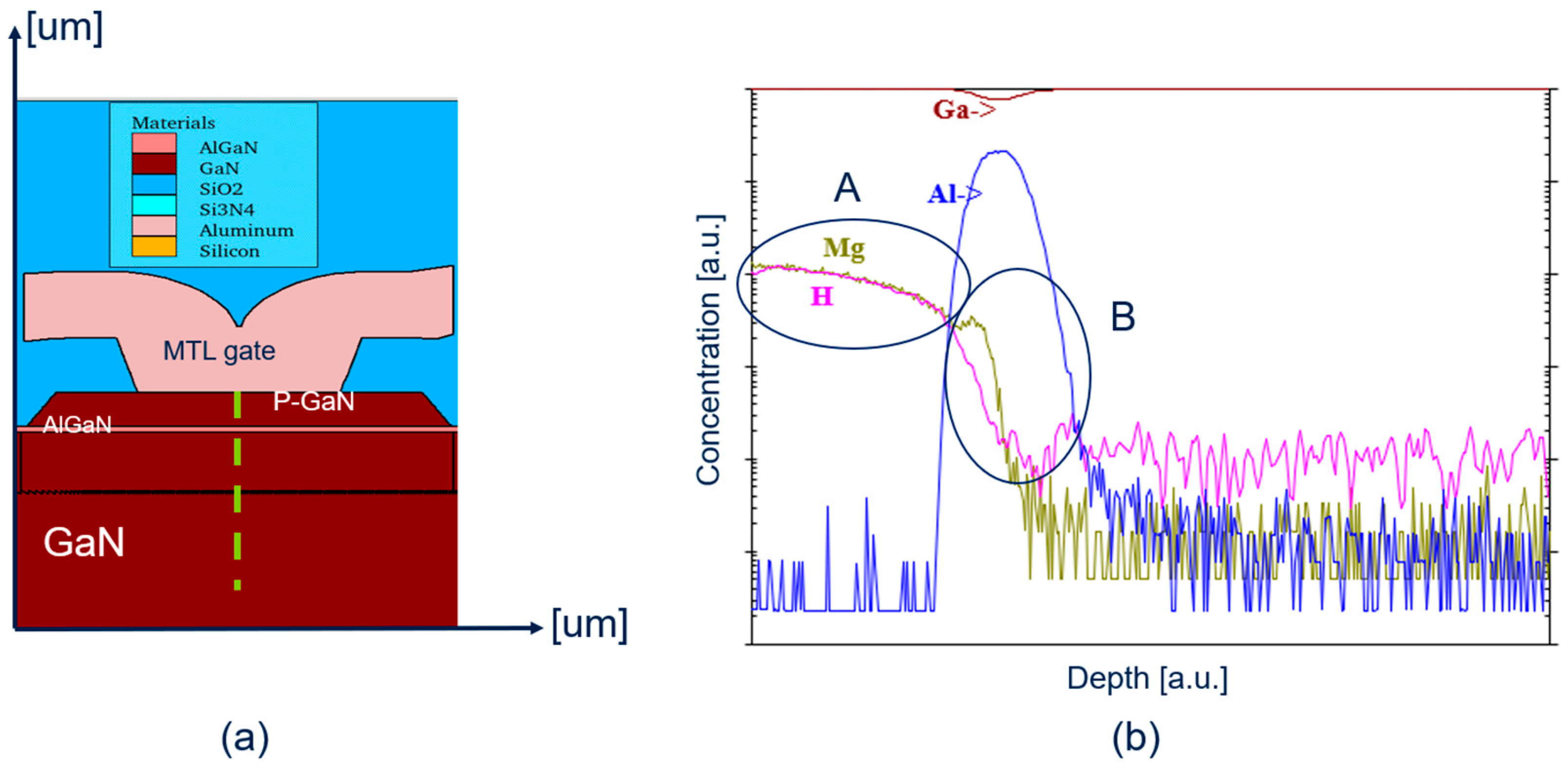
Reference process and single-RTP process devices have been characterized via DC and AC measurements. Devices with an undoped GaN cap have shown a typical depletion-mode behavior, with negative VPO and flat C/V curves. On the other hand, single-RTP process devices behave as normally-off HEMTs, showing a higher VPO (close to zero). However, the measured C/V curves of the single-RTP process exhibit the same flat behavior already observed in the reference process (Figure 7). Moreover, the gate leakage measurements have shown very similar values between the reference process and the single-RTP process.
As discussed in the previous section, a flat gate capacitance is an indication of a fully-depleted GaN cap layer, suggesting a zero or very low active Mg concentration in p-GaN (<5 × 1017 cm−3). This finding is trivially explained for the reference process (where there is no intentional Mg doping) but it is less expected for the single-RTP process. Moreover, it must be pointed out that even if the gate capacitance is flat on both processes, VPO are actually quite different. In order to deeper investigate the results observed in single-RTP process devices, Secondary-Ion Mass Spectrometry (SIMS) analyses have been performed in the shallow portion of the dedicated p-GaN capped structures. In fact, through SIMS inspection, it is possible to obtain information about the position and the concentration of the chemical species inside the structure. Figure 8 displays the structure used in the simulation and the results of the SIMS analysis performed on single-RTP process devices. As can be seen, hydrogen species was also detected, due to some contamination coming from the precursors used in the reaction chamber for the p-GaN growth.
Two different regions can be identified based on the obtained SIMS profiles and on the corresponding levels of both hydrogen and magnesium:
A.
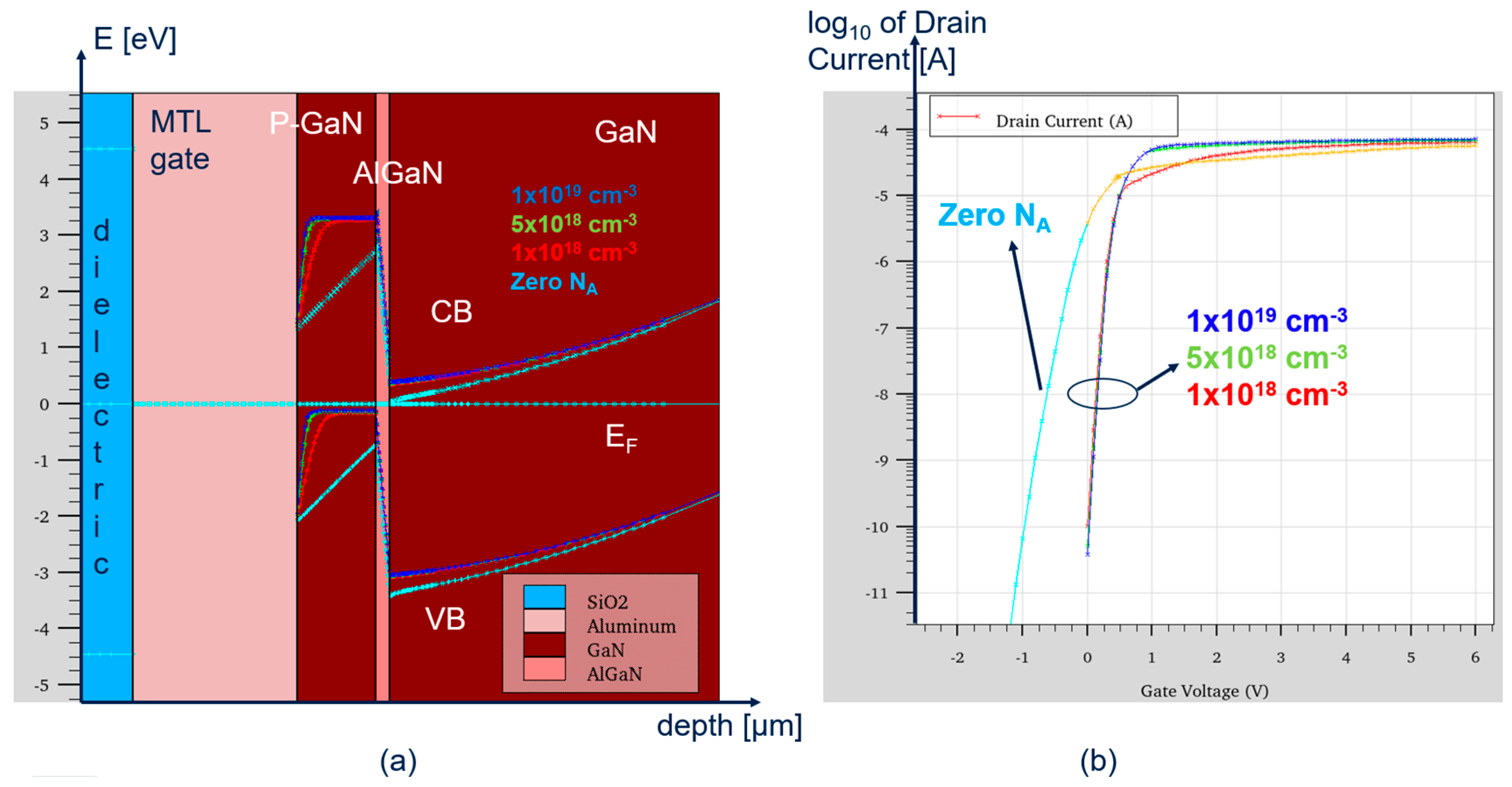
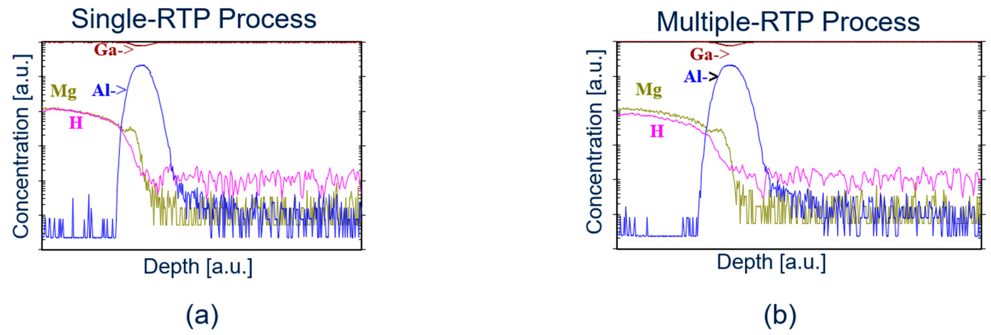
in the first region, coincident with the full p-GaN dimension, the Mg concentration is at the same level of the hydrogen (H) concentration. As reported in the literature, Mg and H can form a bond (Mg–H complexes), preventing Mg to act as an acceptor [26]. Therefore, the flatness of the CV measurement can be well explained by the very low active Mg induced by high H levels in p-GaN;
B.
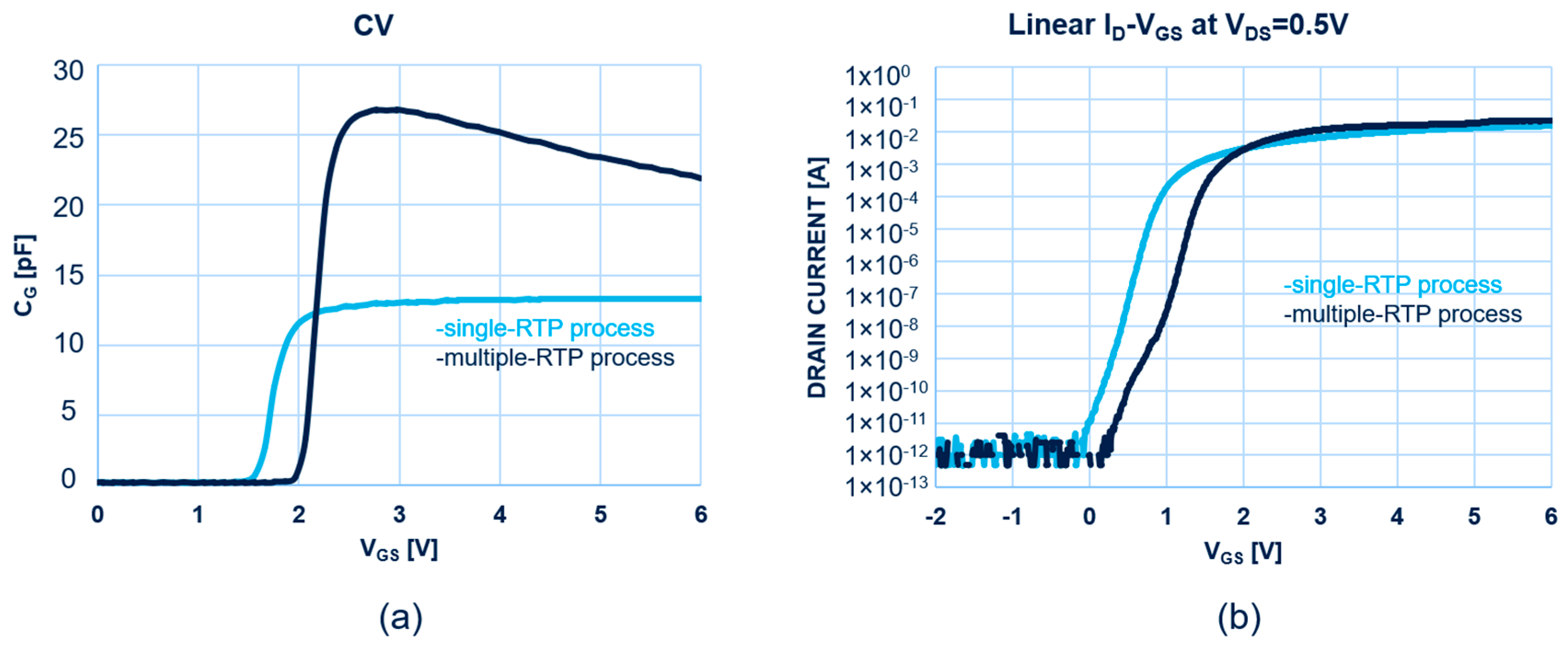
the second region, corresponding to the AlGaN barrier position, shows a difference between Mg and H concentrations, where Mg is consistently higher than H, suggesting a non-zero Mg-induced acceptor concentration close to the AlGaN barrier. This finding, as studied in the previous section, can justify a positive shift of VPO with respect to a fully undoped GaN cap (reference process), as observed in both the CV and IV measurements (Figure 7).
Therefore, the effect of Mg out-diffusion in AlGaN on VPO has been experimentally confirmed also in the case of a non-optimized p-GaN activation process, namely the single-RTP process.

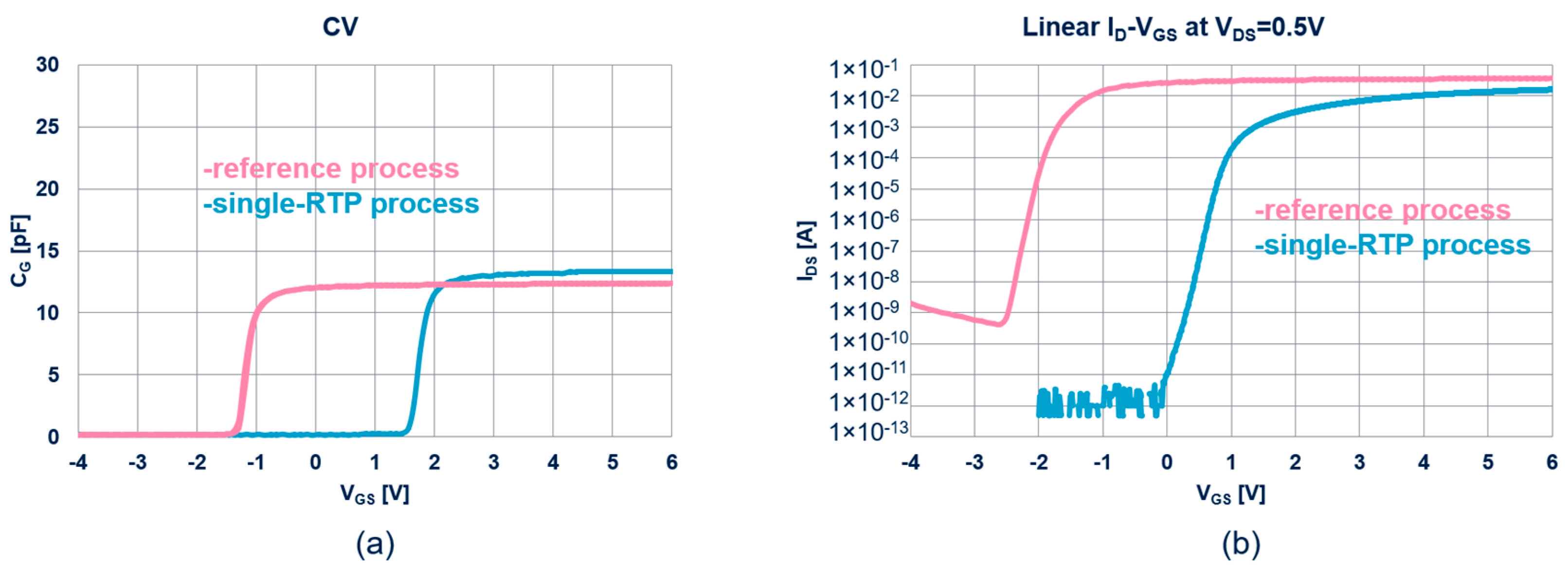
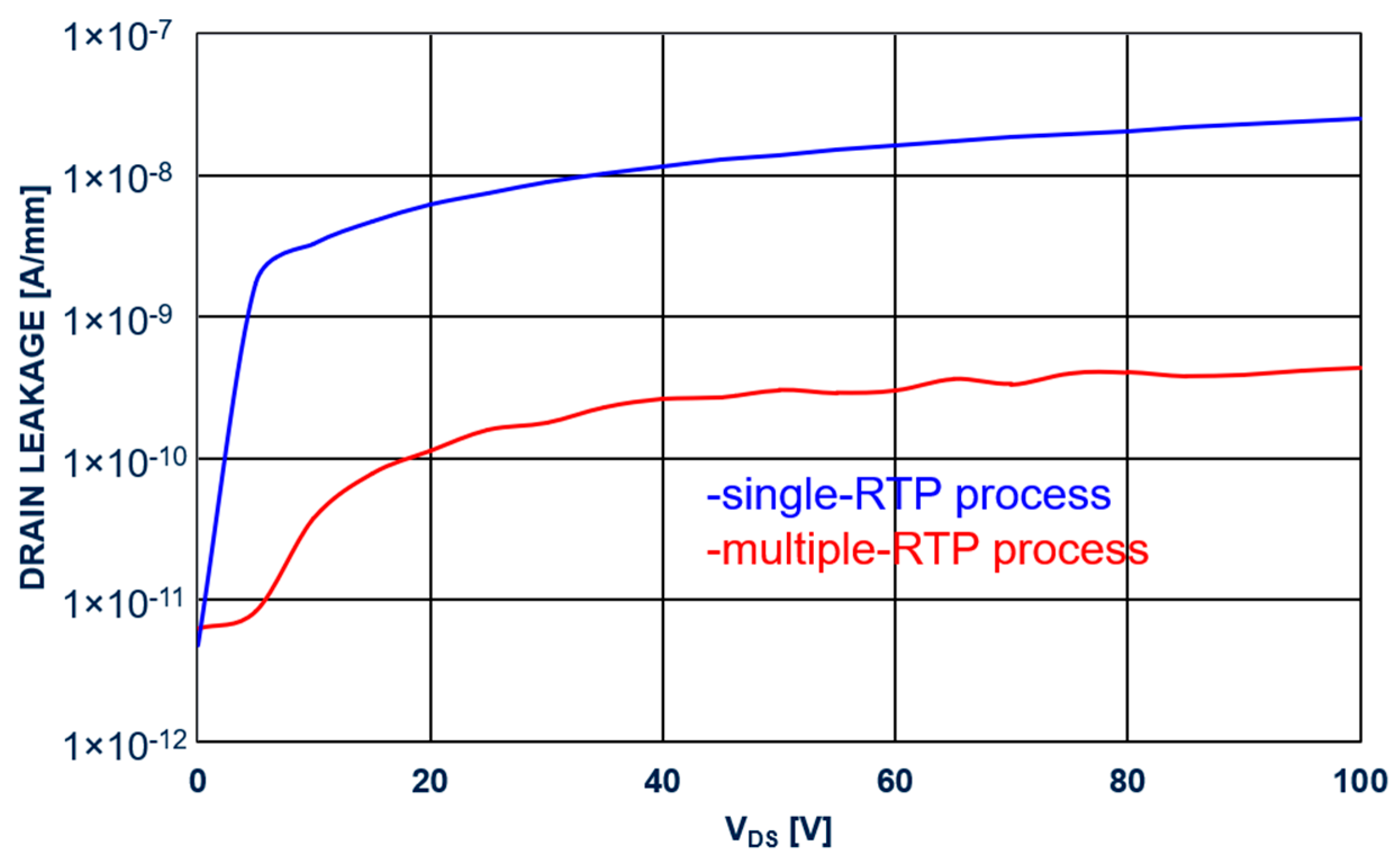
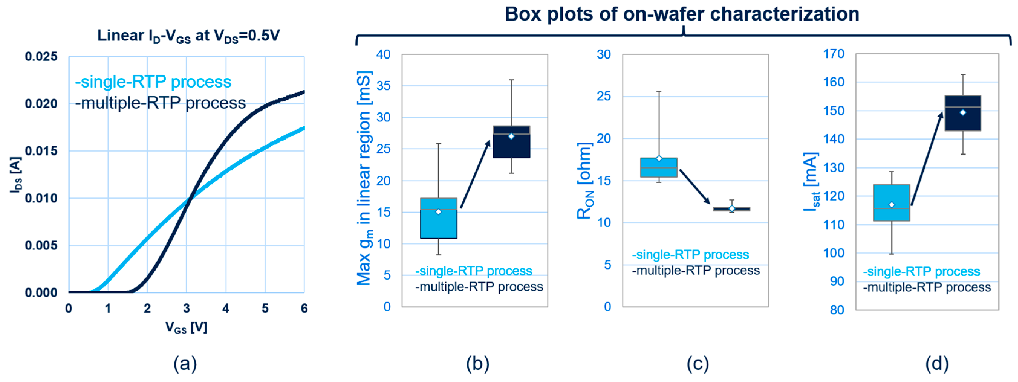
3.2. Comparison between Standard and Improved RTP

Multiple-RTP process devices have been analyzed in this sub-section. These devices share the same nominal Mg doping as the single-RTP process, but an optimized thermal treatment (RTP) has been applied for improving the activation in p-GaN. SIMS analyses have been performed also on multiple-RTP process structures and the results are shown in Figure 9: in this case, the measured H concentration is lower than Mg even along the p-GaN region, suggesting that a portion of the Mg could contribute to increasing the net acceptor concentration.
As a matter of fact, CV measurements confirm the expected non-flat behavior (typical of a Schottky junction) after the threshold and IV measurements on multiple-RTP process devices have shown an increased value of VPO with respect to the single-RTP process ones (Figure 10). This is consistent with a pulling-up of the band diagram (already described in the previous section), which is induced by the improved Mg activation in p-GaN. In this case, the extracted net acceptor concentration was about 2 × 1018 cm−3.
The higher pinch-off voltage also allows us to obtain a lower and more stable drain leakage current up to the high drain voltages (as shown in Figure 11).
Apart from the improved off-state behavior, the multiple-RTP process has also shown several advantages for the on-state operation of the device in terms of the transconductance (gm), on-resistance (RON), and saturation current (ISAT). In particular, the improved gm value has been obtained thanks to the increased gate capacitance value, given the fact the transconductance is not only dependent on the mobility but also on the gate capacitance [27]. Moreover, the RON intra-wafer spread has been highly reduced, as shown in Figure 12, given the insensitivity to the gate metal work-function for the higher levels of Mg activation [14].
On the improved devices (multiple-RTP process), a complete temperature characterization of the parameters reported before has been performed. The results of this characterization have been summarized in the graphs below (Figure 13), where all the parameters have been normalized with respect to their room temperature value.

4. Conclusions

A comparison between AlGaN/GaN HEMTs with undoped and p-doped GaN gate modules has been investigated in this work. TCAD simulations have been carried out to study the effect of the net acceptor concentration (present in the gate stack) on the band diagram of the structure and therefore on the pinch-off voltage of the transistor. Experimental results on three different processes have underlined the relevance of an improved annealing process for the p-GaN gate. In particular, the results obtained on multiple-RTP process devices (the ones characterized by an improved RTP) have been analyzed in detail, showing increased VPO values, more stable off-state performances (at a zero-gate voltage) in terms of a reduced drain leakage, and better on-state behavior (consisting of reduced on-resistances and enhanced saturation currents).
As a result of the previously commented theoretical study and experimental results, some general considerations can be drawn to summarize the effect of the different Mg activation levels on the VPO:
  • whether the active Mg concentration in p-GaN is high or low, there can be an indirect influence of the Mg doping level on the VPO via its out-diffusion in the AlGaN barrier;
  • if the active Mg concentration in p-GaN is rather low, the depletion width of the Schottky junction can cover the whole p-GaN dimension, reaching the AlGaN barrier, and thus pull down the entire band diagram (VPO lowering);
  • if the active Mg concentration in p-GaN is high enough to induce a depletion width shorter than the full p-GaN height, there will be no direct dependence of VPO on the Mg doping level nor on the Schottky barrier height.
Apart from the above-mentioned advantages, it should be taken into consideration that an improvement in the magnesium activation can also produce some of the following drawbacks:
  • Higher gate leakage [23];
  • Higher hysteresis and VTH instability [28];
  • Increased current collapse in dynamic conditions [21].
These issues should be addressed as well while optimizing the activation process, e.g., limiting their impact on the device behavior by implementing additional solutions (improved passivation, pre-passivation cleaning treatments, etc.). Therefore, future studies will focus on the optimization of the entire p-GaN/AlGaN/GaN heterostructure, in order to limit the gate leakage and improve the dynamic performances in the soft- and hard-switching modes, considering also the different thicknesses of the passivation layer and compounds. Another aspect to be explored is the refinement of the p-GaN growth conditions, e.g., in terms of pressure and temperature, which play an important role in the improvement of the gate stack. However, this study already provides a detailed understanding of the important effect of Mg activation and can be used as a further step in the optimization of p-GaN HEMTs, both in off-condition as well as in on-state.

Author Contributions

Methodology, G.G. (Giuseppe Greco) and M.M.; Investigation, C.M.; Writing—original draft, G.G. (Giovanni Giorgino); Supervision, M.E.C., C.T., P.F., F.R. and F.I. All authors have read and agreed to the published version of the manuscript.

Funding

This work has been carried out in the framework of the European Project GaN4AP (Gallium Nitride for Advanced Power Applications). The project has received funding from the Electronic Component Systems for European Leadership Joint Undertaking (ECSEL JU) under Grant Agreement No. 101007310. This Joint Undertaking receives support from the European Union’s Horizon 2020 Research and Innovation Programme, and Italy, Germany, France, Poland, Czech Republic, and the Netherlands.

Data Availability Statement

The data presented in this study are available on request from the corresponding author. The data are not publicly available due to STMicroelectronics confidentiality policies.

Acknowledgments

The authors would like to thank Gianluca Marletta, Santo Reina, and Antonino Parisi for their technical support.

Conflicts of Interest

The authors declare no conflict of interest.

References

  1. Mishra, U.K.; Parikh, P.; Wu, Y.F. AlGaN/GaN HEMTs—An Overview of Device Operation and Applications. Proc. IEEE 2002, 90, 1022–1031. [Google Scholar] [CrossRef]
  2. Mishra, U.K.; Shen, L.; Kazior, T.E.; Wu, Y.F. GaN-Based RF Power Devices and Amplifiers. Proc. IEEE 2008, 96, 287–305. [Google Scholar] [CrossRef]
  3. Meneghini, M.; Tajalli, A.; Moens, P.; Banerjee, A.; Zanoni, E.; Meneghesso, G. Trapping phenomena and degradation mechanisms in GaN-based power HEMTs. Mater. Sci. Semicond. Process. 2018, 78, 118–126. [Google Scholar] [CrossRef]
  4. Ambacher, O.; Foutz, B.; Smart, J.; Shealy, J.R.; Weimann, N.G.; Chu, K.; Murphy, M.; Sierakowski, A.J.; Schaff, W.J.; Eastman, L.F.; et al. Two dimensional electron gases induced by spontaneous and piezoelectric polarization in undoped and doped AlGaN/GaN heterostructures. J. Appl. Phys. 2000, 87, 334–344. [Google Scholar] [CrossRef]
  5. Ambacher, O.; Smart, J.; Shealy, J.R.; Weimann, N.G.; Chu, K.; Murphy, M.; Schaff, W.J.; Eastman, L.F.; Dimitrov, R.; Wittmer, L.; et al. Two-dimensional electron gases induced by spontaneous and piezoelectric polarization charges in N- and Ga-face AlGaN/GaN heterostructures. J. Appl. Phys. 1999, 85, 3222–3233. [Google Scholar] [CrossRef]
  6. Meneghini, M.; De Santi, C.; Abid, I.; Buffolo, M.; Cioni, M.; Khadar, R.A.; Nela, L.; Zagni, N.; Chini, A.; Medjdoub, F.; et al. GaN-based power devices: Physics, reliability, and perspectives. J. Appl. Phys. 2021, 130, 181101. [Google Scholar] [CrossRef]
  7. Roccaforte, F.; Greco, G.; Fiorenza, P.; Iucolano, F. An Overview of Normally-Off GaN-Based High Electron Mobility Transistors. Materials 2019, 12, 1599. [Google Scholar] [CrossRef] [PubMed]
  8. Greco, G.; Iucolano, F.; Roccaforte, F. Review of technology for normally-off HEMTs with p-GaN gate. Mater. Sci. Semicond. Process. 2018, 78, 96–106. [Google Scholar] [CrossRef]
  9. Uemoto, Y.; Hikita, M.; Ueno, H.; Matsuo, H.; Ishida, H.; Yanagihara, M.; Ueda, T.; Tanaka, T.; Ueda, D. Gate injection transistor (GIT)—A normally-off AlGaN/GaN power transistor using conductivity modulation. IEEE Trans. Electron Devices 2007, 54, 3393–3399. [Google Scholar] [CrossRef]
  10. Kumar, A.; Berg, M.; Wang, Q.; Salter, M.; Ramvall, P. Growth of p-type GaN—The role of oxygen in activation of Mg-doping. Power Electron. Devices Compon. 2023, 5, 100036. [Google Scholar] [CrossRef]
  11. SILVACO. ATLAS User’ s Manual (Device Simulation Software); SILVACO: Santa Clara, CA, USA, 2019. [Google Scholar]
  12. Iucolano, F.; Greco, G.; Roccaforte, F. Correlation between microstructure and temperature dependent electrical behavior of annealed Ti/Al/Ni/Au Ohmic contacts to AlGaN/GaN heterostructures. Appl. Phys. Lett. 2013, 103, 201604. [Google Scholar] [CrossRef]
  13. Greco, G.; Fiorenza, P.; Giannazzo, F.; Bongiorno, C.; Moschetti, M.; Bottari, C.; Alessandrino, M.S.; Iucolano, F.; Roccaforte, F. Threshold voltage instability by charge trapping effects in the gate region of p-GaN HEMTs. Appl. Phys. Lett. 2022, 121, 233506. [Google Scholar] [CrossRef]
  14. Bakeroot, B.; Stockman, A.; Posthuma, N.; Stoffels, S.; Decoutere, S. Analytical Model for the Threshold Voltage of p-(Al)GaN High-Electron-Mobility Transistors. IEEE Trans. Electron Devices 2018, 65, 79–86. [Google Scholar] [CrossRef]
  15. Garcia, F.; Shamsir, S.; Islam, S.K. A compact model and TCAD simulation for GaN-gate injection transistor (GIT). Solid-State Electron. 2019, 151, 52–59. [Google Scholar] [CrossRef]
  16. SILVACO. ATHENA User’ s Manual (Process Simulation Software); SILVACO: Santa Clara, CA, USA, 2015. [Google Scholar]
  17. Farahmand, M.; Garetto, C.; Bellotti, E.; Brennan, K.; Goano, M.; Ghillino, E.; Ghione, G.; Albrecht, J.; Ruden, P. Monte Carlo simulation of electron transport in the III-nitride wurtzite phase materials system: Binaries and ternaries. IEEE Trans. Electron Devices 2001, 48, 535–542. [Google Scholar] [CrossRef]
  18. Kakanakova-Georgieva, A.; Papamichail, A.; Stanishev, V.; Darakchieva, V. Incorporation of Magnesium into GaN Regulated by Intentionally Large Amounts of Hydrogen during Growth by MOCVD. Phys. Status Solidi (b) 2022, 259, 2200137. [Google Scholar] [CrossRef]
  19. Jaud, M.-A.; Baines, Y.; Charles, M.; Morvan, E.; Scheiblin, P.; Torres, A.; Plissonnier, M.; Barbe, J.-C. TCAD for gate stack optimization in pGaN Gate HEMT devices. In Proceedings of the 2017 International Conference on Simulation of Semiconductor Processes and Devices (SISPAD), Kamakura, Japan, 7–9 September 2017; pp. 205–208. [Google Scholar]
  20. Liou, J.J.; Ortiz-Conde, A.; Garcia-Sanchez, F. Analysis and Design of MOSFETs: Modeling, Simulation and Parameter Extraction; Kluwer Academic Publishers: New York, NY, USA, 1998. [Google Scholar]
  21. Posthuma, N.E.; You, S.; Liang, H.; Ronchi, N.; Kang, X.; Wellekens, D.; Saripalli, Y.N.; Decoutere, S. Impact of Mg out-diffusion and activation on the p-GaN gate HEMT device performance. In Proceedings of the 2016 28th International Symposium on Power Semiconductor Devices and ICs (ISPSD), Prague, Czech Republic, 12–16 June 2016. [Google Scholar]
  22. Hilibrand, J.; Gold, R.D. Determination of the Impurity Distribution in Junction Diodes From Capacitance-Voltage Measurements. RCA Rev. 1960, 21, 245. [Google Scholar]
  23. Padovani, F.; Stratton, R. Field and thermionic-field emission in Schottky barriers. Solid-State Electron. 1966, 9, 695–707. [Google Scholar] [CrossRef]
  24. Greco, G.; Iucolano, F.; Di Franco, S.; Bongiorno, C.; Patti, A.; Roccaforte, F. Effects of Annealing Treatments on the Properties of Al/Ti/p-GaN Interfaces for Normally OFF p-GaN HEMTs. IEEE Trans. Electron Devices 2016, 63, 2735–2741. [Google Scholar] [CrossRef]
  25. Modolo, N.; Tang, S.W.; Jiang, H.J.; De Santi, C.; Meneghini, M.; Wu, T.L. A Novel Physics-Based Approach to Analyze and Model E-Mode p-GaN Power HEMTs. IEEE Trans. Electron Devices 2021, 68, 1489–1494. [Google Scholar] [CrossRef]
  26. Youn, D.-H.; Lachab, M.; Hao, M.; Sugahara, T.; Takenaka, H.; Naoi, Y.; Sakai, S. Investigation on the P-Type Activation Mechanism in Mg-doped GaN Films Grown by Metalorganic Chemical Vapor Deposition. Jpn. J. Appl. Phys. 1999, 38, 631–634. [Google Scholar] [CrossRef]
  27. Chen, K.J.; Häberlen, O.; Lidow, A.; lin Tsai, C.; Ueda, T.; Uemoto, Y.; Wu, Y. GaN-on-Si Power Technology: Devices and Applications. IEEE Trans. Electron Devices 2017, 64, 779–795. [Google Scholar] [CrossRef]
  28. Tallarico, A.N.; Stoffels, S.; Posthuma, N.; Decoutere, S.; Sangiorgi, E.; Fiegna, C. Threshold Voltage Instability in GaN HEMTs with p-type Gate: Mg Doping Compensation. IEEE Electron Device Lett. 2019, 40, 518–521. [Google Scholar] [CrossRef]
Figure 1. Typical simplified structure of a p-GaN HEMT (DUT). Normally-off operation is obtained by means of a p-GaN layer epitaxially grown on top of the AlGaN Barrier. A proper design of the AlGaN thickness and Al% is used to modulate the two-dimensional electron gas (2DEG) density at the AlGaN/GaN interface.
Crystals 13 01309 g001
Figure 2. Linear transcharacteristic (IDS-VGS) of the DUT in semi-log scale. The pinch−off voltage is extracted as the VGS value of the curve corresponding to a chosen low IDS level (green horizontal dashed line).
Crystals 13 01309 g002
Figure 3. (a) Cross−ection of the DUT emulated via the TCAD simulator; (b) comparison between three different acceptor concentrations in p-GaN (DoE on Mg doping), evaluated on a cutline of (a), determined by the vertical dashed line.
Crystals 13 01309 g003
Figure 4. (a) Band diagrams of the gate stack at zero gate bias for different acceptor concentrations; (b) comparison between the corresponding IDS−VGS in semi−log scale (W = 0.4 mm).
Crystals 13 01309 g004
Figure 5. (a) Comparison between four different acceptor out-diffusion profiles in p−GaN; (b) the related comparison between the corresponding IDS−VGS in semi−log scale (W = 0.4 mm).
Crystals 13 01309 g005
Figure 6. (a) Schematic cross-section of the gate stack of the DUT, in which the total gate capacitance is the series of the junction capacitance and the AlGaN capacitance (1/CG = 1/CJuncc + 1/CAlGaN); (b) an example of the different CV curves obtained starting from the gate capacitance measurements (total gate area = 0.00016 cm2). Solid lines show the total gate capacitance (C_g), the Schottky junction capacitance (C_junc), and the AlGaN capacitance (C_AlGaN), while the dashed lines indicate the ideal continuation of these last two capacitances before the 2DEG formation under the p-GaN.
Crystals 13 01309 g006
Figure 7. (a) Comparison between gate capacitance measurements of reference process and single−RTP process is depicted; (b) the linear transcharacteristics of reference process and single−RTP process are reported in semi−log scale.
Crystals 13 01309 g007
Figure 8. (a) Highlight of the region inspected via SIMS; (b) shallow SIMS profiles for magnesium, hydrogen, aluminum, and gallium species evaluated on a cutline of (a), determined by the green vertical dashed line: two different regions, A and B, can be identified.
Crystals 13 01309 g008
Figure 9. Comparison between shallow SIMS profiles of (a) single-RTP process and (b) multiple-RTP process.
Crystals 13 01309 g009
Figure 10. (a) Comparison between gate capacitance measured on single−RTP process and multiple−RTP process; (b) the linear ID−VGS of single−RTP process and multiple−RTP process are displayed in semi−log scale.
Crystals 13 01309 g010
Figure 11. Drain leakage measurements at VG = 0 V for single-RTP process and multiple-RTP devices (median values of the measurements on nine on-wafer devices are reported).
Crystals 13 01309 g011
Figure 12. (a) Comparison between the linear ID-VGS of single-RTP process and multiple-RTP process devices, (b) the maximum conductance in linear region (max gm), (c) the on-resistance (RON), and (d) the saturation current (ISAT) are reported and compared between the two process solutions for a device with a total gate width of 0.4 mm.
Crystals 13 01309 g012
Figure 13. The temperature dependence of (a) the maximum conductance in linear region (max gm), (b) the on−resistance (RON), and (c) the saturation current (ISAT) is displayed for multiple−RTP process devices (total gate width of 0.4 mm, median values on nine samples).
Crystals 13 01309 g013
Disclaimer/Publisher’s Note: The statements, opinions and data contained in all publications are solely those of the individual author(s) and contributor(s) and not of MDPI and/or the editor(s). MDPI and/or the editor(s) disclaim responsibility for any injury to people or property resulting from any ideas, methods, instructions or products referred to in the content.

