Article

Aluminum Phosphide van der Waals Bilayers with Tunable Optoelectronic Properties under Biaxial Strain

1
Hubei Key Laboratory of Radiation Chemistry and Functional Materials, Hubei University of Science and Technology, Xianning 437100, China
2
School of Nuclear Technology and Chemistry & Biology, Hubei University of Science and Technology, Xianning 437100, China
3
School of Science, Hubei University of Automotive Technology, Shiyan 442002, China
*
Authors to whom correspondence should be addressed.
These authors contributed equally to this work.
Crystals 2023, 13(4), 597; https://doi.org/10.3390/cryst13040597
Submission received: 19 February 2023 / Revised: 17 March 2023 / Accepted: 28 March 2023 / Published: 1 April 2023
(This article belongs to the Special Issue 2D Crystalline Nanomaterials)

Abstract

:
The electronic and optical properties of three types of aluminum phosphide bilayers are examined using density functional theory. The results indicate that they all possess proper direct gaps, which exhibit a rich variety of behaviors depending on the strain. The band gaps of these aluminum phosphide bilayers could be easily tuned in the energy range from 0 eV to 1.9 eV under a wide range of biaxial strain. Additionally, band gap transitions between direct and indirect types are found when the external strain applied on them is changed from −12% to 12%. In addition, it was found that these AlP bilayers show strong light-harvesting ability for the ultraviolet light range of the solar spectrum (400–100 nm). The results obtained here indicate that these aluminum phosphide bilayers may have significant potential applications in future nanoelectric fields.

1. Introduction

Graphene is the first example of two-dimensional (2D) single-layer material, which has opened a new window to nanostructure materials [1,2]. From graphene, a large number of new two-dimensional materials have been synthesized, and the new two-dimensional material family is becoming increasingly large and prosperous. Owing to the electron confinement effect and the absence of interlayer interaction, 2D materials usually differ significantly from their bulk counterparts [3,4,5]. They also have completely different novel properties, such as electronic structure, optical properties and mechanical properties. The unique combination of excellent physical and chemical properties of 2D materials has aroused enormous attention, and many freestanding monolayer crystals, such as hexagonal BN, transition metal dichalcogenides, antimonene, etc., were systematically studied, leading to various applications [6,7,8]. The design and development of nanodevices based on new 2D materials promote the rapid development of nanoelectronic technology. It is important for people to design and synthesize novel 2D crystals, and further explore new applications in future nanoelectronic fields.
Aluminum phosphide (AlP) is a typical III–V semiconductor with a proper band gap [9]. In the periodic table, it is in the row next to boron nitride; however, there is relatively little research on it. Its bulk form has many excellent optoelectronic properties and shows magnetic properties after doping of Cr or Ga atoms [9,10]. It has been used to manufacture nanostructure devices, for example, detectors, diodes, spintronics, etc. [10,11,12]. Novel electronic and magnetic properties of AlP are induced through doping. Therefore, it is also a promising material for new nanoelectric devices [13,14,15]. As the isoelectronic counterpart of silicone, low-dimensional AlP materials have attracted the interest of many researchers [16,17,18,19]. For example, Tong et al. theoretically and firstly described two 2D single-layer structures of AlP structures (T-structure AlP and V-structure AlP) and their common electronic properties [17]. Hu et al. deeply studied the geometric configurations and electronic properties of V-structure AlP (V-AlP) using first-principles calculation [19]. It is reported that external strain and layer stacking can both be used to modify the geometric configurations as well as the optoelectronic property of the V-AlP monolayer. The V-AlP monolayer belongs to the space group Pmn21 and from the top view it has inequilateral hexagonal rings. In a vertical orientation, it resembles a large buckle. The T-AlP monolayer belongs to the space group P4/nmm and it has a layered structure. The V-AlP monolayer has been found to be stronger than the T-AlP monolayer [18,19]. These AlP monolayers are new 2D semiconductor materials with wide potential application prospects in the near future. As new 2D materials, their properties can be regulated through a variety of physical means, such as doping, defect engineering, stress, electric field, van der Waals stacking and chemical modification [19]. Through van der Waals stacking, especially heterojunction stacking, new physical characteristics different from their constituent units can be induced. At the same time, they have the advantages of their constituent units. Homogeneous van der Waals stacking can also induce new properties. As a simple example, graphene multilayer and monolayer have different infrared light absorption intensities; therefore, in the field of physical therapy, single-layer graphene will be used, and the industrial field may use more than two layers of graphene [2].
As new 2D materials, AlP monolayers provide new building units for van der Waals nanostructures. In experiments, phosphorene-graphene hetero-bilayer structures have already been synthesized and they possess an intrinsic Schottky contact at the photonic crystal interface, in which the Schottky barrier can be modulated by strains and electric fields. Subsequent to this progress, it is natural to explore hetero-systems composed of T-AlP and V-AlP. Here, we perform comprehensive investigation on the structures and properties of V-AlP/V-AlP, T-AlP/T-AlP and T-AlP/V-AlP bilayers. This study offers new insights into the optoelectronic properties of AlP bilayers through strain engineering, which can be exploited in the design of new optoelectronic devices based on 2D AlP materials.

2. Methods

All the crystal structures of AlP bilayers are optimized before calculating their material properties. The calculations of the electronic properties of AlP bilayers are performed in CASTEP [20]. The Perdew–Burke–Ernzerhof functional and the Heyd–Scuseria–Ernzerhof hybrid functional are both used, and in the following they are labeled as PBE functional and HSE06 functional, respectively [21,22,23,24]. The vacuum region adopted is greater than 20Å. The van der Waals (vdW) calculation is performed based on the Tkatchenko–Scheffler approaches [25]. The basis set of valence electronic states is set to be 3s2 3p1 for Al and 3s2p3 for P, respectively. The kinetic energy cutoff for the plane–wave expansion is set to 1000 eV. The energy convergence criterion was set to 10−7 eV. All the structures were relaxed until the largest forces were less than 10−5 eV/Å. The definitions of cohesive energy and biaxial uniform strain are the same as in reference [19].

3. Results and Discussions

3.1. Structural Properties

The crystal structures of the AlP bilayer after full relaxation are shown in Figure 1. The characteristic parameters of the 2D AlP bilayers (for comparison, the parameters of two type AlP monolayer are also provided) are listed in Table 1. For abbreviation, the three types of AlP bilayers, T-AlP/V-AlP, T-AlP/T-AlP and V-AlP/V-AlP, are indicated by T/V-AlP, T-AlP and V-AlP, respectively, in the following. Stacking orders can significantly influence the energy band gap of bilayer van der Waals crystal. It is also necessary to research the influence of layer stacking order on the energy band gap of the AlP bilayers. In the AA-stacking pattern, the two AlP sheets are aligned without any rotation or displacement. For the AB-stacking pattern, the two AlP sheets shift along the lattice vector for a distance of half a cell. We optimized the bilayers of V-AlP and T-AlP in the AA and AB stacking orders. It was found that different stacking patterns cause almost no difference in structural parameters (lattice constants, bond lengths, etc). Interestingly, it was found that AA stacking of both V-AlP and T-AlP bilayers is energetically favorable for their lower total energy, which are, respectively, 16.7 meV and 11.6 meV per atom lower than those of AB-stacked layers. Therefore, in the following section, the AlP bilayer structures are formed by vertical AA stacking with weak interlayer vdW interaction [19,25].
To obtain the most stable bilayer structures of AlP, we examine the total energy of the systems with various distances between the two layers, as shown in Figure 2. It is found that the distance between the two layers of the three most stable vdW bilayer structures are 3.4 Å, 3.6 Å and 1.6 Å, respectively. The lattice constants’ mismatch of the T-AlP and V-AlP in the T/V-AlP bilayer crystal is below 1.5%, which is tolerable. The vertical distances between the two layers (distances between the two dashed lines in Figure 1) are 3.4 Å, 3.6 Å and 1.6 Å respectively, which are in consistent with the vdW interactions. In these stable vdW bilayer systems, the two layers of AlP are combined with each other via vdW interactions. To examine the kinetic stabilities of these three types of AlP bilayers, their cohesive energy values are calculated and compared.
As shown in the cohesive energy values in Table 1, it was found that all the AlP bilayers have high thermal stability, which is indicated by the negative values (the values are −4.94, −4.85 eV and −5.00 eV for the T/V-AlP, T-AlP and V-AlP bilayers, respectively) [26]. The thermal stability of V-AlP is slightly better than that of the T/V-AlP and T-AlP bilayers. The cohesive energy of the blue phosphorene monolayer is −5.18 eV, and it almost equals these AlP bilayers [27]. The thickness of the AlP monolayer and bilayers are shown and compared in Table 1. It is found that the thickness value of the T/V-AlP bilayer is between those of the T-AlP bilayer and the V-AlP bilayer, and the thickness of the V-AlP bilayer is 30% thinner than that of the T-AlP bilayer. The average bond length of the V-AlP monolayer is 0.02 Å shorter than that of the V-AlP bilayer, while the average bond length of the T-AlP monolayer is 0.16 Å longer than that of the T-AlP bilayer. Of the three AlP bilayers, the average bond length of the T/V-AlP bilayer is the longest, and the average bond length of the T-AlP bilayer is the shortest.

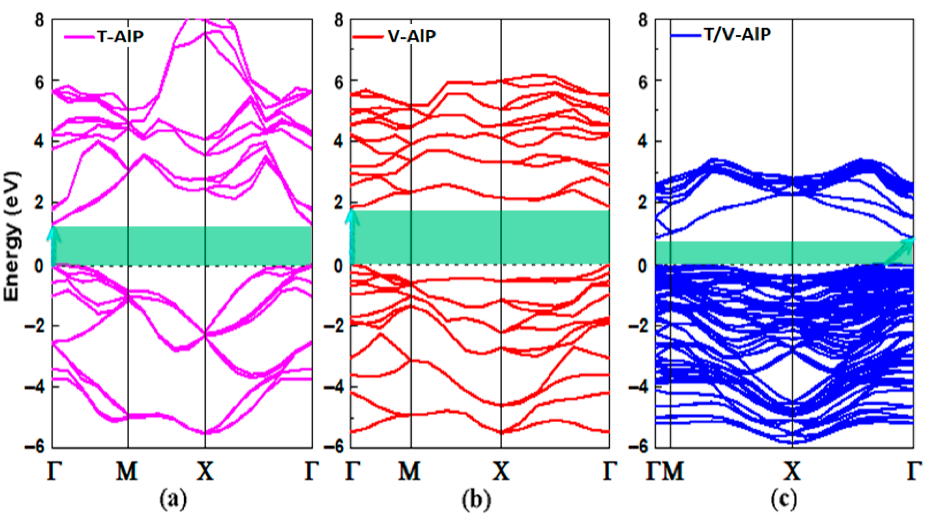
3.2. Electronic Properties

The band structures of these AlP bilayer systems are calculated in detail, as shown in Figure 3. As shown in Figure 3a,b, the direct band gaps (the cyan arrows) of 1.29 eV and 1.86 eV are obtained for the T-AlP and V-AlP bilayers, respectively. As shown in Figure 3c, the indirect band gap of 0.86 eV is obtained for the T/V-AlP bilayer. The indirect band gap characteristic of 2D material is a well-known shortcoming of their application in optoelectronic devices. Therefore, the electronic properties of T/V-AlP bilayers are to be modified by some physical method in a potential semiconductor for optoelectronic devices.
In Figure 4, the projected density of states (PDOS) of the AlP bilayers are shown. The Mulliken layout analysis of is provided in Table S1. It is found that the valence band edges for all AlP bilayers are contributed mainly by the p orbitals of P atoms. For the conduction band edge, it is determined by s orbitals of Al atoms in T-AlP bilayer (As shown in Figure 4a) and p orbitals of Al atoms in the V-AlP bilayer (As shown in Figure 4b, which also exhibit no difference from their monolayers [18,19]). In Figure 4c, it is shown that the s orbitals of Al atoms determine the conduction band edge in the T/V-AlP bilayer. The electron density difference maps of the T-AlP, V-AlP and T/V-AlP bilayers are given in Figure S1. This is in consistent with its low energy band gap compared with those of the T-AlP and V-AlP bilayers.
External in-plain strain is proved to be an effective physical method to tune the geometric configuration and common physical properties of 2D crystals [28,29]. However, the electronic property of graphene is not sensitive to external strain [30]. Hence, on one hand we are interested in exploring whether applied stress is effective in changing the geometric configurations of AlP bilayers and their electronic properties. On the other hand, we doubt whether the indirect-direct transition of energy band structure of the T-AlP bilayer can be induced by external strain. Therefore, many computations are performed on these AlP bilayers under a wide range of biaxial strain. The variations in the band gaps of T-AlP, V-AlP and T/V-AlP bilayers versus biaxial strain are plotted in Figure 5. In Figure 6, under the axial strain applied along the lattice direction from 20% to +8%, the direct band gap character of V-AlP is retained. The value of the direct band gap decreases with the increasing tension and compression. As the biaxial tension strain increases, the VBM moves from the G point to a near point and a direct–indirect band gap transition occurs when the tension increases from +8% to +10%. Firstly, the biaxial strain effect on the T-AlP bilayer is considered. As seen in Figure 5, under the biaxial strain from −12% to +12%, the band gap of the T-AlP bilayer changes from 0.53 eV to 1.62 eV. The direct band gap character of the T-AlP bilayer is retained only when the biaxial strain varies from −2% to +2%. As shown in Figure 6, the band gap transition is induced by the competition of the band-edge states. As shown in Figure 5, the band gap of the T-AlP bilayer can be tuned upmost to 1.62 eV at HSE level. The biaxial strain can effectively change the direct band gap of the T-AlP bilayer in a wide range from 1.06 eV to 1.55 eV. The band gap of the T-AlP monolayer is reported to be easily tuned by biaxial strain, and the variation trend upon biaxial strain is analogous to that of the T-AlP bilayer in Figure 5 [18]. The band gap variation trends of T-AlP monolayer and bilayer both increase with biaxial strain, then begin to decrease with the increase in the biaxial strain, but the turning point of the former is −5%, and that of the latter is −4%.
Secondly, the influence of external biaxial strain on V-AlP is researched in detail. It can be seen from Figure 5 and Figure 7 that the band gap of the V-AlP bilayer changes from 0.9 eV to 1.9 eV (the blue arrows). The electronic band structure of the V-AlP bilayer is retained when the biaxial strain varies from −12% to +10%. The biaxial strain can change the direct band gap of the V-AlP bilayer in a large range from 0 eV to 1.9 eV. However, in the same biaxial strain range (from −12% to +12%), the direct band gap of the V-AlP monolayer can change in a different range from 0 eV to 2.6 eV [19].
Lastly, the variation in band structure of the T/V-AlP bilayer induced by biaxial strain is studied. In Figure 5, under the biaxial strain, the band gap of the T/V-AlP bilayer changes from 0.42 eV to 1.16 eV (the cyan arrows). The direct band structure of the T/V-AlP bilayer is retained only when the biaxial strain varies from −12% to +1%. As the biaxial tension strain increases, the VBM moves from the G point to a nearby point and a direct-indirect band gap transition takes place when the tension increases from +10% up to +12%, which is shown in Figure 8. The direct band gap of the T/V-AlP bilayer is changed from 0 eV to 1.16 eV by applying biaxial strain (the red arrows).

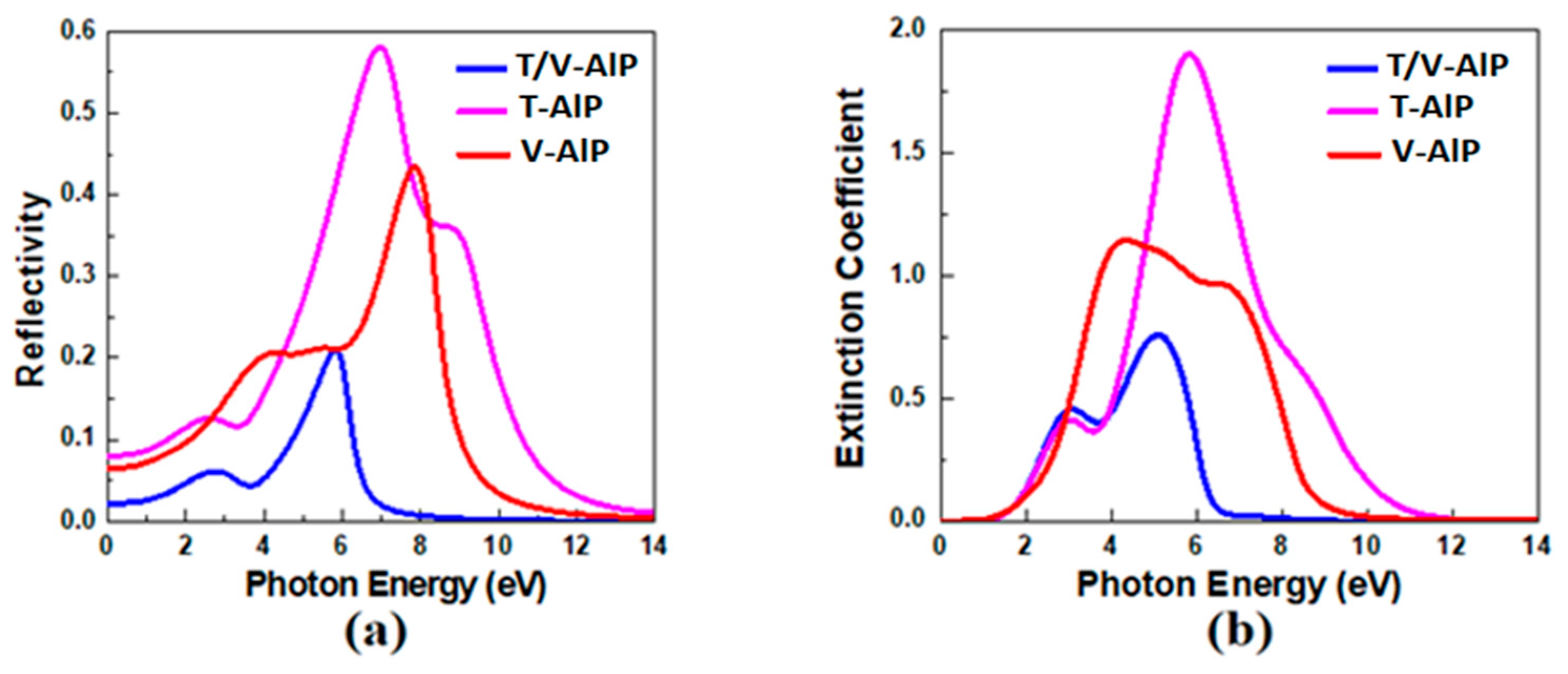
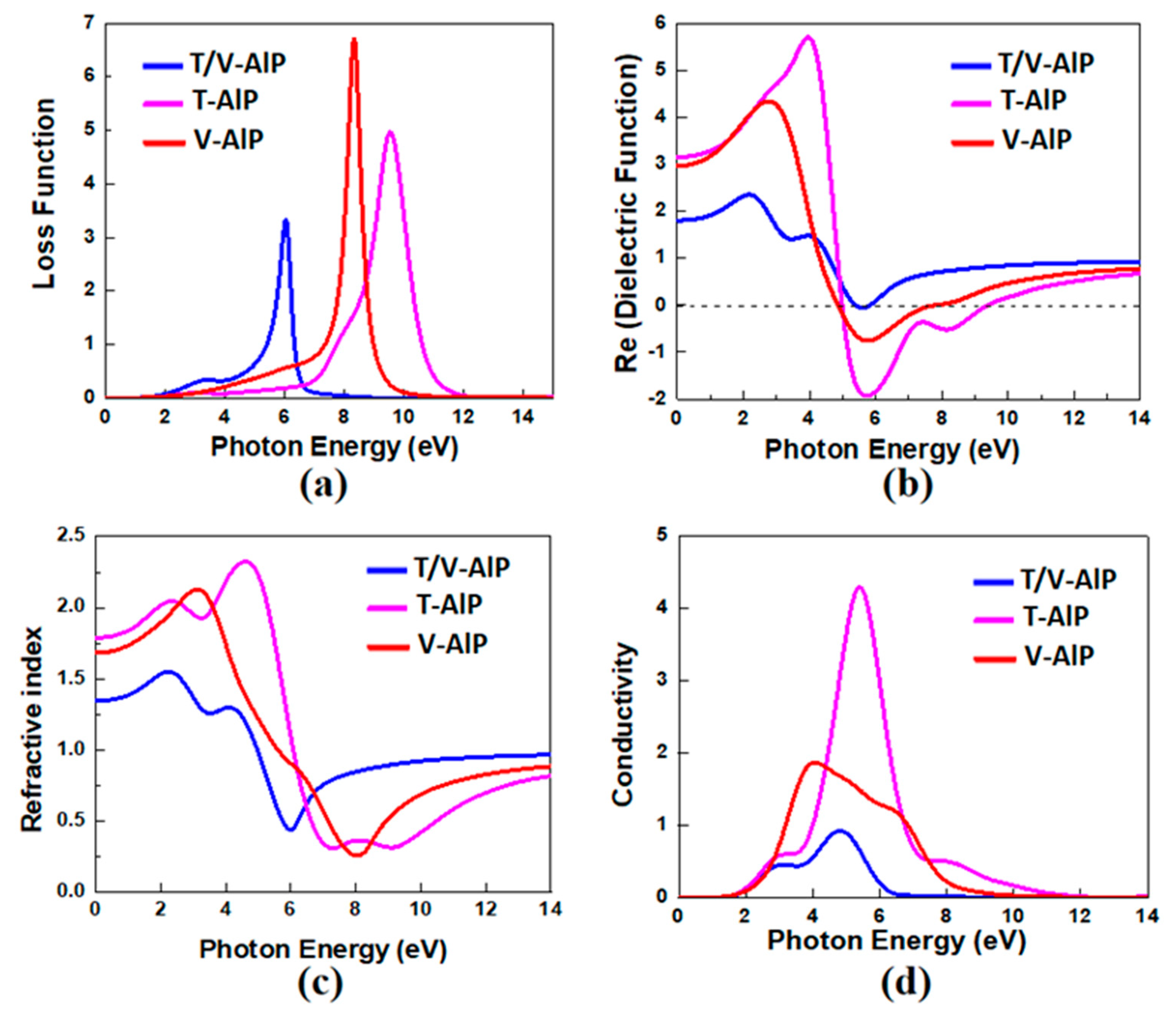
3.3. Optical Properties

The optical properties can be described by the dielectric function as ε ( ω ) = ε 1 ( ω ) + i ε 2 ( ω ) . The imaginary part of the dielectric function ε 2 ( ω ) is an important factor of 2D material, which contains much information about the energy band structure, and various optical spectra can be calculated from it. We plotted the dielectric functions and absorption coefficients, the reflectivity and the extinction coefficient of the three types of AlP bilayers in Figure 9. It can be seen in Figure 9a that the imaginary part of the dielectric function of AlP bilayers exhibits different peaks; the corresponding photon energies are 2.93 eV, 4.70 eV for the T/V-AlP bilayer, 4.74, 7.56 for the T-AlP bilayer and 3.98 eV for the V-AlP bilayer, respectively. It is clear that the peak of the T/V-AlP bilayer is much higher than the others. Compared with the V-AlP and T-AlP bilayers, the first dielectric peak of T/V-AlP shows a slight shift (red shift), which corresponds to the narrow band gap in Figure 3. It was found that ε 2 ( ω ) has two obvious peaks except for the V-AlP bilayer. The dielectric peak of V-AlP first rises significantly, arriving at its top value at an energy of 3.98 eV, and in the following it falls obviously. The absorption spectra of different AlP bilayers are shown in Figure 9b. The V-AlP bilayer exhibits the highest absorption spectrum peak among the three types of AlP bilayers. It can be seen in Figure 9b that the absorption function of AlP bilayers exhibits different peaks; the corresponding photon energies are 5.23 eV for the T/V-AlP bilayer, 5.43 eV, 8.00 eV for the T-AlP bilayer and 5.51 eV for V-AlP bilayer, respectively. These absorption peaks with the energies of 5.23 eV and 8.00 eV lie in the ultraviolet (UV) range (10–400 nm), indicating these AlP bilayers have potential applications in the UV and far-UV light detector fields.
It can be seen in Figure 10a that the reflectivity of the AlP bilayers exhibits different peaks; the corresponding photon energies are 3.4 eV and 6.0 eV for the T/V-AlP bilayer, 9.5 eV for the T-AlP bilayer and 8.3 eV for the V-AlP bilayer, respectively. From Figure 10b, it is found that the extinction coefficient of AlP bilayers exhibits five different peaks; the corresponding photon energies are 3.1 eV and 5.1 eV for the T/V-AlP bilayer, 3.0 eV and 5.8 eV for the T-AlP bilayer and 4.3 eV for the V-AlP bilayer, respectively.
The remaining optical spectra of the AlP bilayers, such as loss function, refractive index and conductivity, are shown in Figure 11. They are also important factors in evaluating the AlP bilayers and their optical applications. From Figure 11a, it is found that the energy loss peaks’ energy positions are in agreement with those of the reflectivity spectrum tail edge. It is found that the energy loss of the AlP bilayers exhibits four different peaks; the corresponding photon energies are 3.4 eV and 6.0 eV for the T/V-AlP bilayer, 9.5 eV for the T-AlP bilayer and 8.3 eV for the V-AlP bilayer, respectively. The loss function spectrum peaks and reflectivity spectrum peaks of these AlP bilayers all emerge at the energy position of 6.0 eV, 9.5 eV and 8.3 eV. In Figure 11b, it can be seen that the real part of the dielectric function in the T-AlP bilayer is negative in the range from 5.0 eV to 9.4 eV. Additionally, that of the V-AlP bilayer is negative in the range of 4.7–7.7 eV. Figure 11b also shows the real dielectric spectrums of the T/V-AlP bilayer, and it can be found that the transition between the dielectric property and the metallic property will happen when the photon energy changes at approximately 4.0 eV and 10.0 eV.
The refractive index and conductivity spectra of AlP bilayers are plotted in Figure 11c,d. As shown in Figure 11c, the real refractive index of AlP bilayers are 1.34, 1.79 and 1.68 for the T/V-AlP, T-AlP and V-AlP bilayers, respectively. It can be seen from Figure 10b and Figure 11d that the curves of the conductivity spectra of AlP bilayers have similar shapes to their extinction coefficient spectra, and their peaks also have the same energy positions.

4. Conclusions

In summary, we have systematically studied the electronic band structure and optical properties of the three types of AlP bilayers. The high stabilities of the three types of AlP bilayers are proved by considering their binding energy. Interestingly, the T-AlP and V-AlP bilayers both possess direct band gaps, which are useful in nanoelectronic devices. These band gaps exhibit remarkably diverse behavior induced by changes to the biaxial strain applied. Under biaxial strain, the electronic band structures and band gaps of AlP bilayers can be tuned in different ranges. In particular, the indirect energy band gap of the T/V-AlP bilayer is tuned into a direct band gap by applying biaxial compressive strain. The tunable range of the direct band gap of the T-AlP bilayer is from 1.06 eV to 1.55 eV, that of the T/V-AlP bilayer is from 0 eV to 1.16 eV, and that of the V-AlP bilayer is from 0 eV to 1.9 eV. The AlP bilayers show novel optical properties, especially strong light absorption in the UV range of the sunlight spectrum. Therefore, these 2D AlP bilayers have potential applications in nanoelectronic fields. These results provide important reference and information for the design of new nanoelectric devices based on AlP materials.

Supplementary Materials

The following supporting information can be downloaded at: https://www.mdpi.com/article/10.3390/cryst13040597/s1, Table S1: Mulliken layout analysis of T-AlP, V-AlP and T/V-AlP bilayers; Figure S1: The electron density difference maps of (a) T-AlP, (b) V-AlP and (c) T/V-AlP bilayers. The top view and front view are both displayed for each AlP bilayer.

Author Contributions

Conceptualization, C.M. and Y.H.; methodology, H.N.; validation, L.Q.; formal analysis, H.N.; investigation, C.M. and Y.H.; resources, L.Q. and Y.H.; data curation, H.H.; writing—original draft preparation, C.M. and Y.H.; writing—review and editing, Y.H. and H.N.; visualization, H.N. and H.H.; supervision, Y.H.; project administration, C.M.; funding acquisition, Y.H. and L.Q. All authors have read and agreed to the published version of the manuscript.

Funding

This research was funded by the Research Foundation of Educational Commission of Hubei Province, grant number B2020153, the Scientific Research Project and Innovation Team of Hubei University of Science and Technology, grant number HKCXTD-001, the Research Project of Hubei Key Laboratory of Radiation Chemistry and Functional Materials and Hubei University of Science and Technology, grant number 2021ZX02, 2020-21X26 and 2020-22GP01, the National Undergraduate Innovation and Entrepreneurship Plan Training Program, grant number 202210927002, the Key Incubation Projects for Innovation and Entrepreneurship at Hubei University of Science and Technology, grant number 2022-026 and the Program for Science and Technology Innovation Team in Colleges of Hubei Province, grant number T2021012.

Data Availability Statement

The data presented in this study are available upon request.

Conflicts of Interest

The authors declare no conflict of interest.

References

  1. Novoselov, K.S.; Geim, A.K.; Morozov, S.V.; Jiang, D.; Zhang, Y.; Dubonos, S.V.; Grigorieva, I.V.; Firsov, A.A. Electric field effect inatomically thin carbon films. Science 2004, 306, 666–669. [Google Scholar] [CrossRef] [Green Version]
  2. Huang, Y.; Zhu, C.; Zhang, S.; Hu, X.; Zhang, K.; Zhou, W.; Guo, S.; Xu, F.; Zeng, H. Ultrathin Bismuth Nanosheets for Stable Na-Ion Batteries: Clarification of Structure and Phase Transition by in Situ Observation. Nano Lett. 2019, 19, 1118–1123. [Google Scholar] [CrossRef] [PubMed]
  3. Ashton, M.; Mathew, K.; Hennig, R.G.; Sinnott, S.B. Predicted Surface Composition and Thermodynamic Stability of MXenes in Solution. J. Phys. Chem. C 2016, 120, 3550–3556. [Google Scholar] [CrossRef]
  4. Ashton, M.; Paul, J.; Sinnott, S.B.; Hennig, R.G. Topology-Scaling Identification of Layered Solids and Stable Exfoliated 2D Materials. Phys. Rev. Lett. 2017, 118, 10610. [Google Scholar] [CrossRef] [PubMed] [Green Version]
  5. Geim, A.K. Graphene: Status and Prospects. Science 2009, 324, 1530–1534. [Google Scholar] [CrossRef] [Green Version]
  6. Zhang, Y.; Dong, N.; Tao, H.; Yan, C.; Huang, J.; Liu, T.; Robertson, A.W.; Texter, J.; Wang, J.; Sun, Z.Y. Exfoliation of stable 2D black phosphorus for device fabrication. Chem. Mater. 2017, 29, 6445–6456. [Google Scholar] [CrossRef]
  7. Zhang, S.; Guo, S.; Ma, Y.; Chen, Z.; Wang, Y.; Gao, H.; Herrero, J.G.; Ares, P.; Zamora, F.; Zhou, Z.; et al. Recent progress in 2D group-VA semiconductors: From theory to experiment. Chem. Soc. Rev. 2018, 47, 982–1021. [Google Scholar] [CrossRef] [Green Version]
  8. Niu, T.; Zhou, W.; Zhou, D.; Hu, X.; Zhang, S.; Zhang, K.; Zhou, M.; Fuchs, H.; Zeng, H. Modulating Epitaxial Atomic Structure of Antimonene through Interface Design. Adv. Mater. 2019, 31, 1902606. [Google Scholar] [CrossRef]
  9. Zhang, Y.; Liu, W.; Niu, H. Half-metallic ferromagnetism in Cr-doped AlP—Density functional calculations. Solid State Commun. 2008, 145, 590–593. [Google Scholar] [CrossRef]
  10. Zhang, Y. Possible room temperature ferromagnetism in Ca-doped AlP: First-principles study. J. Magn. Magn. Mater. 2013, 342, 35–37. [Google Scholar] [CrossRef]
  11. Liang, P.; Liu, Y.; Hu, X.; Wang, L.; Dong, Q.; Jing, X. The half metallic property and electronic structure of the Ti doped AlP systems investigated by first principle. J. Magn. Magn. Mater. 2014, 355, 295–299. [Google Scholar] [CrossRef]
  12. Yan, Z.; Wu, H.; Zheng, R. Ferromagnetism in alkali-metal-doped AlP: An ab initio study. Comput. Mater. Sci. 2015, 99, 16–20. [Google Scholar] [CrossRef]
  13. Boutaleb, M.; Doumi, B.; Tadjer, A.; Sayede, A. Half-metallic ferromagnetic properties of Cr- and V-doped AlP semiconductors. J. Magn. Magn. Mater. 2016, 397, 132–138. [Google Scholar] [CrossRef]
  14. Wang, S.; Fan, X.; An, Y. Room-temperature ferromagnetism in alkaline-earth-metal doped AlP: First-principle calculations. Comput. Mater. Sci. 2018, 142, 338–345. [Google Scholar] [CrossRef]
  15. Chen, Y.; Xing, Y.; Jiang, A.; Zhou, C.; Lu, S. Enhanced optical absorption in visible range in Mn doped AlP: A density functional theory study. J. Magn. Magn. Mater. 2018, 457, 13–16. [Google Scholar] [CrossRef]
  16. Sun, J. Stability and Electronic Structures of Single-Walled Alp Nanotubes by First Principle Study. Procedia Eng. 2011, 15, 5062–5066. [Google Scholar]
  17. Tong, C.; Zhang, H.; Zhang, Y.; Liu, H.; Liu, L. New manifold two-dimensional single-layer structures of zinc-blende compounds. J. Mater. Chem. A 2014, 2, 17971–17978. [Google Scholar] [CrossRef]
  18. Liu, C.; Teng, Z.; Ye, X.; Yan, X. Two-dimensional tetragonal AlP monolayer: Strain-tunable direct–indirect band-gap and semiconductor–metal transitions. J. Mater. Chem. C 2017, 5, 5999–6004. [Google Scholar] [CrossRef]
  19. Yang, X.; Mao, C.; Hu, Y.; Cao, H.; Zhang, Y.; Zhao, D.; Chen, Z.; Xie, M. Two-dimensional aluminum phosphide semiconductor with tunable direct band gap for nanoelectricapplications. RSC Adv. 2020, 10, 25170–25176. [Google Scholar] [CrossRef]
  20. Vanderbilt, D. Soft self-consistent pseudopotentials in a generalized eigenvalue formalism. Phys. Rev. B 1990, 41, 7892–7895. [Google Scholar] [CrossRef]
  21. Perdew, J.P.; Zunger, A. Self-interaction correction to density-functional approximations for many-electron systems. Phys. Rev. B 1981, 23, 5048–5079. [Google Scholar] [CrossRef] [Green Version]
  22. Perdew, J.P.; Burke, K.; Ernzerhof, M. Generalized gradient approximation made simple. Phys. Rev. Lett. 1996, 77, 3865–3868. [Google Scholar] [CrossRef] [PubMed] [Green Version]
  23. Heyd, J.; Scuseria, G.E.; Ernzerhof, M. Hybrid functionals based on a screened Coulomb potential. J. Chem. Phys. 2003, 118, 207–8215. [Google Scholar] [CrossRef] [Green Version]
  24. Monkhorst, H.J.; Pack, J.D. Special points for Brillouin-zone integration. Phys. Rev. B 1976, 13, 5188–5192. [Google Scholar] [CrossRef]
  25. Tkatchenko, A.; Scheffler, M. Accurate molecular van der Waals interactions from ground-state electron density and free-atom reference data. Phys. Rev. Lett. 2009, 102, 073005. [Google Scholar] [CrossRef] [Green Version]
  26. Mao, Y.; Xu, C.; Yuan, J.; Zhao, H. Effect of stacking order and in-plane strain on the electronic properties of bilayer GeSe. Phys. Chem. Chem. Phys. 2018, 20, 6929–6935. [Google Scholar] [CrossRef]
  27. Zhang, K.; Feng, S.; Wang, J.; Azcatl, A.; Lu, N.; Addou, R.; Wang, N.; Zhou, C.; Lerach, J.; Bojan, V. Correction to manganese doping of monolayer MoS2: The substrate is critical. Nano Lett. 2016, 16, 2125. [Google Scholar] [CrossRef]
  28. Qu, H.; Zhou, W.; Guo, S.; Li, Z.; Wang, Y.; Zhang, S. Ballistic Quantum Transport of Sub-10 nm 2D Sb2Te2Se Transistors. Adv. Bioelectron. Mater. 2019, 5, 1900813. [Google Scholar] [CrossRef]
  29. Zhang, S.; Hu, Y.; Hu, Z.; Cai, B.; Zeng, H. Hydrogenated arsenenes as planar magnet and Dirac material. Appl. Phys. Lett. 2015, 107, 022102. [Google Scholar] [CrossRef]
  30. Choi, S.M.; Jhi, S.H.; Son, Y.W. Effects of strain on electronic properties of graphene. Phys. Rev. B 2010, 81, 081407. [Google Scholar] [CrossRef] [Green Version]
Figure 1. The geometry structures of (a) T-AlP; (b) V-AlP and (c) T/V-AlP bilayers. The two symbols a and b are lattice parameters. The symbols λ and Δ represent vertical distances between the inner- and outer-layer atoms respectively.
Crystals 13 00597 g001
Figure 2. The total energy of the three systems versus the interlayer distance. (a) The case for T/V-AlP bilayers; (b) the case for T-AlPand V-AlP bilayers.
Crystals 13 00597 g002
Figure 3. Energy band structures of T-AlP, V-AlP and T/V-AlP bilayers. In (a,b), the vertical arrows represent the direct band gaps of T-AlP and V-AlP materials, and the diagonal arrow in (c) represents indirect band gap of the T/V-AlP heterojunction. The horizontal dotted line represents Femi level and the light green areas denote the bandgap.
Crystals 13 00597 g003
Figure 4. The PDOS of (a) T-AlP, (b) V-AlP and (c) T/V-AlP bilayers. The vertical dotted line represents Femi level.
Crystals 13 00597 g004
Figure 5. The band gaps of the T-AlP, V-AlP and T/V-AlP bilayers versus biaxial strain. The vertical dotted line corresponds to the unstressed condition. The biaxial strain step is 2% in our work.
Crystals 13 00597 g005
Figure 6. Changes in the electronic band structure for the T-AlP bilayer influenced by external strain of (af) ε = −12%, −8%, −4%, 4%, 8%, and 12%. Here and in the following, the vertical arrow represents the direct band gap, and the diagonal arrow represents the indirect band gap. The horizontal dotted line represents Femi level.
Crystals 13 00597 g006
Figure 7. Band structure change for the V-AlP bilayer induced by external biaxial strain. Five cases, including figures (ae), show the direct band gaps (vertical arrows), while (f) shows an indirect band gap (diagonal arrow).
Crystals 13 00597 g007
Figure 8. Band structure change and the band edge shift under biaxial strain for the T/V-AlP bilayer based on HSE functional. In the case of compression, figures (ac) show direct band gaps (vertical arrows), while in the case of tension, figures (df) show indirect band gaps (diagonal arrows).
Crystals 13 00597 g008
Figure 9. (a) The imaginary dielectric function; (b) the absorption spectra of the AlP bilayers. Curves of different colors represent the optical spectra of the different types of AlP bilayer materials.
Crystals 13 00597 g009
Figure 10. (a) The reflectivity and (b) the extinction coefficient of the three types of AlP bilayers.
Crystals 13 00597 g010
Figure 11. (a) The loss function; (b) the real part of dielectric function; (c) the refractive index and (d) the conductivity of the three types of AlP bilayers.
Crystals 13 00597 g011
Table 1. The parameters of the 2D AlP crystals: lattice parameter (a and b), average bond lengths (l), cohesive energy (Ecoh) and band gap (Eg). The unit of energy is electron volts (eV), and that of length is angstroms (Å). Thickness Δ (Å) is defined by the vertical distance and it is shown in Figure 1. The distance λ (Å) between the upper layer and the lower layer is defined by the vertical distance between the lower- and upper-layer atoms in these 2D material models, as is also shown in Figure 1.
Model a , b (Å) l Δ λ E c o h E g
V-AlP monolayer a  = 3.81, b  = 5.682.322.2---−5.122.62
T-AlP monolayer a  = b  = 3.912.432.9---−5.350.97
V-AlP bilayer a  = 3.81, b  = 5.682.346.21.6−5.001.86
T-AlP bilayer a  = b  = 3.892.278.83.6−4.851.29
T/V-AlP bilayer a  = 3.85, b  = 28.42.378.63.4−4.940.86
Disclaimer/Publisher’s Note: The statements, opinions and data contained in all publications are solely those of the individual author(s) and contributor(s) and not of MDPI and/or the editor(s). MDPI and/or the editor(s) disclaim responsibility for any injury to people or property resulting from any ideas, methods, instructions or products referred to in the content.

