
Ab-Initio Calculation of the Electrical Conductivity, Optical Absorption, and Reflectivity of the 2D Materials SnC and NbC

Abstract
:1. Introduction
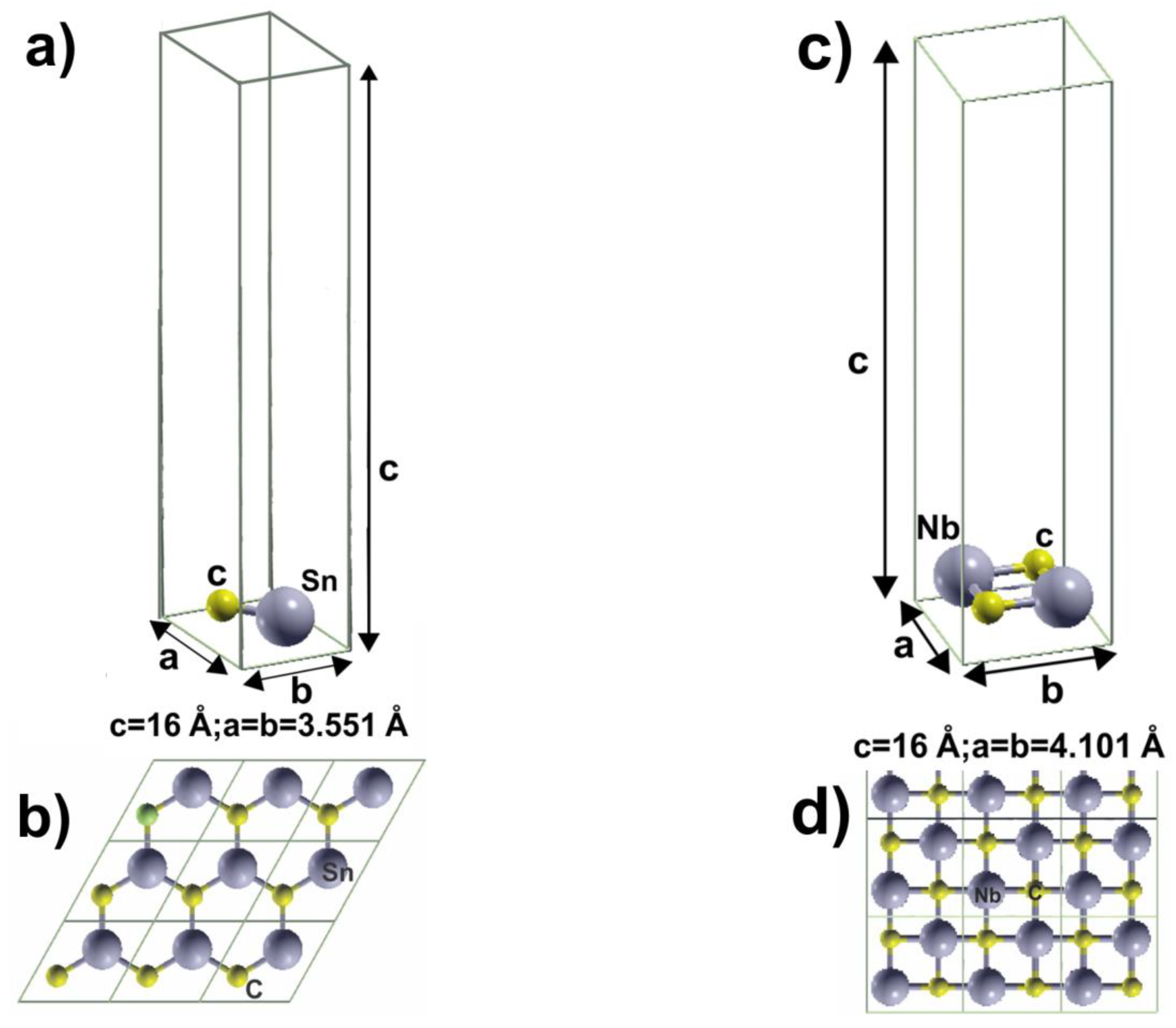
2. Materials and Methods
3. Results
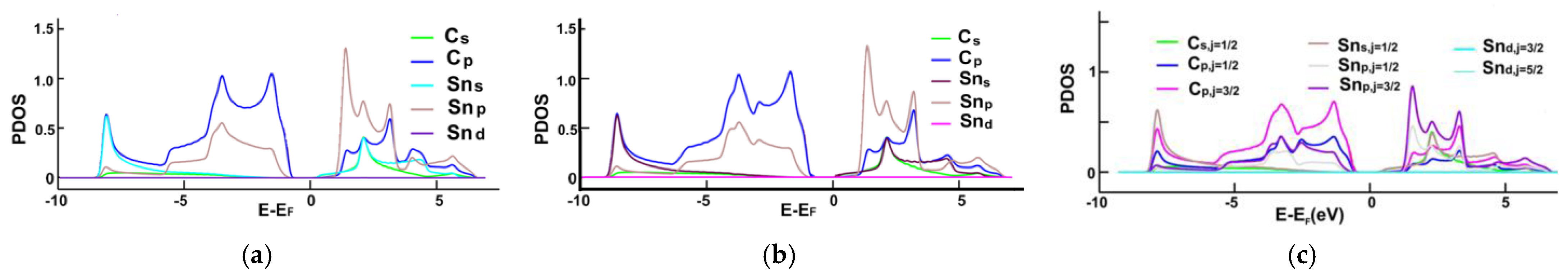
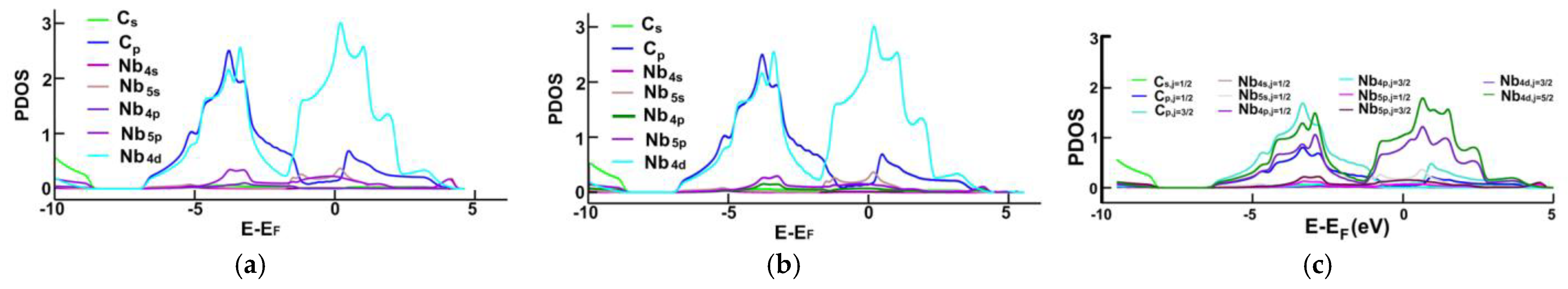
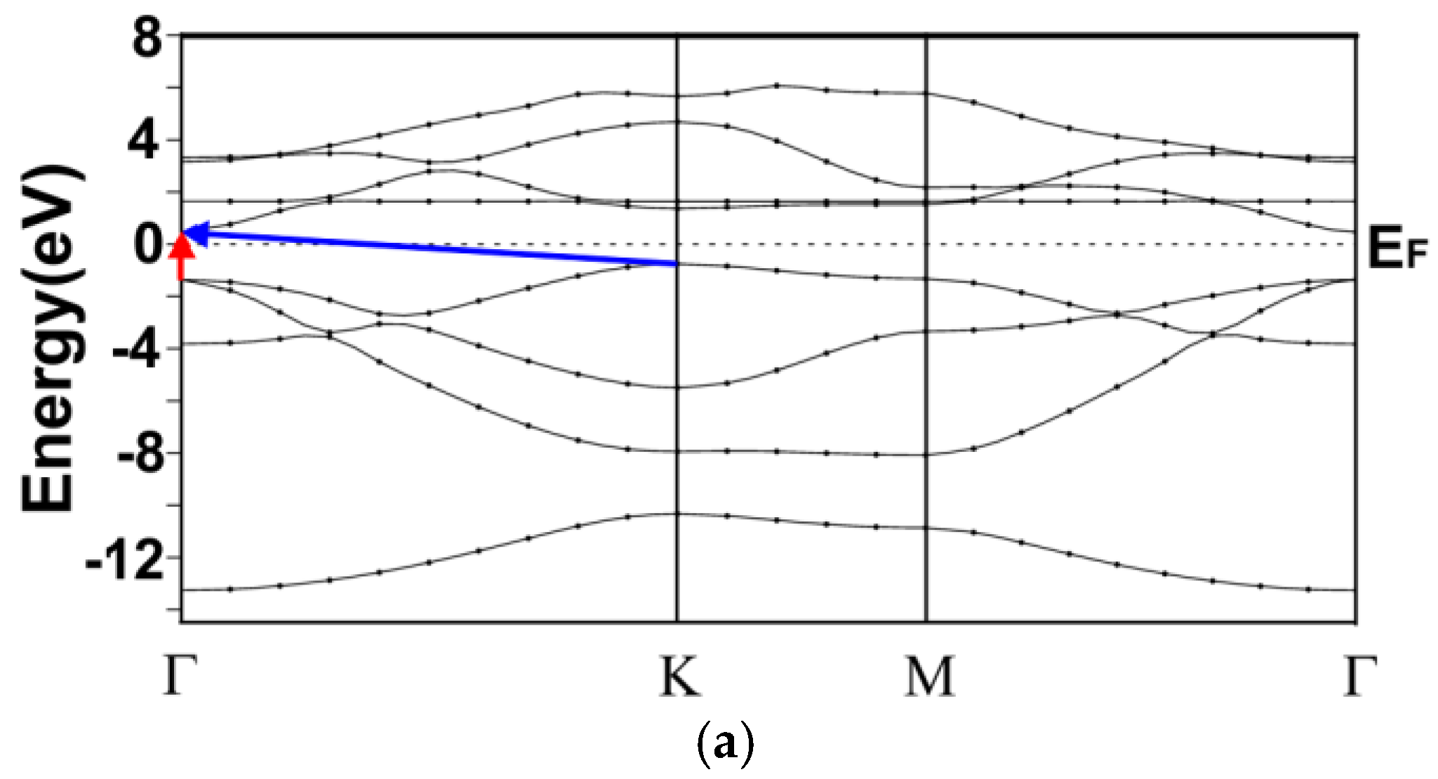
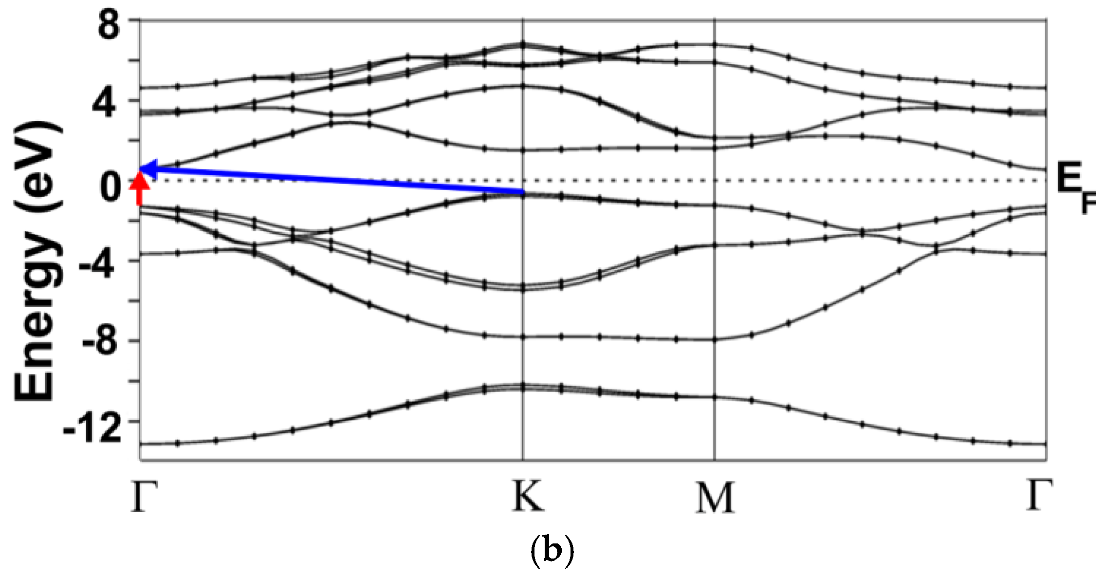
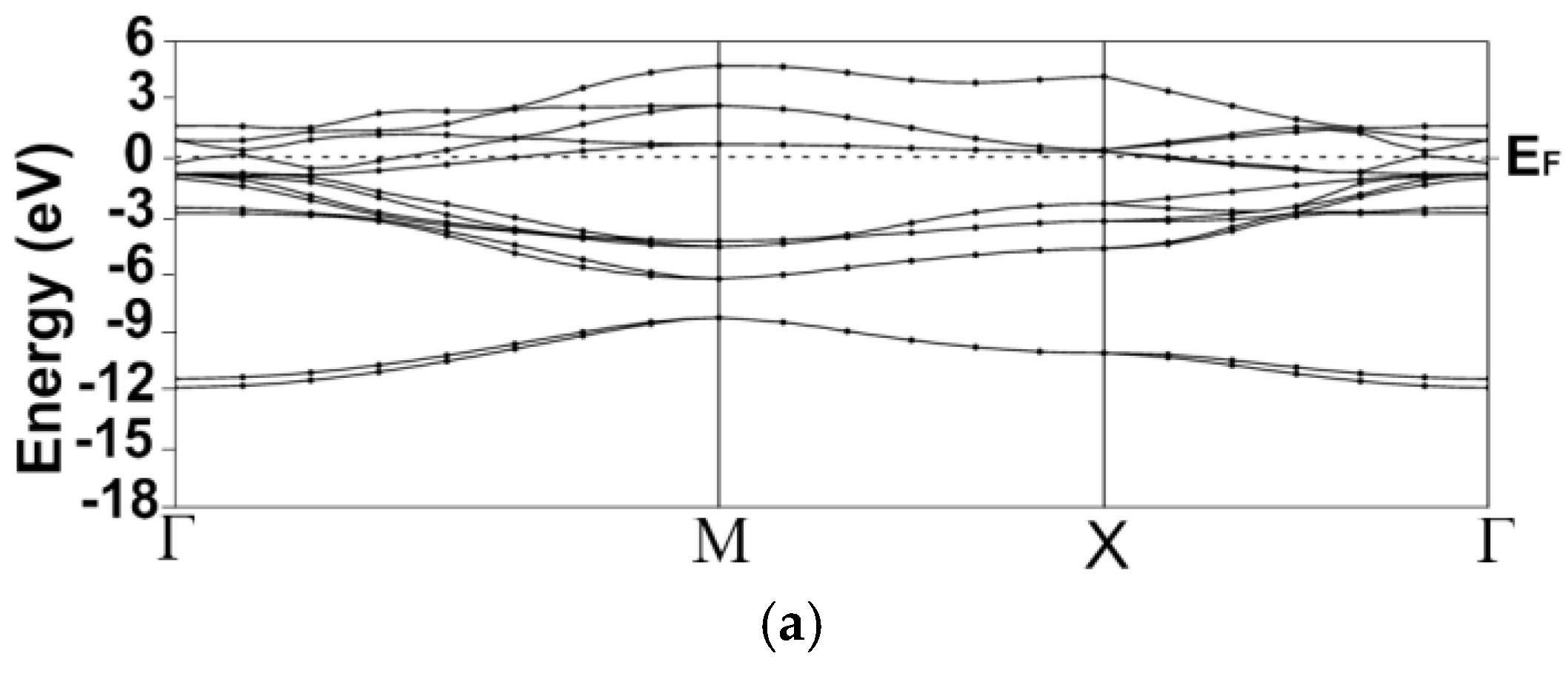
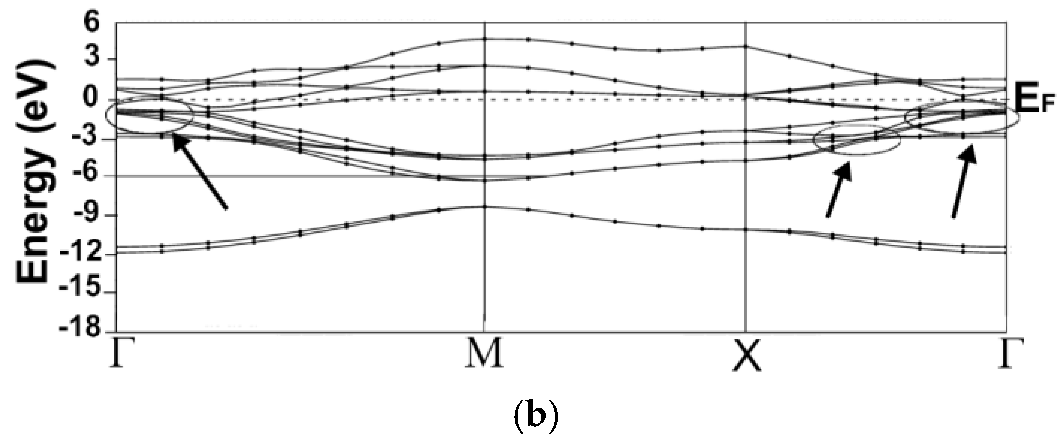
3.1. Energy Band Structures and Electrical Conductivities
3.2. Optical Properties
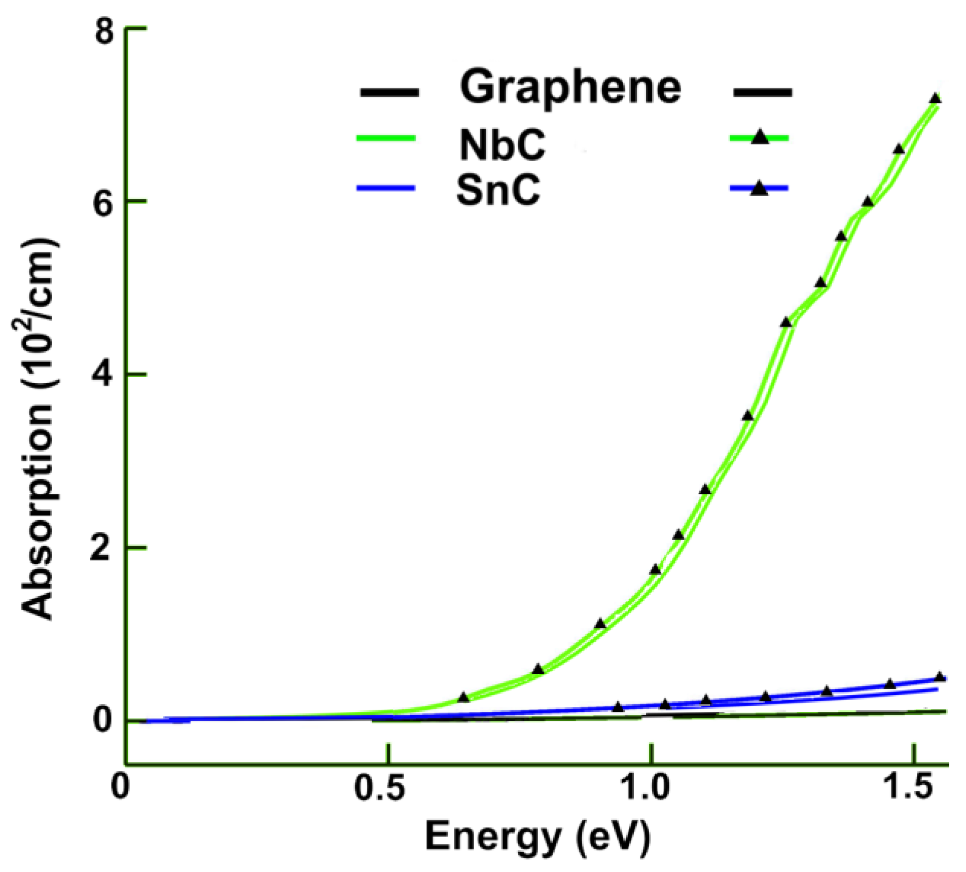
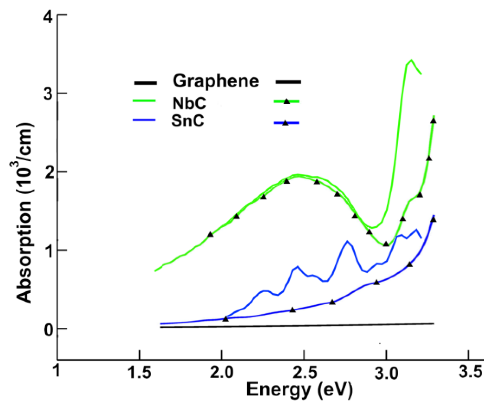
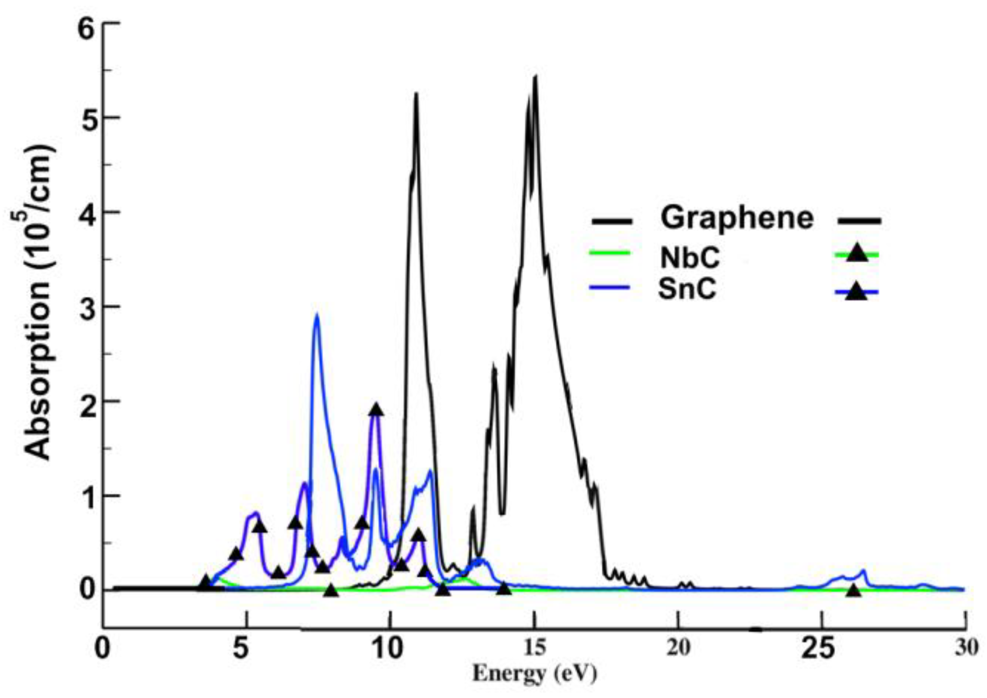
3.2.1. Absorption
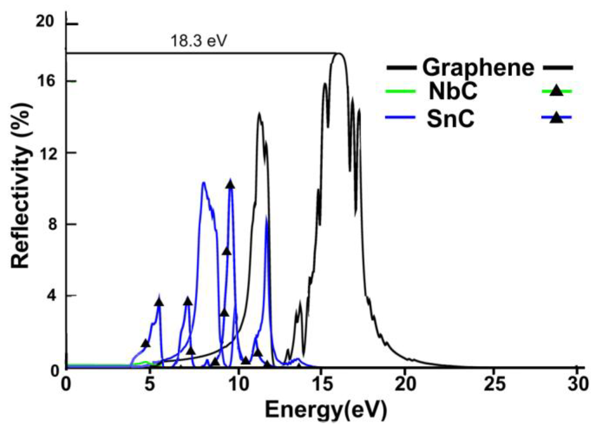
3.2.2. Reflectivity
4. Discussion
Author Contributions
Funding
Data Availability Statement
Acknowledgments
Conflicts of Interest
References
- Williams, W.S. The thermal conductivity of metallic ceramics. JOM 1998, 50, 62–66. [Google Scholar] [CrossRef]
- Zhang, B.; Huang, Y.; Bao, W.; Wang, B.; Meng, Q.; Fan, L.; Zhang, Q. Two-dimensional stable transition metal carbides (MnC and NbC) with prediction and novel functionalizations. Phys. Chem. Chem. Phys. 2018, 20, 25437–25445. [Google Scholar] [CrossRef] [PubMed]
- Cuppari, M.G.D.V.; Santos, S.F. Physical Properties of the NbC Carbide. Metals 2016, 6, 250. [Google Scholar] [CrossRef]
- Benzair, A.; Bouhafs, B.; Khelifa, B.; Mathieu, H.; Aourag, H. The ground state and the bonding properties of the hypothetical cubic zinc-blende-like GeC and SnC Compounds. Phys. Let. A 2001, 282, 299–308. [Google Scholar] [CrossRef]
- Khenata, R.; Baltache, H.; Sahnoun, M.; Driz, M.; Rérat, M.B.; Abbar, B. Full potential linearized augmented plane wave calculations of structural and electronic properties of GeC, SnC and GeSn. Phys. B 2003, 336, 321–328. [Google Scholar] [CrossRef]
- Hoat, D.M.; Naseri, M.; Ponce-Péreze, R.; Hieu, N.N.; Rivas-Silva, J.F.; Vu, T.V.; Tong, H.D.; Cocoletzi, G.H. Structural and electronic properties of chemically functionalized SnC monolayer: A first principles study. Mater. Res. Express 2020, 7, 015013. [Google Scholar] [CrossRef]
- Rehman, J.; Fan, X.; Zheng, W.T. 2D SnC sheet with a small strain is a promising Li host material for Li-ion batteries. Mater. Today Commun. 2021, 26, 101768. [Google Scholar] [CrossRef]
- Butt, M.K.; Zeeshan, H.M.; Dinh, V.A.; Zhao, Y.; Wang, S.; Jin, K. Monolayer SnC as anode material for Na ion batteries. Comput. Mater. Sci. 2021, 197, 110617. [Google Scholar] [CrossRef]
- Giannozi, P.; Baroni, S.; Bonini, N.; Calandra, M.; Car, R.; Cavazzoni, C.; Ceresoli, D.; Chiarotti, G.L.; Cococcioni, M.; Dabo, I.; et al. QUANTUM ESPRESSO: A Modular and Open-Source Software Project for Quantum Simulations of Materials. J. Phys. Condens. Matter 2009, 21, 395502. [Google Scholar] [CrossRef] [PubMed]
- Troullier, N.; Martins, J.L. Efficient Pseudopotentials for Plane-Wave Calculations. Phys. Rev. B 1991, 43, 1993–2006. [Google Scholar] [CrossRef] [PubMed]
- Perdew, J.P.; Burke, K.; Ernzerhof, M. Generalized Gradient Approximation Made Simple. Phys. Rev. Lett. 1996, 77, 3865–3868. [Google Scholar] [CrossRef] [PubMed]
- Monkhorst, H.J.; Pack, J.D. Special Points for Brillouin-Zone Integrations. Phys. Rev. B 1976, 13, 5188–5192. [Google Scholar] [CrossRef]
- Lide, D.R. CRC Handbook of Chemistry and Physics: A Ready-Reference Book of Chemical and Physical Data, 81st ed.; CRC Press: Boca Raton, FL, USA, 2000; pp. 2000–2001. ISBN 978-0-8493-0481-1. [Google Scholar]
- Kumar, S.; Maurya, T.K.; Auluck, S. Electronic and optical properties of ordered BexZn 1-xSe alloys by the FPLAPW method. J. Phys. Condens. Matter 2008, 20, 075205. [Google Scholar] [CrossRef]
- Kittel, C. Introduction to Solid State Physics, 3rd ed.; John Wiley: New York, NY, USA, 1966; p. 648. [Google Scholar]
- Salas, O.; Garcés, E.; Magana, L.F. The Interaction of the 2D MoP2 and NbP2 Surfaces with Carbon Dioxide and Carbon Monoxide and Changes in their Optical Properties. Crystals 2022, 12, 45. [Google Scholar] [CrossRef]
- Mostofi, A.A.; Yates, J.R.; Pizzi, G.; Lee, Y.S.; Souza, I.; Vanderbilt, D.; Marzari, N. A tool for obtaining maximally- localized Wannier functions. Comput. Phys. Commun. 2014, 185, 2309. [Google Scholar] [CrossRef]
- Pizzi, G.; Volja, D.; Kozinsky, B.; Fornari, M.; Marzari, N. Boltzwann: A code for the evaluation of thermoelectric and electronic transport properties with a maximally localized Wannier functions basis. Comput. Phys. Commun. 2014, 185, 422–429. [Google Scholar] [CrossRef]
- Islam, M.R.; Wang, Z.; Qu, S.; Liu, K.; Wang, Z. The impact of spin-orbit coupling and the strain effect on monolayer tin carbide. J. Comput. Electron. 2021, 20, 151. [Google Scholar] [CrossRef]


Disclaimer/Publisher’s Note: The statements, opinions and data contained in all publications are solely those of the individual author(s) and contributor(s) and not of MDPI and/or the editor(s). MDPI and/or the editor(s) disclaim responsibility for any injury to people or property resulting from any ideas, methods, instructions or products referred to in the content. |
© 2023 by the authors. Licensee MDPI, Basel, Switzerland. This article is an open access article distributed under the terms and conditions of the Creative Commons Attribution (CC BY) license (https://creativecommons.org/licenses/by/4.0/).
Share and Cite
Delgado, N.; Salas, O.; Garcés, E.; Magaña, L.F. Ab-Initio Calculation of the Electrical Conductivity, Optical Absorption, and Reflectivity of the 2D Materials SnC and NbC. Crystals 2023, 13, 682. https://doi.org/10.3390/cryst13040682
Delgado N, Salas O, Garcés E, Magaña LF. Ab-Initio Calculation of the Electrical Conductivity, Optical Absorption, and Reflectivity of the 2D Materials SnC and NbC. Crystals. 2023; 13(4):682. https://doi.org/10.3390/cryst13040682
Chicago/Turabian StyleDelgado, Nadxiieli, Osiris Salas, Erick Garcés, and Luis Fernando Magaña. 2023. "Ab-Initio Calculation of the Electrical Conductivity, Optical Absorption, and Reflectivity of the 2D Materials SnC and NbC" Crystals 13, no. 4: 682. https://doi.org/10.3390/cryst13040682