
Epitaxial Integration of Dirac Semimetals with Si(001)

National Renewable Energy Laboratory, Golden, CO 80401, USA
*
Author to whom correspondence should be addressed.
Crystals 2023, 13(4), 578; https://doi.org/10.3390/cryst13040578
Submission received: 16 February 2023
/
Revised: 11 March 2023
/
Accepted: 21 March 2023
/
Published: 28 March 2023
(This article belongs to the Special Issue Epitaxial Growth of Semiconductor Materials and Devices)
Abstract
:Topological semimetals contain novel combinations of properties that make them useful in a variety of applications, including optoelectronics, spintronics and low energy computing, and catalysis. Although they have been grown with high quality as bulk single crystals, incorporation with semiconductor substrates will ultimately be required to maximize their technological reach. Here, epitaxial growth of the Dirac semimetal CdAs on Si(001) is demonstrated through two routes. First, CdAs(112) epilayers are grown on Si(001) via an intermediate CdTe(111) buffer layer. Second, CdAs(112) is grown directly on Si(001). This work sets the foundation for integration of novel semimetal materials with existing CMOS technology.
1. Introduction
Topological semimetals offer a unique combination of properties relevant for a wide variety of applications. Dirac semimetals, which contain pairs of degenerate, linear band crossings, present high electron mobilities [1], broadband light absorption [2], fast carrier dynamics, and low thermal conductivities [3]. Weyl semimetals, in which the pairs of nodes are non-degenerate and of opposite chirality, share many of these same properties, along with added sensitivity to light polarization [4] and the potential to exhibit large spin Hall angles [5]. Such properties are advantageous for photodetectors [6,7], optical switches [8], spin-orbit torque devices [5], thermoelectrics [9,10,11], and catalysts [12]. Additionally, the surface and bulk electronic states have topological protection arising from the symmetry of the crystal, resulting in increased robustness from a variety of defects and scattering mechanisms [4]. Many of these materials were initially synthesized as bulk crystals, allowing for the study of their basic properties. Advances in thin film synthesis and integration with semiconductor device structures are now required to access and utilize their unique properties in devices.
Thin film synthesis of the Dirac semimetal CdAs by molecular beam epitaxy (MBE) has yielded the highest mobility thin film semimetals to date. CdAs has a tetragonal crystal structure (a = b = 1.26 nm and c = 2.54 nm) [13,14], making it amenable to epitaxy on zinc blende and diamond lattices. Although bulk single crystals have the highest reported mobilities [1], much progress has been on tailoring growth approaches on conventional substrates to minimize extended defects, while also achieving lower carrier concentrations. The atomic arrangement of its lowest energy (112) surface is similar to that of (111) zinc blende surfaces, and high quality growth was first achieved on GaAs(111) substrates [15]. Since then, epitaxy has also been carried out on GaSb(001) [16] and commercially relevant GaAs(001) [7,17] substrates, presenting clear pathways to designing and fabricating integrated device structures. Combined with II-Te or III-Sb buffer layers, all have templated the growth of CdAs with room temperature mobilities of 10,000–20,000 cm. A key enabling feature has been the use of lattice-matched buffer layers to reduce relaxation-induced defect formation. The next frontier in harnessing the properties of topological semimetals is to grow them on Si(001) substrates.
Integration of topological semimetals with Si offers two distinct possibilities, among others. First, it could enable the incorporation of optoelectronic functionality into Si-based devices. Significant effort has been made recently to incorporate III–V compounds with Si. However, the low defect tolerance of III–V devices require growth strategies to minimize defect formation, such as using anti-phase domain free GaP [18], or quantum dot structures, such as InAs on GaAs, that can withstand high defect densities better than typical quantum wells due to the dots’ ability to emit independently of each other [19]. Expanding the selection of materials that offer greater defect tolerance and additional functionality will help to advance optoelectronic device technologies, including photodetectors. The reduced dependence of electron mobility on dislocation density in CdAs [20] and demonstration of photodetectors [7] despite greater than 10 cm dislocation densities indicate that topological semimetals could enhance Si-based optoelectronic devices. Beyond this robustness, additional optical mechanisms arising from chirality in Weyl semimetals, such as the bulk photovoltaic effect [21] or the circular photogalvanic effect [22], would also be accessible in these materials and introduce novel light interactions. Second, topological semimetals have been proposed to replace metal interconnects as their dimensions continue to shrink [23,24]. Outperformance is made possible by electron conduction through the surface states, which are topologically protected against backscattering. This application would require topological semimetals to be grown directly on Si with higher electron mobilities.
Here, we report two approaches to grow CdAs on Si(001) substrates. The first utilizes a thin CdTe(111) buffer to re-orient the crystallographic direction for CdAs growth in its low energy (112) orientation, analogous to previously demonstrated growth of CdTe(111) directly on GaAs(001) [17]. When paired with a lattice-matched secondary buffer, we show that CdAs can be synthesized with room temperature mobilities of approximately 4100 cm/V-s. This value is only slightly lower than layers grown on on-axis GaAs(111). The second approach is to grow CdAs layers directly on Si(001) without any II–VI buffer layers. X-ray diffraction shows only CdAs(112) oriented peaks and in situ electron diffraction shows rotational dependence, suggesting the orientation can be switched without the use of a buffer. These results provide a starting point for the integration of CdAs and other topological semimetals with Si and the design of related device structures for a variety of potential applications.
2. Materials and Methods
On-axis 1 × 1 cm Si(001) substrates were prepared using a standard RCA clean process, leaving a thin surface oxide layer [25]. The substrates were immediately loaded into a dual chamber Omicron EVO system, outgassed at 600 C in a buffer chamber, and heated above 850 C to remove the native oxide in a II–VI growth chamber. Cd and Te were evaporated from standard effusions cells, and As was supplied by a Veeco As cracker. For CdAs growth on II–VI buffer layers, the substrates were cooled to 195 C under As and then Te for initial CdTe nucleation, followed by a ramp in temperature to 220 C and a 5 min anneal at 350 C under a Te overpressure. A 2/1 Te/Cd ratio is used during growth of the CdTe layer. For some samples, an additional ZnCdTe buffer, with a composition approximately lattice matched to CdAs, was subsequently grown on the annealed CdTe layer at 290 C also using a Te overpressure during growth. For CdAs growth directly on Si, the substrates followed a similar cool down procedure from the oxide removal step under As/Te. In all cases, CdAs growth was carried out at approximately 115 C under As-rich conditions with ultraviolet light exposure from an xenon lamp with up to 100 W of supplied power, as described elsewhere [26]. Electrical measurements were performed in a Quantum Design Physical Properties Measurement System on 6-point Hall bars fabricated by standard photolithographic methods and etchants containing hydrogen peroxide (HO) and ammonium hydroxide (NHOH). Temperature dependent Hall measurements were performed under fields of +/−100 Oe with excitation currents of 100 μA. Three-dimensional carrier concentrations were calculated using a film thickness extracted through ellipsometry. X-ray diffraction (XRD) was performed on a Rigaku Smartlab system using an incident 2-bounce Ge (220) monochromator. Atomic force microscopy (AFM) was performed in air using a Nanosurf FlexAFM system in dynamic force mode with a vibration amplitude of approximately 5 mV over 10 × 10 μm regions.
3. Results
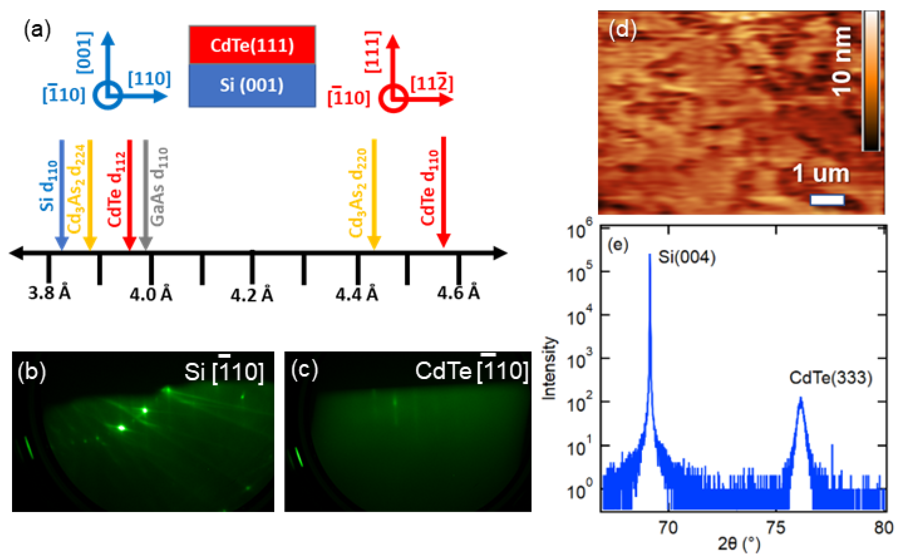
Figure 1a summarizes the relationship between the atomic spacing within the relevant layers and orientations. In particular, rotation of the crystallographic orientation reduces the mismatch between the CdTe layer from >10% to <1% in the case of GaAs by rotating the crystal to align the [110] and [11] axis. Attempts at using a ZnTe(001) as an interlayer analogous to GaAs(111) buffer structures would be possible but would require optimal growth conditions and microns of material to achieve high quality material [27]. Additionally, this would ultimately result in CdAs(001), which is a much higher energy surface [7]. High quality growth of CdTe(111) directly on GaAs(001) was previously achieved by engineering the interfacial chemistry to promote a strain-driven change in the crystallographic orientation [17,28,29]. That approach critically relies on maximizing Ga-Te bonding at the interface, namely a high temperature anneal combined with a Te pre-growth exposure, to create a pseudoepitaxial relationship with the (111) surface [30].
Although interfacial engineering is more limited with an elemental semiconductor, an analogous approach was also shown to work for Si [31] and is employed here. Following desorption of the surface oxide at high temperatures, as evident in the reflection high energy electron diffraction (RHEED) pattern shown in Figure 1b, As and Te surfactants are used during cool down to create a favorable bonding arrangement for CdTe epitaxy in the (111) orientation with minimal anti-phase domains. As is supplied until approximately 450 C, and then Te is supplied. It has been suggested from X-ray photoelectron spectroscopy that Te-Si bonding is favorable, whereas Cd-Si bonds are not formed, and further postulated that allowing Te to diffuse to step edges is critical to creating highly oriented films [32]. Often a substrate miscut of multiple degrees is used for this purpose in order to intentionally create steps to suppress twin domains. In this system, however, larger miscuts were shown to decrease crystal quality and increase tilt between the two layers [31]. On-axis substrates generally have a miscut of up to 0.5 and provide the starting surface with some density of steps. Whereas a spotty RHEED pattern was present during the initial CdTe nucleation phase, further annealing under Te results in a streakier RHEED (Figure 1c) pattern and ultimately a surface roughness of approximately 1 nm, as observed in AFM (Figure 1d). XRD patterns show only peaks related to the substrate and CdTe(111), with a (333) rocking curve peak full-width half-max (FWHM) of 730 arcseconds for 100 nm thick CdTe layers. Although this FWHM value is larger than those reported for similar growths on GaAs(001) [17], previous reports of CdTe growth on Si required thicknesses of >1 μm to achieve superior FWHM values [31]. This increased thickness is likely due to the limited ability to tailor the interface. FWHM of 60 arcseconds on GaAs(001) and 140 arcseconds on Si(001) have been reported on optimized samples with thicknesses > 8 μm [32], however, that amount of material is likely prohibitive for many applications.
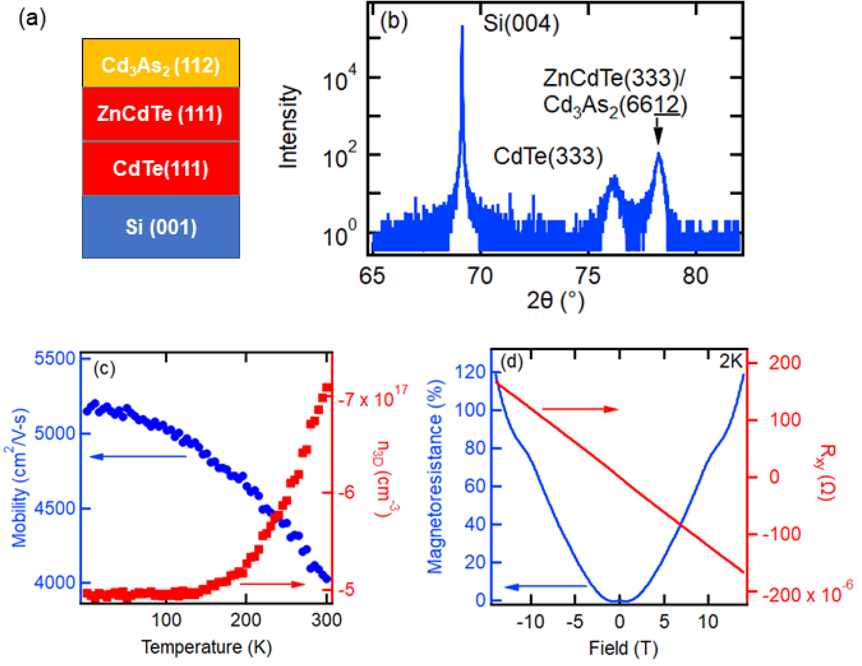
In order to obtain a two step buffer structure to establish a lattice-matched template for CdAs(112) growth, a ZnCdTe layer with approximately 42% Zn was grown atop the CdTe(111) nucleation layer, as shown in Figure 2a. The use of a lattice-matched buffer layer, even if only 100 nm thick, was shown to significantly enhance the mobility of similar structures on GaAs(111) substrates [26], and an analogous approach was shown to be effective on GaAs(001) [17]. Any attempts to introduce Zn into the initial nucleation layer resulted in both (111) and (001) related peaks visible in XRD patterns, highlighting the role of strain in this orientation change. Although no change in threading dislocation density was observed using electron channeling contrast imaging, evidence of other extended defects was observed in relaxed CdAs films that were not present in films grown on lattice-matched buffers. Studies in the (001) system showed minimal dependence on the threading dislocation density on the carrier mobilities of bulk thin films [20]. II–VI (111) and CdAs(112) related peaks are visible in the XRD pattern (CdAs has a 2:1 epitaxial relationship with II–VI layers). A resulting room temperature mobility of 4100 cm/V-s was measured and rose to 5200 cm/V-s at 2K. Carrier concentrations, as measured by the Hall voltage, decreased from 7.0 × 10 cm to 5.0 × 10 cm over that temperature range, slightly higher than typical values on GaAs substrates. These mobility values are similar to those measured in CdAs epilayers grown on on-axis ZnCdTe(111)/CdTe(111)/GaAs(001) [17] and ZnCdTe/GaAs(111) structures but below those grown on miscut GaAs(111) and GaAs(001) substrates to control for twin defects [26]. Magnetoresistance data taken at 2K looks typical of CdAs films, with a polynomial shape at lower fields that slowly transitions to a linear shape with increasing field. The main difference is that the transition to linear behavior occurs at a much larger field value and with a much lower overall magneoresistance amplitude due to the lower mobility. This linear behavior is a typical fingerprint of topological semimetal systems and has been theorized to arise due to a combination of small potential fluctuations due to disorder and a scattering time much larger than the cyclotron period [33]. Hall voltages were linear through at least 14T from 300K to 2K, indicating the transport is dominated by a single electron carrier.
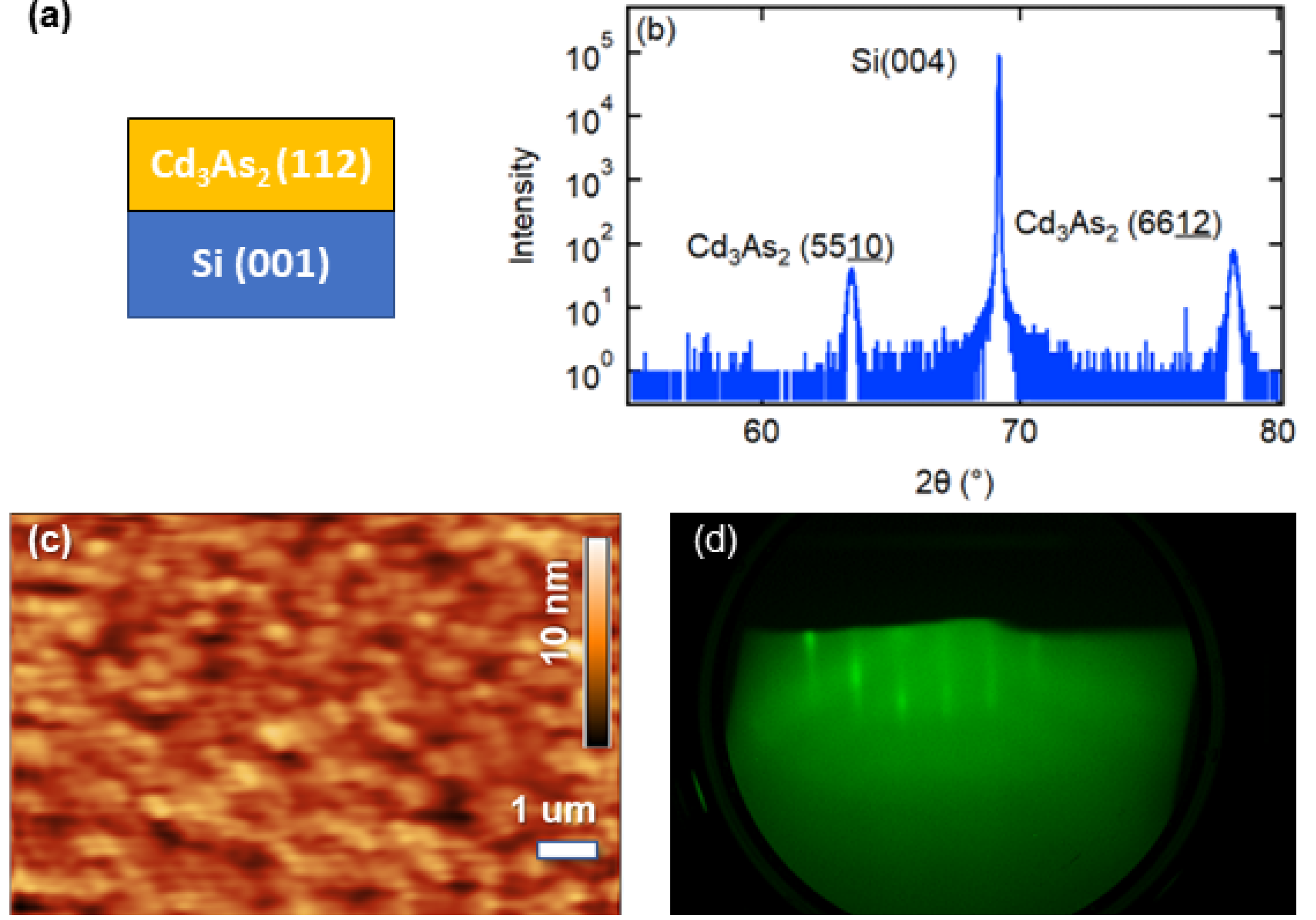
Finally, in an attempt to directly integrate CdAs with Si, the II–VI buffer layers were omitted, and CdAs growth was initiated immediately following cool down from the high temperature Si oxide desorption step under identical As/Te exposures, followed by an As exposure directly prior to growth. The direct CdAs nucleation occurred at similar temperatures as on II–VI buffer layers (100–115 C), but exhibited hazy, spotty RHEED patterns for a much longer period of time. AFM images, shown in Figure 3b, reveal a rougher (approximately 4 nm) surface morphology than typical (112) layers. Peaks related to CdAs(112) were only visible in the XRD spectrum, with no evidence of any [001] domains. The switch from the [001] orientation of the substrate is likely due to the much higher energy of the CdAs(001) surface [26] combined with a similar surface bonding mechanism that reorients CdTe in the <111> direction. RHEED observed during growth reveals a pattern and surface reconstruction typical of CdAs [17], as well as a changing pattern with rotation, consistent with a film with in-plane epitaxial registry rather than a textured polycrystal. Electrical measurements are not possible on the film due to the use of p-type substrate in this particular case. However, similar growth attempts directly on GaAs(001) resulted in room temperature mobilities of approximately 2000 cm/V-s, approximately half of typical values of relaxed films grown on on-axis GaAs(111) substrates and CdTe/ZnTe buffer layers.
4. Discussion
Although the electron mobility of CdAs epilayers grown on lattice-mismatched buffers remains high relative to semiconductors with similar dislocation densities, it is still sensitive to the surface on which it is grown. Because conventional GaAs and Si substrates do not have the same lattice spacing as CdAs, buffer layers play an important role in aiding nucleation and minimizing dislocation formation in the CdAs epilayers. In cases where (001) substrate orientations are preferred for device design or manufacturing considerations, the ability to switch the orientation of CdAs to its preferred (112) surface, through growth on a buffer layer or directly on the substrate, is also beneficial, providing smoother surfaces and than if a (001) orientation was preserved throughout the structure. The decrease in lattice mismatch in one direction with this rotation also requires less buffer layer material to achieve crystalline quality in such a structure.
We note three important aspects that play a role in the growth of CdAs on Si(001). First, although an analogous crystallographic orientation rotation takes place, the lattice mismatch between Si and CdTe ([10] and [11], respectively) is much greater than that between GaAs and CdTe in the same directions (−3.3% vs. 0.7%). The 4-fold symmetry of the substrate also opens the possibility of anti-phase domain formation. Both establish the potential for enhanced extended defect generation in the CdAs epilayers than growth on GaAs. Second, growths here were performed on on-axis Si(001) substrates. From previous growth efforts on GaAs(111) and (001) substrates, it is well known that twin domains can easily form in both the CdAs and the underlying II–VI buffer layers and can significantly limit the electron mobility. This point is highlighted by the fact that, despite the larger lattice mismatch, the room temperature mobility reported here for growth on Si(001) is on the lower end of what was reported for on-axis GaAs(111) (4000–6000 cm/V-S) [26]. Growth on miscut substrates helps to reduce twin domains, and for applications where these substrates are acceptable, much larger mobilities are likely achievable, even if the CdTe buffers may decrease slightly in crystalline quality from this [31]. Finally, it is possible that the epitaxial registry between the CdAs/Si is much weaker than on CdTe/Si structures, but because (112) is a much lower energy surface, minimizing this surface energy is largely driving the orientation shift in the case of growth directly on Si rather than the interfacial bonding and strain. No evidence is observed that these films are textured polycrystals, but pervasive, smaller scale in-plane misorientations are possible and more likely than when the growth structures contain buffer layers.
Growth of CdAs directly on Si offers an epitaxial route for applications where buffer layers would hinder vertical device performance or their incorporation is not possible while also providing the simplest growth approach possible. Deposition temperatures of only 100–150 C are compatible with most structures and would allow for CdAs films to be added late in the device fabrication process if combined with appropriate surface cleaning prior to growth. For structures that can withstand higher temperatures and require higher material quality, films may be annealed at temperatures well above 150 C. As noted earlier, the epitaxial registry may be quite weak, leading to in-plane disorder, and previous reports consistently show the limitations that extended defects put on the electron mobility. Starting from amorphous films, an annealing approach was shown to greatly improve crystal quality with short 500–600 C exposures (5 min) on SrTiO (001) [34] and led to mobilities above 30,000 cm/V-s. The high vapor pressure of CdAs requires thin films to be encapsulated to survive such high temperatures, such as using low-temperature atomic layer deposition of AlO, or SiN/SiO deposited on CdTe capped samples. Given the starting level of crystallinity in these thin films, similar levels of improvement should be possible.
Expanding the material selection to Weyl semimetals using similar approaches may also be possible to further expand possible applications. TaAs has recently been grown in thin film form on GaAs(001) as both a thin single crystal [35] and a polycrystal [5]. Beyond the previously discussed properties of chiral topological semimetals, the use of Weyl semimetals as an interconnect material is also promising due to their unique conductivity scaling with dimensionality [23], which, unlike conventional metals such as copper, does not increase with decreasing length scales because of its surface states. Growth of materials such as TaAs and NbAs will be more difficult due to higher synthesis temperatures (>350 C) and the possibility of interfacial silicide formation. CdAs can alternatively be magnetically doped to form a Weyl semimetal but would face additional growth challenges [36].
5. Conclusions
This work details two routes to epitaxially integrating CdAs onto Si(001) using both II–VI buffers and direct growth onto the substrate. These synthesis routes build on previous approaches for growth on compound semiconductors but tailor them for Si, significantly extending the technological uses of a topological semimetal. The combination of these strategies allow for a variety of device designs, and the low temperature growth process is compatible with a variety of existing Si device processing requirements. Although the electron mobility is lower than in CdAs films grown under optimized conditions on GaAs(111) or (001) substrates, we outline several additional approaches to realizing future improvement depending on the parameters and restrictions of the application. Ultimately, integration of Dirac and Weyl semimetals with Si(001) substrates expands the possibilities for (opto)electronic device design and performance beyond what is currently possible in integrated multiferroic oxides or direct-band gap compound semiconductors, or even conventional metallic interconnects. This study establishes a foundation for future integration advances of these systems.
Author Contributions
Conceptualization, A.R. and K.A.; methodology, A.R. and K.A.; investigation, K.A.; resources, A.R.; data curation, A.R.; writing—original draft preparation, A.R. and K.A.; writing—review and editing, A.R. and K.A.; supervision, K.A.; project administration, K.A.; funding acquisition, K.A. All authors have read and agreed to the published version of the manuscript.
Funding
This work was authored in part by employees of the Alliance for Sustainable Energy, LLC, the Manager and Operator of the National Renewable Energy Laboratory for the US Department of Energy (DOE) under Contract No. DE- AC36-08GO28308. Funding was provided by the Laboratory Directed Research and Development program.
Data Availability Statement
The data presented in this study are available on request from the corresponding author.
Acknowledgments
The authors want to thank Vincenzo LaSalvia for assistance in preparing Si substrates and Jocienne Nelson for assistance with electrical measurements. The views expressed in the article do not necessarily represent the views of the DOE or the U.S. Government. The U.S. Government retains and the publisher, by accepting the article for publication, acknowledges that the U.S. Government retains a nonexclusive, paid-up, irrevocable, worldwide license to publish or reproduce the published form of this work, or allow others to do so, for U.S. Government purposes.
Conflicts of Interest
The authors declare no conflict of interest.
Sample Availability
Samples of the compounds are available from the authors.
Abbreviations
The following abbreviations are used in this manuscript:
| MBE | Molecular beam epitaxy |
| RHEED | Reflection high enery electron diffraction |
| AFM | Atomic force microscopy |
| XRD | X-ray diffraction |
| FWHM | Full-width half-max |
References
- Liang, T.; Gibson, Q.; Ali, M.N.; Liu, M.; Cava, R.J.; Ong, N.P. Ultrahigh mobility and giant magnetoresistance in the Dirac semimetal Cd3As2. Nat. Mater. 2015, 14, 280–284. [Google Scholar] [CrossRef] [PubMed] [Green Version]
- Wang, Q.; Li, C.Z.; Ge, S.; Li, J.G.; Lu, W.; Lai, J.; Liu, X.; Ma, J.; Yu, D.P.; Liao, Z.M.; et al. Ultrafast Broadband Photodetectors Based on Three-Dimensional Dirac Semimetal Cd3As2. Nano Lett. 2017, 17, 834–841. [Google Scholar] [CrossRef] [PubMed] [Green Version]
- Spitzer, D.P.; Castellion, G.A.; Haacke, G. Anomalous Thermal Conductivity of Cd3As2 and the Cd3As2-Zn3As2 Alloys. J. Appl. Phys. 1966, 37, 3795–3801. [Google Scholar] [CrossRef]
- Yan, B.; Felser, C. Topological Materials: Weyl Semimetals. Annu. Rev. Condens. Matter Phys. 2017, 8, 337–354. [Google Scholar] [CrossRef] [Green Version]
- Yanez, W.; Ou, Y.; Xiao, R.; Koo, J.; Held, J.T.; Ghosh, S.; Rable, J.; Pillsbury, T.; Delgado, E.G.; Yang, K.; et al. Spin and Charge Interconversion in Dirac-Semimetal Thin Films. Phys. Rev. Appl. 2021, 16, 054031. [Google Scholar] [CrossRef]
- Yang, Y.; Xiu, F. Broadband Photodetection of Cd3As2: Review and Perspectives. Mater. Today Electron. 2022, 2, 100007. [Google Scholar] [CrossRef]
- Rice, A.D.; Lee, C.H.; Fluegel, B.; Norman, A.G.; Nelson, J.N.; Jiang, C.S.; Steger, M.; McGott, D.L.; Walker, P.; Alberi, K. Epitaxial Dirac Semimetal Vertical Heterostructures for Advanced Device Architectures. Adv. Funct. Mater. 2022, 32, 2111470. [Google Scholar] [CrossRef]
- Zhu, C.; Wang, F.; Meng, Y.; Yuan, X.; Xiu, F.; Luo, H.; Wang, Y.; Li, J.; Lv, X.; He, L.; et al. A robust and tuneable mid-infrared optical switch enabled by bulk Dirac fermions. Nat. Commun. 2022, 8, 14111. [Google Scholar] [CrossRef] [Green Version]
- Zhou, T.; Zhang, C.; Zhang, H.; Xiu, F.; Yang, Z. Enhanced thermoelectric properties of the Dirac semimetal Cd3As2. Inorg. Chem. Front. 2016, 3, 1637–1643. [Google Scholar] [CrossRef] [Green Version]
- Fu, C.; Sun, Y.; Felser, C. Topological thermoelectrics. APL Mater. 2020, 8, 040913. [Google Scholar] [CrossRef]
- Wang, H.; Luo, X.; Chen, W.; Wang, N.; Lei, B.; Meng, F.; Shang, C.; Ma, L.; Wu, T.; Dai, X.; et al. Magnetic-field enhanced high-thermoelectric performance in topological Dirac semimetal Cd3As2 crystal. Sci. Bull. 2018, 63, 411–418. [Google Scholar] [CrossRef] [Green Version]
- Rajamathi, C.R.; Gupta, U.; Kumar, N.; Yang, H.; Sun, Y.; Süß, V.; Shekhar, C.; Schmidt, M.; Blumtritt, H.; Werner, P.; et al. Weyl Semimetals as Hydrogen Evolution Catalysts. Adv. Mater. 2017, 29, 1606202. [Google Scholar] [CrossRef]
- Crassee, I.; Sankar, R.; Lee, W.L.; Akrap, A.; Orlita, M. 3D Dirac semimetal Cd3As2: A review of material properties. Phys. Rev. Mater. 2018, 2, 120302. [Google Scholar] [CrossRef] [Green Version]
- Ali, M.N.; Gibson, Q.; Jeon, S.; Zhou, B.B.; Yazdani, A.; Cava, R.J. The Crystal and Electronic Structures of Cd3As2, the Three-Dimensional Electronic Analogue of Graphene. Inorg. Chem. 2014, 53, 4062–4067. [Google Scholar] [CrossRef] [Green Version]
- Schumann, T.; Goyal, M.; Kim, H.; Stemmer, S. Molecular beam epitaxy of Cd3As2 on a III–V substrate. APL Mater. 2016, 4, 126110. [Google Scholar] [CrossRef] [Green Version]
- Kealhofer, D.A.; Kim, H.; Schumann, T.; Goyal, M.; Galletti, L.; Stemmer, S. Basal-plane growth of cadmium arsenide by molecular beam epitaxy. Phys. Rev. Mater. 2019, 3, 031201. [Google Scholar] [CrossRef]
- Rice, A.D.; Nelson, J.; Norman, A.G.; Walker, P.; Alberi, K. High Mobility Cd3As2(112) on GaAs(001) Substrates Grown via Molecular Beam Epitaxy. ACS Appl. Electron. Mater. 2022, 4, 729–734. [Google Scholar] [CrossRef]
- Warren, E.L.; Kibbler, A.E.; France, R.M.; Norman, A.G.; Stradins, P.; McMahon, W.E. Growth of antiphase-domain-free GaP on Si substrates by metalorganic chemical vapor deposition using an in situ AsH3 surface preparation. Appl. Phys. Lett. 2015, 107, 082109. [Google Scholar] [CrossRef]
- Liu, A.Y.; Srinivasan, S.; Norman, J.; Gossard, A.C.; Bowers, J.E. Quantum dot lasers for silicon photonics [Invited]. Photonics Res. 2015, 3, B1–B9. [Google Scholar] [CrossRef] [Green Version]
- Goyal, M.; Salmani-Rezaie, S.; Pardue, T.N.; Guo, B.; Kealhofer, D.A.; Stemmer, S. Carrier mobilities of (001) cadmium arsenide films. APL Mater. 2020, 8, 051106. [Google Scholar] [CrossRef]
- Osterhoudt, G.B.; Diebel, L.K.; Gray, M.J.; Yang, X.; Stanco, J.; Huang, X.; Shen, B.; Ni, N.; Moll, P.J.W.; Ran, Y.; et al. Colossal mid-infrared bulk photovoltaic effect in a type-I Weyl semimetal. Nat. Mater. 2019, 18, 471–475. [Google Scholar] [CrossRef] [PubMed]
- Rees, D.; Manna, K.; Lu, B.; Morimoto, T.; Borrmann, H.; Felser, C.; Moore, J.E.; Torchinsky, D.H.; Orenstein, J. Helicity-dependent photocurrents in the chiral Weyl semimetal RhSi. Sci. Adv. 2020, 6, eaba0509. [Google Scholar] [CrossRef] [PubMed]
- Chen, C.T.; Bajpai, U.; Lanzillo, N.A.; Hsu, C.H.; Lin, H.; Liang, G. Topological Semimetals for Scaled Back-End-Of-Line Interconnect Beyond Cu. In Proceedings of the 2020 IEEE International Electron Devices Meeting (IEDM), San Francisco, CA, USA, 12–18 December 2020; pp. 32.4.1–32.4.4. [Google Scholar] [CrossRef]
- Zhang, C.; Ni, Z.; Zhang, J.; Yuan, X.; Liu, Y.; Zou, Y.; Liao, Z.; Du, Y.; Narayan, A.; Zhang, H.; et al. Ultrahigh conductivity in Weyl semimetal NbAs nanobelts. Nat. Mater. 2019, 18, 482–488. [Google Scholar] [CrossRef] [PubMed]
- Kern, W.; Puotinen, D.A. Cleaning Solutions Based on Hydrogen Peroxide for Use in Silicon Semiconductor Technology. RCA Rev. 1970, 31, 21. [Google Scholar]
- Rice, A.D.; Park, K.; Hughes, E.T.; Mukherjee, K.; Alberi, K. Defects in Cd3As2 epilayers via molecular beam epitaxy and strategies for reducing them. Phys. Rev. Mater. 2019, 3, 121201. [Google Scholar] [CrossRef] [Green Version]
- Chen, Y.; Simingalam, S.; Brill, G.; Wijewarnasuriya, P.; Dhar, N.; Kim, J.J.; Smith, D.J. MBE-Grown ZnTe/Si, a Low-Cost Composite Substrate. J. Electron. Mater. 2012, 41, 2917–2924. [Google Scholar] [CrossRef]
- Ballingall, J.; Takei, W.; Feldman, B.J. Low defect density CdTe(111)-GaAs(001) heterostructures by molecular beam epitaxy. Appl. Phys. Lett. 1985, 47, 599–601. [Google Scholar] [CrossRef]
- Ballingall, J.; Wroge, M.; Leopold, D. (100) and (111) oriented CdTe grown on (100) oriented GaAs by molecular beam epitaxy. Appl. Phys. Lett. 1986, 48, 1273–1275. [Google Scholar] [CrossRef]
- Bourret, A.; Fuoss, P.; Feuillet, G.; Tatarenko, S. Solving an interface structure by electron microscopy and x-ray diffraction: The GaAs(001)-CdTe(111) interface. Phys. Rev. Lett. 1993, 70, 311. [Google Scholar] [CrossRef]
- Chen, Y.P.; Sivananthan, S.; Faurie, J.P. Structure of CdTe(111)B grown by MBE on misoriented Si(001). J. Electron. Mater. 1993, 60, 951–959. [Google Scholar] [CrossRef]
- Faurie, J.; Sporken, R.; Chen, Y.; Lange, M.; Sivananthan, S. Heteroepitaxy of CdTe on GaAs and silicon substrates. Mater. Sci. Eng. B 1993, 16, 51–56. [Google Scholar] [CrossRef]
- Song, J.C.W.; Refael, G.; Lee, P.A. Linear magnetoresistance in metals: Guiding center diffusion in a smooth random potential. Phys. Rev. B 2015, 92, 180204. [Google Scholar] [CrossRef] [Green Version]
- Nakazawa, Y.; Uchida, M.; Nishihaya, S.; Kriener, M.; Kozuka, Y.; Taguchi, Y.; Kawasaki, M. Structural characterisation of high-mobility Cd3As2 films crystallised on SrTiO3. Sci. Rep. 2018, 8, 2244. [Google Scholar] [CrossRef] [Green Version]
- Sadowski, J.; Domagała, J.Z.; Zajkowska, W.; Kret, S.; Seredyński, B.; Gryglas-Borysiewicz, M.; Ogorzałek, Z.; Bożek, R.; Pacuski, W. Structural properties of TaAs Weyl semimetal thin films grown by molecular beam epitaxy on GaAs(001) substrates. Cryst. Growth Des. 2022, 22, 6039–6045. [Google Scholar] [CrossRef]
- Xiao, R.; Held, J.T.; Rable, J.; Ghosh, S.; Wang, K.; Mkhoyan, K.A.; Samarth, N. Challenges to magnetic doping of thin films of the Dirac semimetal Cd3As2. Phys. Rev. Mater. 2022, 6, 024203. [Google Scholar] [CrossRef]
Figure 1.
Summary of CdTe(111) growth on Si(001): (a) layer schematic of data shown in (b–d) along with crystallographic orientation of the major axis of Si (blue) and CdTe (red) as well as a plot of atomic spacing of Si, GaAs in the <110> direction, and CdTe, CdAs in [110], [220] and [11], [22] directions, respectively. CdAs has a 2:1 epitaxial relationship with the semiconductor layers; (b) RHEED image of Si(001) following oxide desorption; (c) RHEED image of CdTe(111) following anneal; (d) AFM image of CdTe(111) surface; (e) XRD of CdTe(111) grown directly on Si(001).

Figure 2.
Growth of CdAs on CdTe(111)/Si(001): (a) layer schematic of sample shown in (b–d); (b) XRD pattern of CdAs grown on a two step II–VI buffer on Si(001); (c) temperature dependent Hall data showing carrier concentration (right axis) and mobility (left axis); (d) magnetoresistance (left axis) and (right axis) as a function of magnetic field taken at 2K.

Figure 3.
Demonstration of direct growth of CdAs on Si(001): (a) layer schematic; (b) AFM image of CdAs grown directly on Si(001); (c) XRD pattern of Cd3As2/Si(001) showing only (112) related peaks; (d) RHEED pattern of CdAs surface.
Figure 3.
Demonstration of direct growth of CdAs on Si(001): (a) layer schematic; (b) AFM image of CdAs grown directly on Si(001); (c) XRD pattern of Cd3As2/Si(001) showing only (112) related peaks; (d) RHEED pattern of CdAs surface.

Disclaimer/Publisher’s Note: The statements, opinions and data contained in all publications are solely those of the individual author(s) and contributor(s) and not of MDPI and/or the editor(s). MDPI and/or the editor(s) disclaim responsibility for any injury to people or property resulting from any ideas, methods, instructions or products referred to in the content. |
© 2023 by the authors. Licensee MDPI, Basel, Switzerland. This article is an open access article distributed under the terms and conditions of the Creative Commons Attribution (CC BY) license (https://creativecommons.org/licenses/by/4.0/).
Share and Cite
MDPI and ACS Style
Rice, A.; Alberi, K. Epitaxial Integration of Dirac Semimetals with Si(001). Crystals 2023, 13, 578. https://doi.org/10.3390/cryst13040578
AMA Style
Rice A, Alberi K. Epitaxial Integration of Dirac Semimetals with Si(001). Crystals. 2023; 13(4):578. https://doi.org/10.3390/cryst13040578
Chicago/Turabian StyleRice, Anthony, and Kirstin Alberi. 2023. "Epitaxial Integration of Dirac Semimetals with Si(001)" Crystals 13, no. 4: 578. https://doi.org/10.3390/cryst13040578
Note that from the first issue of 2016, this journal uses article numbers instead of page numbers. See further details here.