Article

Molecular Beam Epitaxy of Twin-Free Bi2Se3 and Sb2Te3 on In2Se3/InP(111)B Virtual Substrates

by
Kaushini S. Wickramasinghe
1,
Candice Forrester
1,2 and
Maria C. Tamargo
1,2,*
1
Department of Chemistry, The City College of New York, New York, NY 10031, USA
2
Chemistry Program, CUNY Graduate Center, New York, NY 10016, USA
*
Author to whom correspondence should be addressed.
Crystals 2023, 13(4), 677; https://doi.org/10.3390/cryst13040677
Submission received: 17 March 2023 / Revised: 7 April 2023 / Accepted: 12 April 2023 / Published: 14 April 2023
(This article belongs to the Special Issue Epitaxial Growth of Semiconductor Materials and Devices)

Abstract

:
Three-dimensional topological insulators (3D-TIs) are a new generation of materials with insulating bulk and exotic metallic surface states that facilitate a wide variety of ground-breaking applications. However, utilization of the surface channels is often hampered by the presence of crystal defects, such as antisites, vacancies, and twin domains. For terahertz device applications, twinning is shown to be highly deleterious. Previous attempts to reduce twins using technologically important InP(111) substrates have been promising, but have failed to completely suppress twin domains while preserving high structural quality. Here we report growth of twin-free molecular beam epitaxial Bi2Se3 and Sb2Te3 structures on ultra-thin In2Se3 layers formed by a novel selenium passivation technique during the oxide desorption of smooth, non-vicinal InP(111)B substrates, without the use of an indium source. The formation of un-twinned In2Se3 provides a favorable template to fully suppress twin domains in 3D-TIs, greatly broadening novel device applications in the terahertz regime.

1. Introduction

Three dimensional topological insulators (3D-TIs) have attracted a great deal of interest in the past decade due to their non-trivial topology, which gives rise to metallic surface states protected by time reversal symmetry, and an insulating bulk [1,2,3,4]. A wide variety of applications in thermoelectrics [5], spintronics [6], twistronics [7,8], and quantum computation [9,10] are being considered. They also provide a fundamental platform to explore novel physics [11]. The topological nature of the surface states also enables a range of other novel technologies such as polarization selective terahertz detectors [12,13,14]. In these, the single-crystal nature of the TIs becomes of paramount importance.
Among the 3D-TIs, Bi2Se3 and Sb2Te3 are most actively pursued due to their experimentally verified single Dirac cone at the Γ point [15]. Their crystal structure is rhombohedral with a space group, D 3 d 5 ( R 3 ¯ m ) , with one formula unit (five atoms) per unit cell [2]. They are layered materials that exhibit a quintuple layer (QL) structure consisting of Se-Bi-Se-Bi-Se atoms along the c-direction. The QLs are separated by a van der Waals gap. Because of their van der Waals nature, there is a wide range of substrates that can be used for the epitaxial growth of these TIs [16,17,18].
However, the influence of the substrate on the molecular beam epitaxy (MBE)-grown material properties has been shown to be non-negligible [19,20]. It has been shown that, in some cases, there is a chemical interaction between the atoms of the substrate and the material at the interface which gives rise to quasi van der Waals growth [19,20] or, other times, an amorphous disordered interfacial layer is present [21]. Furthermore, there is a large unintentional background doping that conceals their surface channels [16,21], mainly due to the above mentioned interface issue, as well as to the inherent low-energy native defects [22] (Se or Te vacancies and antisite defects). Thus, the device and transport studies of these materials have been hindered [16,23]. Many efforts to reduce background doping have been reported; for example, improving the interface via different substrate preparation techniques [24,25] and growing a buffer layer of In2Se3 [25] or InxBi1−xSe3 [26,27] have shown a significant reduction in defects and background doping in Bi2Se3.
Moreover, crystal defects such as twin domains [28,29] are frequently observed regardless of the substrate or the buffer layer that is being used. In some applications, twinning in these layers is shown to be more deleterious to topological properties than intrinsic bulk doping. For example, twinning reduces helicity dependent topological photocurrent; thus, eliminating twinning can provide a path to chip-scale polarimeters [14], among other devices.
Most often, the 3D-TIs are grown on sapphire substrates due to sapphire’s low cost and inert chemical nature. InP(111), a substrate of considerable technological importance, and its surface provide the appropriate symmetry and lattice constant for Bi2Se3 growth, and thus may offer advantages over sapphire as a substrate. InP(111) has been used before and reported by some to produce good material properties [28,30,31], although with twin domains. There are a few reports of full twin suppression of Bi2Se3 by growing on 3.5° off-cut InP(111)A [19], rough InP(111)A [19], InP(115) [32], and rough InP(111)B [33] substrates. In the first two studies mentioned here, there is little information reported on the details of the structural analysis of the quality of the layers. In the case of InP(115) [32], a giant corrugation of the layers resulted in low structural quality and high strain, which even modified the band structure of Bi2Se3. In the study of rough InP(111)B [33], in which a detailed structural analysis was done, a lower quality of Bi2Se3 was obtained compared to the previously reported high quality, twinned Bi2Se3 on smooth InP(111)B [31], as indicated by the broadening of the full width at half maximum (FWHM) of the rocking curve on rough substrates. Therefore, there is a critical need to improve the quality of these twin-suppressed layers.
Although structurally InP(111)B is almost ideal for Bi2Se3 growth, the reactivity of the InP surface makes its preparation for growth more complex. As a method of compensating for the reactivity of Si(111) substrates, an In2Se3 [25] buffer was used, which improved the quality of the layer but did not help with twin suppression when grown on flat non-vicinal substrates. In2Se3 grown on Si(111) vicinal substrates [25] suppressed the twinning but gave rise to a corrugated surface. Therefore, the details of how we prepare the InP substrate before the growth of any layer are of utmost importance, and the influence of the substrate on the growth layer can be critical.
In this study we have investigated a novel method developed by us for the preparation of the non-vicinal InP(111)B substrate surface, and explored its properties with regard to formation of lower defect densities in the TI materials, in particular of twin domains. As the substrate preparation technique, we developed a new method that results in the formation of 2-dimentional (2D) van der Waals In2Se3 ultra-thin layers via Se passivation during the oxide desorption process of the smooth non-vicinal InP(111) substrate, in a molecular beam epitaxy (MBE) environment. The In2Se3 is formed without using an indium (In) source. With this new technique, we transformed the first few layers of the InP substrate into a van der Waals In2Se3 layer which is structurally and chemically compatible with Bi2Se3. Owing to this formation process, the resulting layers are fully twin suppressed.
It has previously been shown that growing single phase In2Se3 is very difficult, since In2Se3 has many different phases that can be formed readily [34]. Even when single phase In2Se3 was achieved, the layers were twinned [25,35]. Conventional MBE growth of In2Se3 would not produce un-twinned layers because there is freedom for the arriving indium atoms to move on the surface and form equally energetically favorable twin domains. One way to obtain twin-suppressed In2Se3 is to restrict the degrees of freedom of the indium atoms so that only one of the twin domains is favorable. Our approach, of forming the In2Se3 layer by an exchange of InP(111) P atoms with Se atoms, achieves this restriction, and leads to un-twinned In2Se3 layers, resulting in an ideal virtual substrate for the growth of Bi2Se3 and Sb2Te3. In this paper we present our surface modification technique and investigate the effect of this layer on the quality of epitaxial Bi2Se3 and Sb2Te3 grown on this virtual substrate. We present the growth details and the quality of the resulting In2Se3 and explore the crystal quality and twin-free nature of Bi2Se3 and Sb2Te3 layers grown on In2Se3/InP(111) virtual substrates by MBE.

2. Materials and Methods

All samples were grown on smooth non-vicinal Fe doped InP(111)B ± 0.5° substrates, which have a phosphorus-terminated surface. A Riber 2300P system with a base pressure of 5 × 10¹¹ Torr was used, equipped with in-situ reflection high-energy electron diffraction (RHEED) to monitor the growth of the material in real time. High-purity (99.9999%) bismuth (Bi) and antimony (Sb) fluxes were provided by a RIBER dual-zone effusion cell, a RIBER valved cracker cell was used for selenium (Se), and a single zone Knudsen cell for tellurium (Te). Beam equivalent pressure (BEP) was measured by an ultra-high vacuum (UHV) nude ion gauge placed in the path of the fluxes. All temperatures reported here were measured using thermocouple.

2.1. Formation of In2Se3 via Selenium Passivation of InP(111)B

The key to the nucleation of a twin-free In2Se3 layer on the InP substrate is the control of the nucleation process such that it avoids the coalescence of multiple nucleation sites into one continuous layer. Thus, the standard approach of deposition of In and Se atoms on the oxide-free InP surface does not work. The approach taken here is to use the In from the InP(111) surface. In this process, the In atoms act as fixed “anchors” that ensure the layer is all equally aligned. The following steps were used to form the In2Se3 layer. First, the substrate temperature (Tsub) was raised to 200 °C and held for 5 min to stabilize the temperature; at this point the RHEED pattern was completely spotty (1 × 1), as shown in Figure 1a. This is typical for an oxidized rough surface. A selenium overpressure of 1 × 10⁻⁵ Torr was provided at a substrate temperature of 300 °C and above, to prevent the out diffusion of phosphorus (P) atoms. Then, the temperature was raised gradually up to 495 °C at an average rate of 50 °C per minute without annealing at any temperature; at this point the RHEED pattern had changed to a mix of streaks and spots (Figure 1b), suggesting the onset of deoxidation. The substrate was annealed for 5 min at this temperature while observing the RHEED, which remained unchanged. After that, the temperature was increased to 505 °C and annealed for another 5 min. At this point the RHEED pattern became completely streaky (1 × 1) (Figure 1c), indicating full oxide removal from the surface. As soon as the RHEED pattern changed to a fully streaky pattern, the power to the substrate heater was shut down, allowing a rapid cool down to 190 °C. After the oxide removal, the streaky (1 × 1) RHEED pattern remained unchanged. This pattern corresponds to the surface reconstruction of the newly formed In2Se3 layer during the oxide desorption process, without using an external indium source.
Once the temperature reached 190 °C, in order to deposit an epitaxial layer on the In2Se3 surface, either the Se flux was adjusted to the required amount for Bi2Se3 growth or the Se shutter was closed for Sb2Te3 growth, and then the substrate temperature was raised to the required growth temperature. The temperature of the substrate was held at the growth temperature for 10 min before starting the growth to ensure a clean surface with no excess Se on the surface.

2.2. Growth of Bi2Se3 and Sb2Te3 on In2Se3/InP(111)B

A series of Bi2Se3 and Sb2Te3 samples were grown on an In2Se3 layer to optimize and investigate the structural and electrical properties of these materials. The Bi2Se3 growth temperature was varied in the range of Tsub = 245–295 °C while a fixed growth rate of ~0.5 nm/minute and a BEP ratio of Se to Bi ~100:1 were maintained. A 1 × 1 RHEED pattern was evident after Bi2Se3 growth with an enhanced streak intensity relative to the In2Se3 layer, as shown in Figure 2a. The Sb2Te3 growth temperature was varied in the range of Tsub = 235–260 °C with a growth rate ~0.25 nm/minute and a BEP ratio of Te to Sb ~15:1. The 1 × 1 RHEED pattern after Sb2Te3 growth is shown in Figure 2b. A layer of Sb2Te3 was also grown on a Bi2Se3 (18 nm) layer grown on the In2Se3 surface at a growth temperature of Tsub = 250 °C. BEP ratios of Se to Bi ~100:1 and Te to Sb ~15:1 were used. After growth of Sb2Te3/Bi2Se3, a 1 × 1 RHEED pattern was observed, as shown in Figure 2c. The post growth RHEED intensity in both cases of the Sb2Te3 growth decreased compared to the RHEED intensity of the In2Se3 layer. A summary of the samples presented in the study is given in Table 1.

2.3. Structural and Electrical Characterization

A Bruker D8 Discover diffractometer with a da Vinci configuration and a conditioned Cu Kα1(1.5418 Å) source was used for The XRD measurements. In the instrument, an intense beam of Cu Kα1 radiation is produced by passing the X-ray beam through a hybrid 2-bounce asymmetric Ge(220) monochromator (Bragg reflection angle is 22.6488°), which includes a Göbel Mirror. For high-resolution X-ray diffraction (HRXRD) rocking curve measurements, an additional Ge(220) analyzer crystal is used which limits the resolution of full width at half maximum (FWHM) of the rocking curve to 0.004°. XRD 2θ-ω scan, rocking curve (ω scan), and ϕ scan are used for the crystal analysis. In the 2θ-ω scan, the source moves so that ω is swept through a prescribed angle and the detector is rotated twice as fast as the source, while the sample is held at a fixed position. Rocking curve measurement, or the ω-scan, is performed by moving the source so that ω is swept through a prescribed angle while the sample and the detector are stationary. In the ϕ-scan, the sample is rotated around an axis normal to the surface of the sample. In this context ω is the angle between the sample and the source. The Bragg reflection angles (2θ) of (006) In2Se3 and (006) Bi2Se3 are 18.863° and 18.559°, respectively.
A Bruker Dimension FastScan AFM with a FastScan-A silicon probe was used to capture the atomic force microscopy (AFM) images. Surface roughness (root mean square roughness, Rq) of the samples was determined using 4µm2 AFM scans. Transport properties were measured in van der Pauw geometry using four-wire measurements in a closed-cycle helium cryostat at 10 K. Square pieces of ~5 mm × 5 mm were used for the measurement and the electrical contacts were made using pure indium.

3. Results and Discussion

This section is composed of three sub-sections. We discuss the structural properties of the In2Se3 layer. Subsequently, structural and transport properties of Bi2Se3 and Sb2Te3 layers are discussed in detail. The discussion includes comparisons of current results with previously reported results in the literature thereby emphasizing the significance of our work.

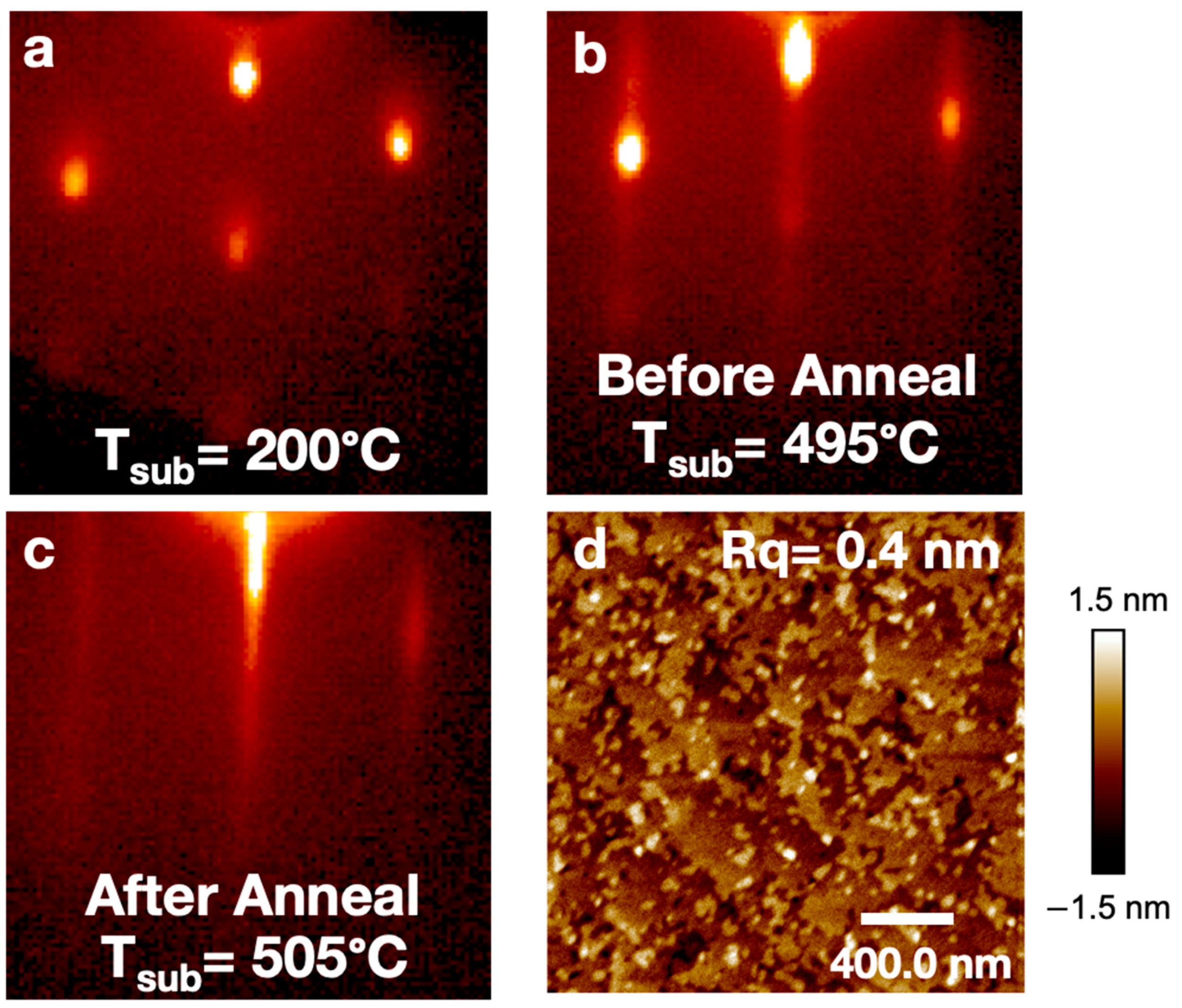
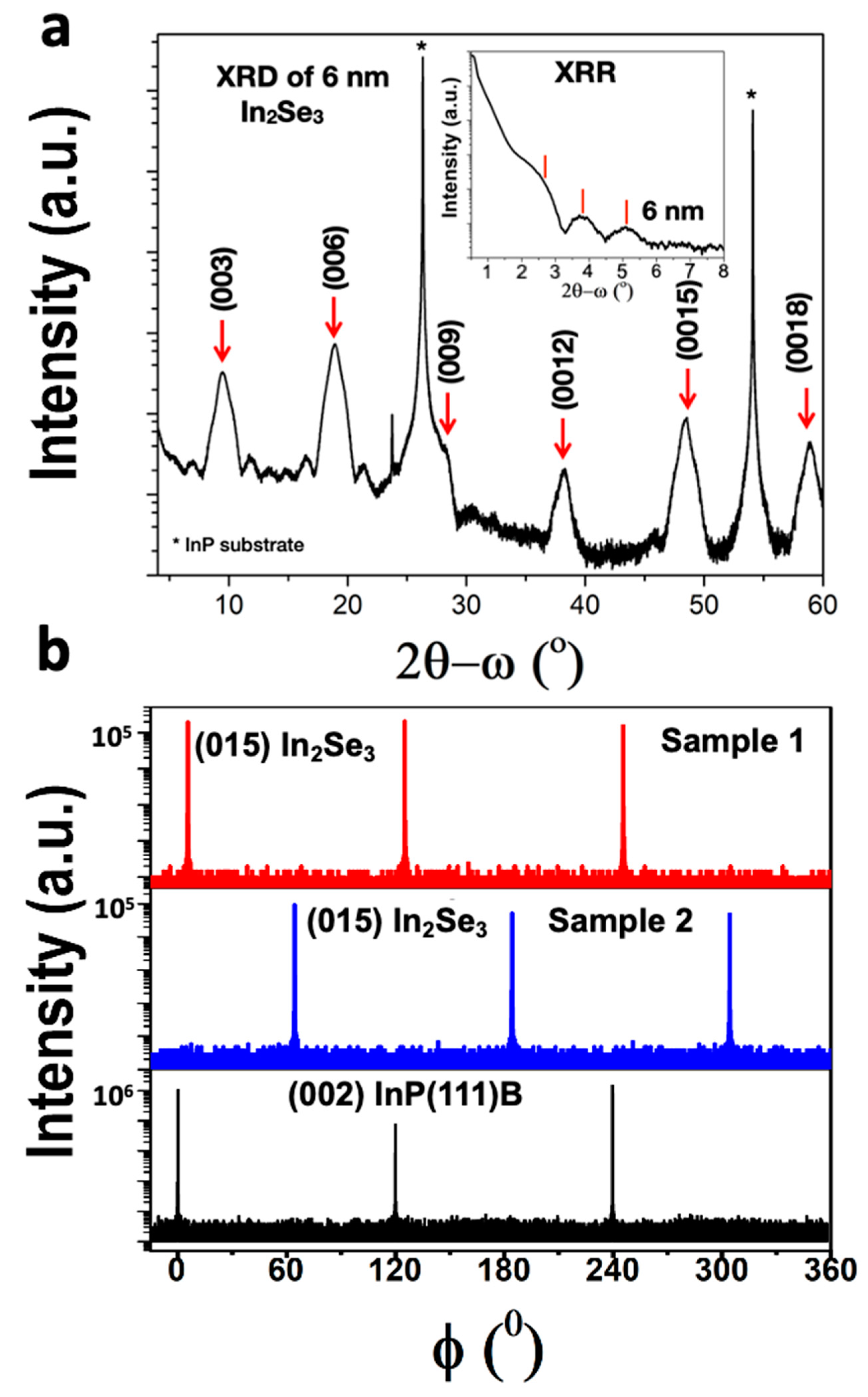
3.1. Structural Properties of In2Se3/InP(111)B Virtual Substrate

Figure 1d shows an atomic force microscopy (AFM) image of a smooth, atomically flat In2Se3 layer formed during Se passivation of the smooth non-vicinal InP(111)B substrate without an indium source. This layer has a roughness of Rq = 0.4 nm. The XRD 2θ-ω scan of the In2Se3 layer, which is shown in Figure 3a, has well-defined peaks from multiple reflections of (003) plane. The position of the peaks indicates that the sample is 3R In2Se3, a rhombohedral crystal structure; the data suggest it could be either α-In2Se3 (R3m) or β-In2Se3 ( R 3 ¯ m ) [36,37]. The high crystallinity of the In2Se3 layer is evidenced by the thickness fringes of the (006) reflection from which the thickness was calculated. The inset in Figure 3a is an X-ray reflectivity (XRR) scan of the In2Se3 layer presenting pronounced oscillations; the thickness calculated using these oscillations is comparable to the value obtained using the thickness fringes in the XRD 2θ-ω scan (thickness of ~6 nm). The full width at half maximum (FWHM) of the high-resolution X-ray diffraction (HRXRD) rocking curve is 0.06° (see Supplemental Information Figure S1a), which is a good number for an ultra-thin layer. Figure 3b shows the XRD ϕ scan of the (015) plane of two different In2Se3 samples with the characteristic three peaks, one peak at every 120°, indicating that the layer consists of a single domain. The FWHM of the XRD ϕ scan is 0.01°, which confirms that the hexagonal lattice of In2Se3 is aligned parallel to that of the InP(111) within a twist angle as small as 0.01° (see Supplemental Information Figure S2b). Figure 3b shows that the three peaks do not always occur at the same in-plane angle as the (200) plane reflections of the substrate; rather, in some cases, the 60° rotation of the In2Se3 layer relative to the interface of the substrate is preferred [28]. In both cases, the In2Se3 layer is un-twinned.

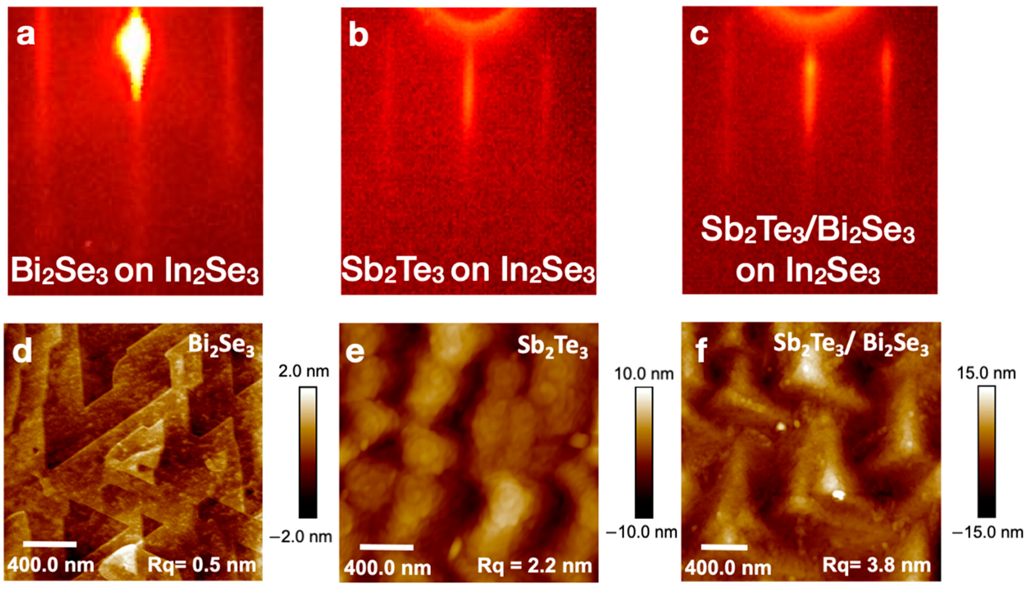
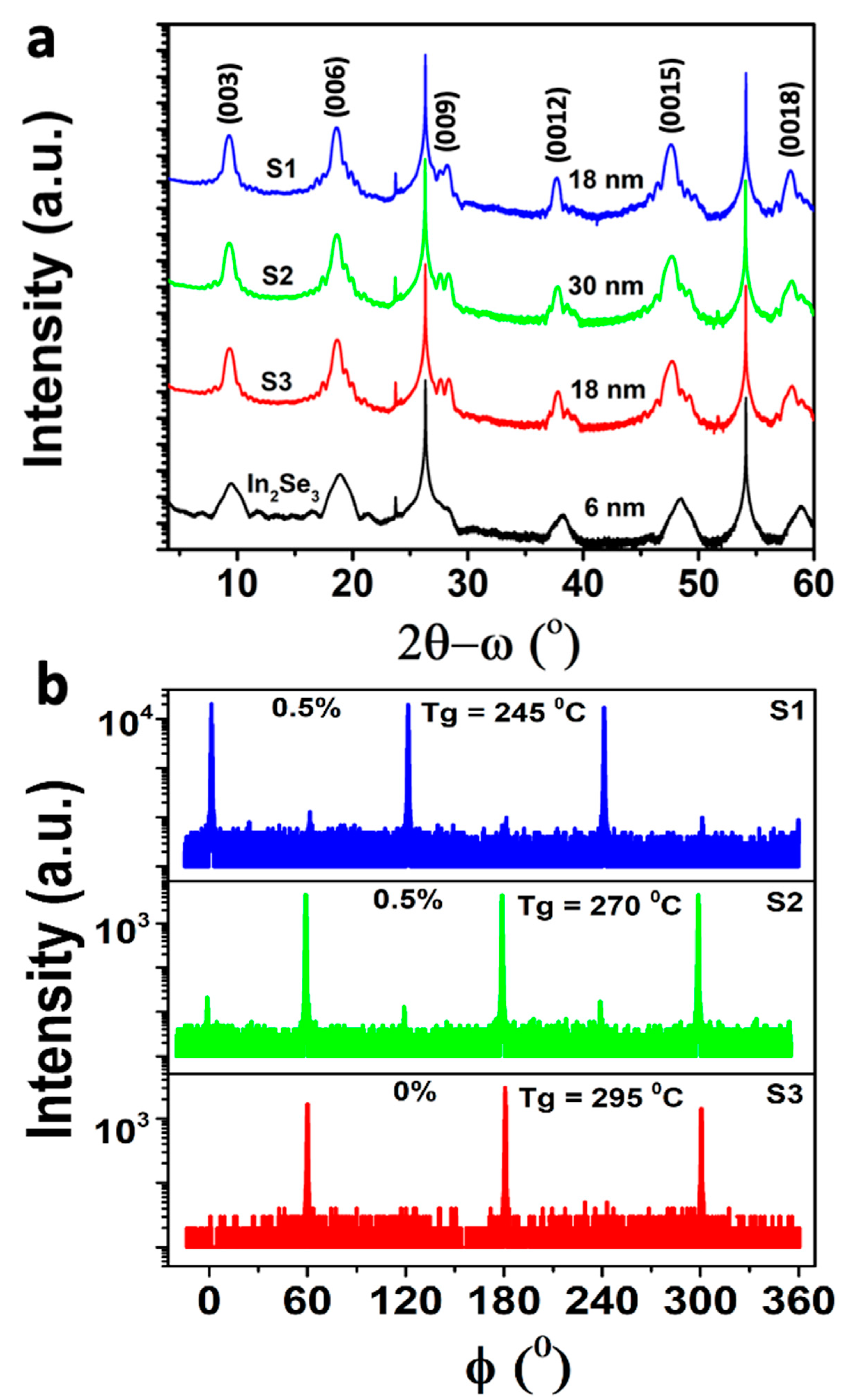
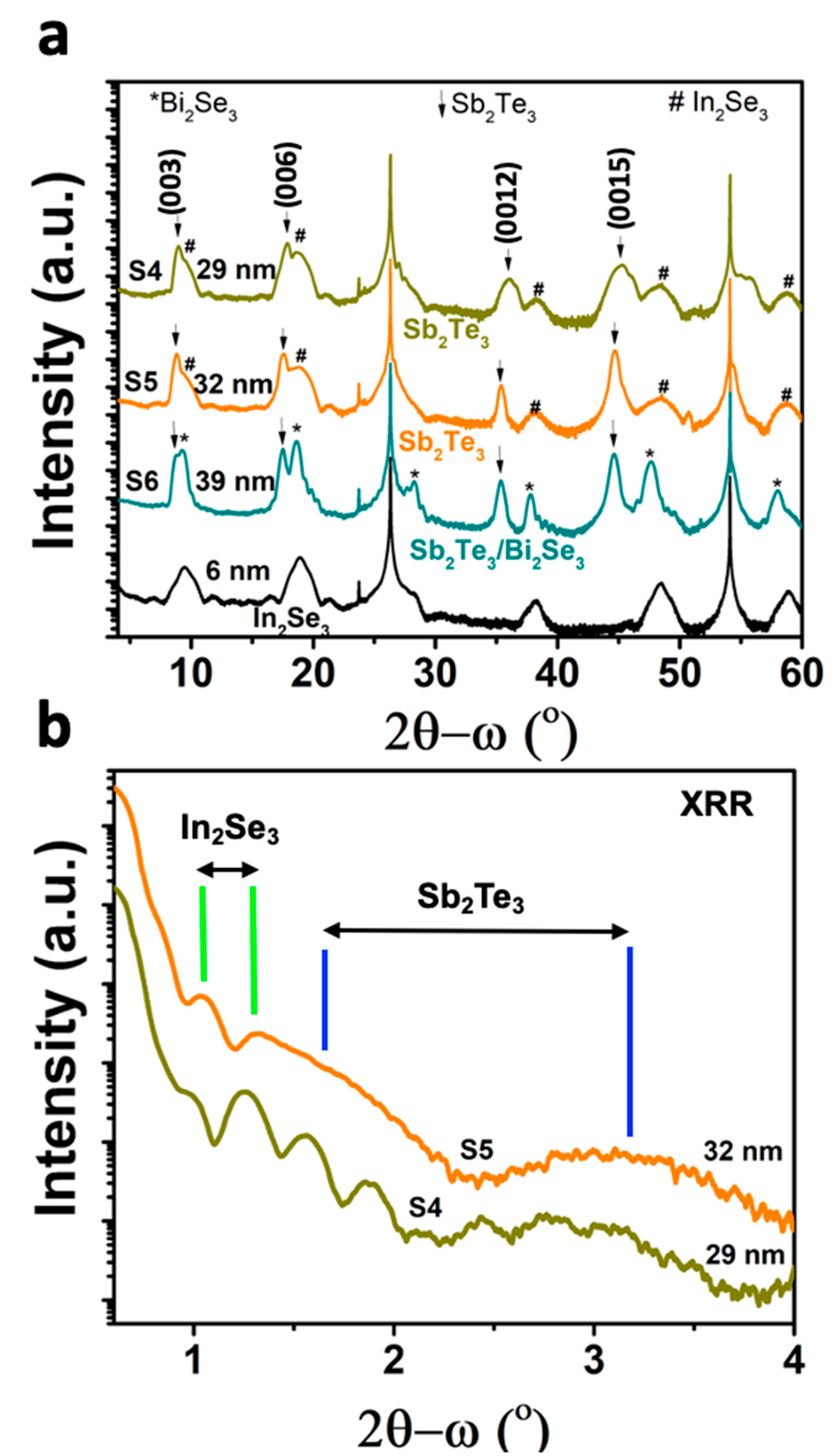
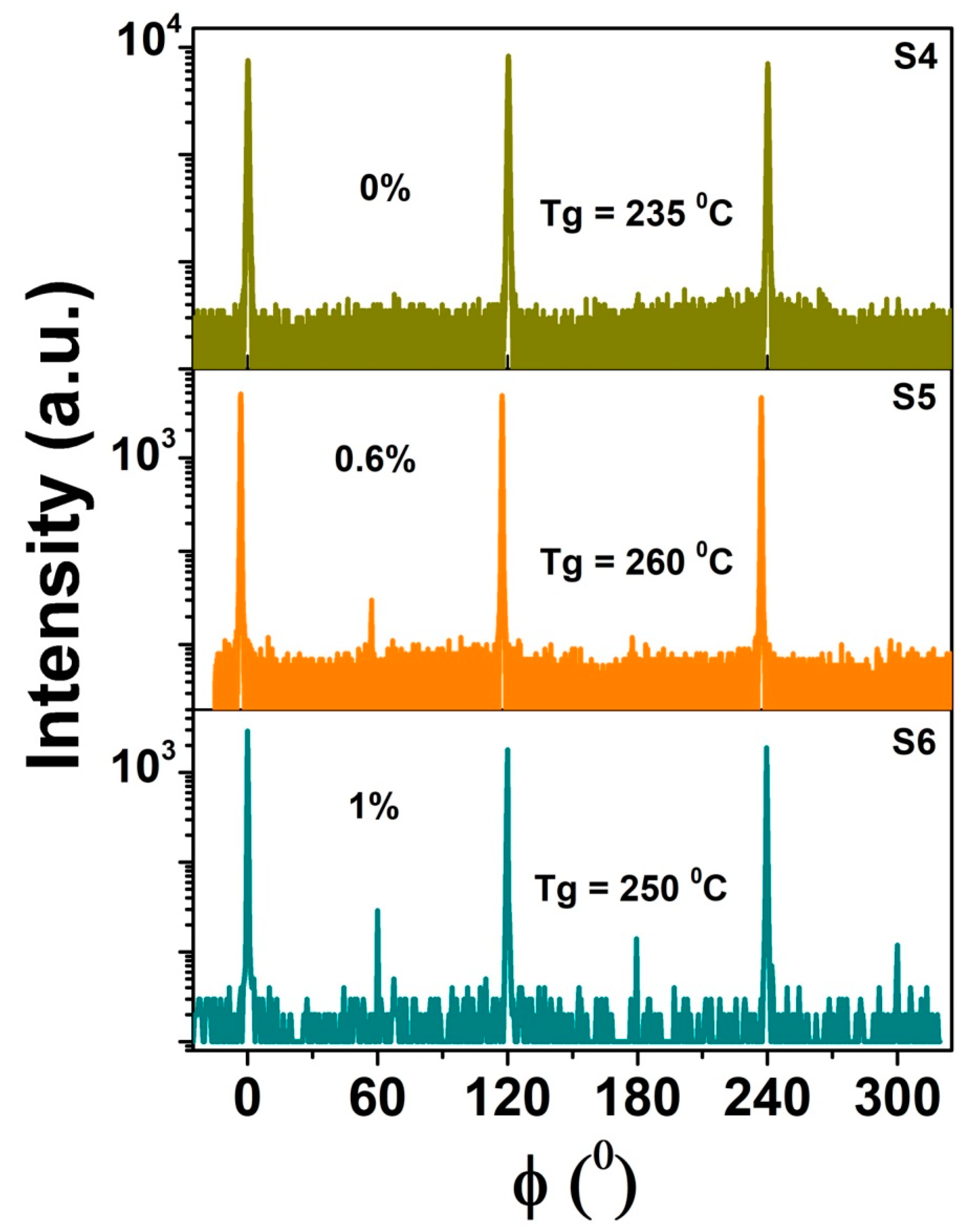
3.2. Structural Properties of the Grown Bi2Se3, and Sb2Te3 Epitaxial Layers

Bi2Se3 and Sb2Te3 layers were grown on the In2Se3/InP(111)B virtual substrate by MBE. The layers were grown at different growth temperatures (Tg = 245—295 °C) to establish the optimum value. An AFM image of an 18 nm thick Bi2Se3 film (sample S3) grown on the virtual substrate is shown in Figure 2d. The surface is composed of large terraces with a very small roughness of Rq = 0.5 nm. Figure 4a shows XRD 2θ-ω scans of a series of Bi2Se3 films with different thicknesses grown at different Tg. All the samples show peaks due to multiple reflections of (003) plane from Bi2Se3 layers with pronounced thickness fringes in both (003) and (006) reflections indicating high material and interface quality. As Bi2Se3 is closely lattice matched to In2Se3 (both α and β phases) the peaks due to reflections from the underlying In2Se3 layer cannot be distinguished. However, the peak broadening around the base of the (0015) and (0018) reflections gives evidence of the existence of this layer. Figure 4b shows XRD ϕ scans of the (015) plane of the three samples shown in Figure 4a. Full twin suppression was achieved for the sample S3 with the highest growth temperature (295 °C), whereas nearly full twin suppression (~0.5% twinning) was achieved for all the other samples grown throughout this temperature range. Again, the three peaks from the (015) plane do not always occur at the same in-plane angle as the (200) plane reflections of the substrate; rather, in some cases, the 60° rotation of the Bi2Se3 layer relative to the interface of the substrate is preferred [28], as observed for the In2Se3 layer. However, in either case, a single crystal layer with full twin suppression was achieved. For all the samples, the FWHM of the HRXRD rocking curve of the Bi2Se3 films is ~0.06° (see Supplemental Information Figure S1b), with an instrumental resolution of 0.004°. This is significantly lower than the FWHM reported in the literature [33], which is 0.30° with an instrumental resolution of 0.001° for the fully twin-suppressed Bi2Se3 grown on roughened InP(111)B substrates. The layer-twist of the samples is in the range of 0.2°–0.5° (determined by the FWHM of the peak of XRD ϕ scan, see Supplemental Information Figure S3b) and is comparable to the values found in the literature for the twin-suppressed samples grown on roughened InP(111)B substrate [33]. We conclude that the quality of the Bi2Se3 is improved significantly when grown on the smooth In2Se3 surfaces formed by our procedure rather than on rough InP surfaces.
In comparison to Bi2Se3, Sb2Te3 layers grown on these virtual substrates, exhibit a larger degree of roughness, as has been observed by others in the growth of Sb2Te3 [38]. Figure 2e,f show AFM images of Sb2Te3 (samples S4 and S6) with a roughness of 2.2 nm and 3.8 nm, respectively. When Sb2Te3 was grown on a Bi2Se3 layer, grown previously on the In2Se3 virtual substrate, the surfaces became even rougher than the ones directly grown on the In2Se3 (Figure 2f). Our results indicate that the use of the In2Se3 virtual substrate does not have an effect on the surface roughness of Sb3Te3. We conclude that, to reduce the surface roughness, a better understanding of the growth mechanism of Sb2Te3 would be needed. XRD 2θ-ω scans of Sb2Te3 on the In2Se3 layer and on the Bi2Se3/In2Se3 heterostructure are shown in Figure 5a. Since the In2Se3 is not lattice matched to Sb2Te3, 2θ-ω scans of S4 and S5 samples show two distinct sets of multiple reflections of the (003) plane; one set is due to the Sb2Te3 film, and the other set is due to the underlying In2Se3 layer, as marked in the Figure. XRD 2θ-ω scans of S6 show two distinct oscillations due to Bi2Se3 and Sb2Te3 layers, but the reflections due to In2Se3 overlap with the reflections of the Bi2Se3. Thickness fringes of the 2θ-ω scans due to these thin Sb2Te3 films are not observed possibly due to high interface roughness. Figure 5b shows XRR measurements of samples S4 and S5 which consist of oscillations with two distinct periods; oscillations with the short period are due to Sb2Te3 and the ones with the long period are due to In2Se3, from which we calculated the thickness of the two layers.
Figure 6 shows ϕ scans of (015) plane of these samples. Full twin suppression was achieved for Sb2Te3 grown on In2Se3 layers (sample S4), whereas Sb2Te3 grown on the Bi2Se3/In2Se3 heterostructure had a small degree (~1%) of twinning. The diminished quality of the Sb2Te3 grown on Bi2Se3 may be due to a non-optimal Tg that was used as a compromise for the structure, i.e., the growth temperature used is not the best for either layer. Optimization of the growth conditions may further reduce the twinning of these complex structures, which is desirable for the growth of Sb2Te3/Bi2Se3 superlattice structures with full twin suppression conditions. These superlattices have been shown to produce lower carrier-density materials due to superlattice gap enhancements [39].

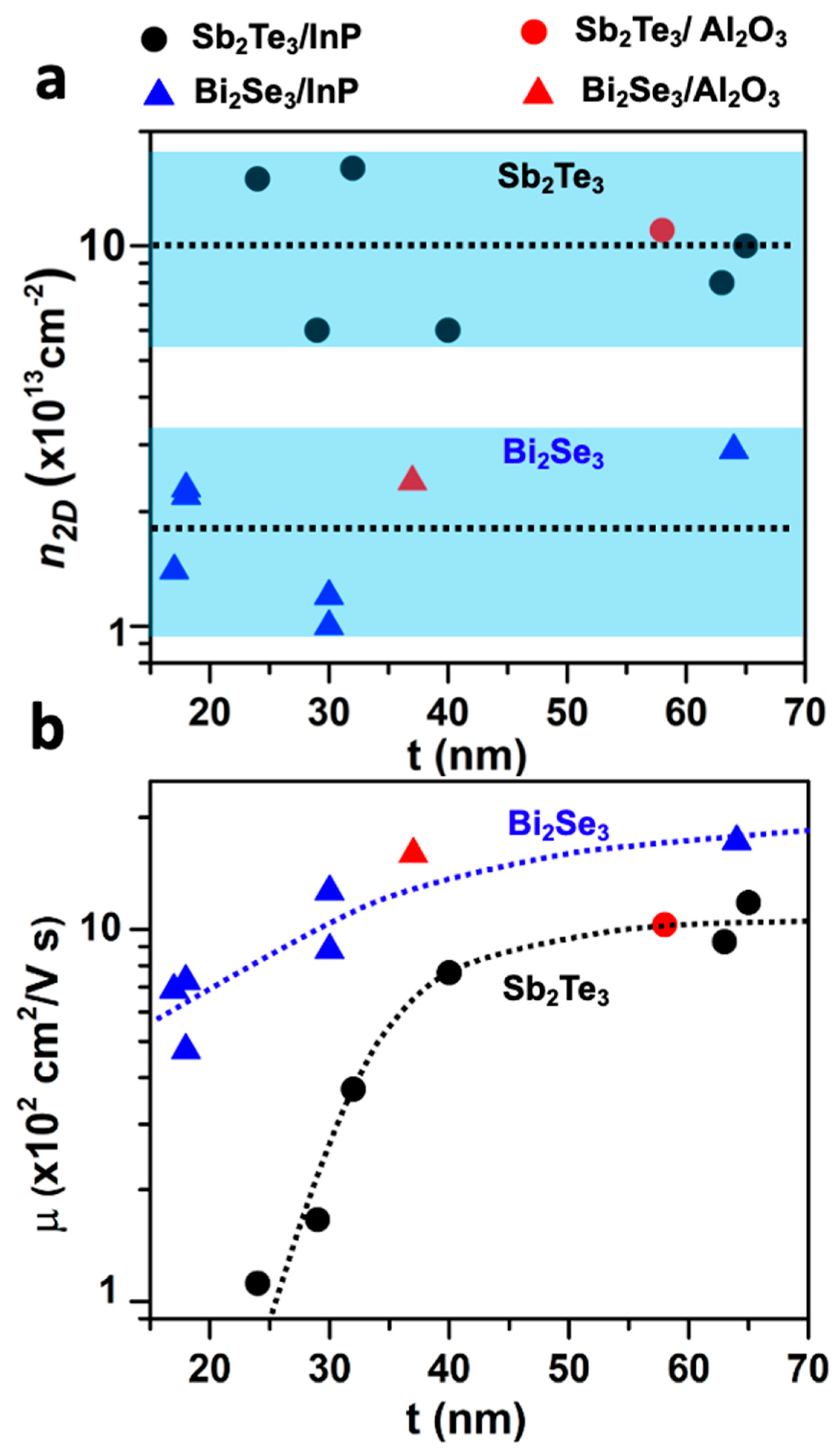
3.3. Transport Properties of Bi2Se3 and Sb2Te3

Surface preparation and substrate/epilayer interface are known to affect the transport properties of the TI layers. Figure 7a presents the thickness dependence of the 2D carrier density of Bi2Se3 and Sb2Te3 on In2Se3 virtual substrate. The data show that the variation in 2D carrier density is small, and there is no correlation between the layer thickness and the 2D carrier density of these materials. The average 2D carrier density of Bi2Se3 is ~2 × 1013 cm−2 (n-type) whereas for Sb2Te3 it is ~1 × 1014 cm−2(p-type), an order of magnitude higher. The average 2D carrier density of Bi2Se3 is ~2.5 times lower than the twinned Bi2Se3 grown directly on variety of substrates, which has previously been reported [40,41,42,43]. For comparison, we have shown the data for Bi2Se3 grown on Al2O3 in our MBE chamber, which had only 10% of twinning [44], as a red triangle on the plot. The previously reported lowest 2D carrier density for the fully twin-suppressed Bi2Se3 grown on roughened InP(111)B is 0.9 × 1013 cm−2, comparable to the lowest value we measured for twin-suppressed Bi2Se3, which is 1 × 1013 cm−2 (2D carrier density is calculated using the 3D carrier density of 100 nm thick Bi2Se3 given in the reference [33]). Therefore, we conclude that the electrical properties of Bi2Se3 samples grown on the In2Se3/InP(111)B virtual substrates are of comparable quality to the ones reported in the literature with low-twinning or fully twin-suppressed samples. On the other hand, the 2D carrier density of our un-twinned Sb2Te3 does not decrease compared to the twinned samples (red circle on the plot shows the 2D carrier density of Sb2Te3 grown on Al2O3 in the same MBE system), probably because the contribution from the other defects outweighs the ones from the suppressed twinning. Figure 7b shows the thickness dependence of the carrier mobility of the Bi2Se3 and Sb2Te3 layers. Carrier mobility of Sb2Te3 exhibits a steep decrease below ~40 nm whereas, for Bi2Se3, there is a slow and gradual decrease. This indicates that the Sb2Te3/In2Se3 interface has a larger density of scattering centers compared to the Bi2Se3/In2Se3 interface. This is likely due to the lattice mismatch at the Sb2Te3/In2Se3 interface, which may lead to more scattering centers. It may also be possible that there is intermixing or reacting of In and Se atoms with the Sb2Te3 layer at the interface. For thicker layers (layers thicker than 40 nm), carrier mobility of Sb2Te3 grown on Al2O3 falls along the same line as the twin-suppressed samples, as shown by the red circle in Figure 7b. Furthermore, the carrier mobility of the 10% twinned Bi2Se3 on Al2O3 follows the carrier mobility trend of the fully twin-suppressed Bi2Se3/In2Se3 layers presented here.
Bulk carriers in MBE-grown TIs are known to originate mainly from two sources, bulk defects and interface defects. As the names imply, bulk defects are generated in the bulk of the crystal and consist of anti-site defects and Se(Te)-vacancies [45], whereas the interface defects originate at the interface. Bulk defects may stay constant throughout the crystal or may progressively increase with the layer thickness. In the latter case, the 2D carrier density varies as t 1 / 2 , where t is the layer thickness. On the other hand, the interface defects do not change with the increasing thickness; instead, carrier mobility increases due to the reduction in scattering from the interface. In our samples, the observation that the 2D carrier density is independent of layer thickness whereas carrier mobility significantly increases as a function of layer thickness suggest that the dominant contribution of bulk carriers originates from the interface and the defect density in the bulk is constant. Similar observations were previously reported for these materials grown on Al2O3 [26]. Since most carriers originate at the interface, it is reasonable to expect that the use of a thicker In2Se3 buffer layer would result in lower carrier densities in the TI layers.

4. Conclusions

In this study, we developed a novel selenium passivation technique to convert the 3D non-vicinal InP(111)B substrate surface into an In2Se3 2D van der Waals virtual substrate without using an indium cell. Smooth ultra-thin (~6 nm) In2Se3 layers were grown reproducibly using this new technique. The layers have good crystalline quality and exhibit no twinning. We have also shown that full twin suppression of Bi2Se3 and Sb2Te3 layers was achieved by growth on smooth non-vicinal InP(111)B via the use of the In2Se3/InP(111)B virtual substrate. These Bi2Se3 and Sb2Te3 layers have greatly improved crystalline quality over the twin-suppressed ones grown on roughened InP(111)B substrates. Furthermore, the electrical properties of these layers are comparable with those reported for other twin-suppressed layers. We propose that the absence of twins is achieved by suppressing In-atom mobility on the surface, which allows all the In2Se3 nucleation sites to be aligned to the InP(111) substrate, thus eliminating the possibility of twinned domains. Twin-suppressed TI layers have potential advantages for novel device applications that rely on selective interactions between polarized light and the spin helicity properties of the topological surface states. For example, it has been shown that twin suppression increases the helicity-dependent photo response which is predicted as a potential application in chip-scale polarimeters [14]. Hence, high quality TIs with full twin suppression greatly broadens possible device applications in the terahertz regime.

Supplementary Materials

The following supporting information can be downloaded at: https://www.mdpi.com/article/10.3390/cryst13040677/s1. Figure S1. High resolution X-ray diffraction rocking curve (RC) of (006) plane of: (a) 6 nm thick In2Se3 layer on InP(111)B substrate (i.e., In2Se3 virtual substrate) with a full width at half maximum (FWHM) of 0.06° and (b) 18 nm thick Bi2Se3 layer (sample S3) grown on an In2Se3 virtual substrate with a FWHM of 0.06°. Bragg reflection angle (2θ) of (006) In2Se3 and (006) Bi2Se3 are 18.863° and 18.559°, respectively. Figure S2. (a) ϕ scan of (015) plane of the un-twinned In2Se3 Sample 1. (b) Expanded view of the peak at 120° shown in (a) with a FWHM of 0.01°. Figure S3. (a) ϕ scans of (015) plane of the fully twin suppressed Bi2Se3 samples S3 (18 nm thick) and S7 (64 nm thick). (b) Expanded view of the middle peak of the triplet shown in (a). The middle peak of S3 shown in (b) is shifted −60° to align with the middle peak of S7 for the convenience of comparison.

Author Contributions

K.S.W. conceived and executed the research and MBE growth. K.S.W. and C.F. conducted the HR-XRD, XRR, AFM, and Hall transport measurements. K.S.W. and M.C.T. wrote and reviewed the manuscript. All authors contributed to interpretation of the data and discussions. All authors have read and agreed to the published version of the manuscript.

Funding

This research was funded by NSF grant numbers HRD-1547830 and HRD-2112550 (NSF CREST Center IDEALS). Partial support was also provided by NSF grant number DMR-2011738 (PAQM).

Data Availability Statement

All data are available from the corresponding author upon reasonable request.

Acknowledgments

We would like to acknowledge Thor Axtmann Garcia for helpful discussions, and the Nanofabrication Facility of CUNY Advanced Science Research Center (ASRC) for instrument use, scientific and technical assistance.

Conflicts of Interest

The authors declare no conflict of interest.

References

  1. Xia, Y.; Qian, D.; Hsieh, D.; Wray, L.; Pal, A.; Lin, H.; Bansil, A.; Grauer, D.; Hor, Y.S.; Cava, R.J.; et al. Observation of a large-gap topological-insulator class with a single Dirac cone on the surface. Nat. Phys. 2009, 5, 398–402. [Google Scholar] [CrossRef] [Green Version]
  2. Zhang, H.; Liu, C.-X.; Qi, X.-L.; Dai, X.; Fang, Z.; Zhang, S.-C. Topological insulators in Bi2Se3, Bi2Te3 and Sb2Te3 with a single Dirac cone on the surface. Nat. Phys. 2009, 5, 438–442. [Google Scholar] [CrossRef]
  3. Hasan, M.Z.; Kane, C.L. Colloquium: Topological insulators. Rev. Mod. Phys. 2010, 82, 3045–3067. [Google Scholar] [CrossRef] [Green Version]
  4. Qi, X.-L.; Zhang, S.-C. The quantum spin Hall effect and topological insulators. Phys. Today 2010, 63, 33–38. [Google Scholar] [CrossRef] [Green Version]
  5. Guo, M.; Wang, Z.; Xu, Y.; Huang, H.; Zang, Y.; Liu, C.; Duan, W.; Gan, Z.; Zhang, S.-C.; He, K.; et al. Tuning thermoelectricity in a Bi2Se3 topological insulator via varied film thickness. New. J. Phys. 2016, 18, 015008. [Google Scholar] [CrossRef]
  6. He, Q.L.; Hughes, T.L.; Armitage, N.P.; Tokura, Y.; Wang, K.L. Topological spintronics and magnetoelectronics. Nat. Mater. 2022, 21, 15–23. [Google Scholar] [CrossRef]
  7. Wu, F.; Zhang, R.-X.; Das Sarma, S. Three-dimensional topological twistronics. Phys. Rev. Res. 2020, 2, 022010. [Google Scholar] [CrossRef]
  8. Zhou, C.; Song, D.; Jiang, Y.; Zhang, J. Modification of the Hybridization Gap by Twisted Stacking of Quintuple Layers in a Three-Dimensional Topological Insulator Thin Film. Chin. Phys. Lett. 2021, 38, 057307. [Google Scholar] [CrossRef]
  9. Fu, L.; Kane, C.L. Superconducting Proximity Effect and Majorana Fermions at the Surface of a Topological Insulator. Phys. Rev. Lett. 2008, 100, 096407. [Google Scholar] [CrossRef] [Green Version]
  10. Tian, W.; Yu, W.; Shi, J.; Wang, Y. The Property, Preparation and Application of Topological Insulators: A Review. Materials 2017, 10, 814. [Google Scholar] [CrossRef] [Green Version]
  11. Chang, C.-Z.; Liu, C.-X.; MacDonald, A.H. Colloquium: Quantum anomalous Hall effect. Rev. Mod. Phys. 2023, 95, 011002. [Google Scholar] [CrossRef]
  12. Yao, J.D.; Shao, J.M.; Li, S.W.; Bao, D.H.; Yang, G.W. Polarization dependent photocurrent in the Bi2Te3 topological insulator film for multifunctional photodetection. Sci. Rep. 2015, 5, 14184. [Google Scholar] [CrossRef] [PubMed] [Green Version]
  13. Tu, C.-M.; Chen, Y.-C.; Huang, P.; Chuang, P.-Y.; Lin, M.-Y.; Cheng, C.-M.; Lin, J.-Y.; Juang, J.-Y.; Wu, K.-H.; Huang, J.-C.A.; et al. Helicity-dependent terahertz emission spectroscopy of topological insulator Sb2Te3 thin films. Phys. Rev. B 2017, 96, 195407. [Google Scholar] [CrossRef] [Green Version]
  14. Connelly, B.C.; de Coster, G.J.; Taylor, P.J. Helicity- and Azimuthal-Dependent Topological Photocurrents in Bi2Se3 using THz Spectroscopy. In Proceedings of the Conference on Lasers and Electro-Optics, San Jose, CA, USA, 15–20 May 2022. [Google Scholar]
  15. Hsieh, D.; Xia, Y.; Qian, D.; Wray, L.; Dil, J.H.; Meier, F.; Osterwalder, J.; Patthey, L.; Checkelsky, J.G.; Ong, N.P.; et al. A tunable topological insulator in the spin helical Dirac transport regime. Nature 2009, 460, 1101–1105. [Google Scholar] [CrossRef] [Green Version]
  16. Chen, J.; Qin, H.J.; Yang, F.; Liu, J.; Guan, T.; Qu, F.M.; Zhang, G.H.; Shi, J.R.; Xie, X.C.; Yang, C.L.; et al. Gate-Voltage Control of Chemical Potential and Weak Antilocalization in Bi2Se3. Phys. Rev. Lett. 2010, 105, 176602. [Google Scholar] [CrossRef] [Green Version]
  17. Richardella, A.; Zhang, D.M.; Lee, J.S.; Koser, A.; Rench, D.W.; Yeats, A.L.; Buckley, B.B.; Awschalom, D.D.; Samarth, N. Coherent heteroepitaxy of Bi2Se3 on GaAs (111)B. Appl. Phys. Lett. 2010, 97, 262104. [Google Scholar] [CrossRef]
  18. Ginley, T.P.; Wang, Y.; Law, S. Topological Insulator Film Growth by Molecular Beam Epitaxy: A Review. Crystals 2016, 6, 154. [Google Scholar] [CrossRef] [Green Version]
  19. Guo, X.; Xu, Z.J.; Liu, H.C.; Zhao, B.; Dai, X.Q.; He, H.T.; Wang, J.N.; Liu, H.J.; Ho, W.K.; Xie, M.H. Single domain Bi2Se3 films grown on InP(111)A by molecular-beam epitaxy. Appl. Phys. Lett. 2013, 102, 151604. [Google Scholar] [CrossRef] [Green Version]
  20. Koma, A. Van der Waals epitaxy for highly lattice-mismatched systems. J. Cryst. Growth 1999, 201–202, 236–241. [Google Scholar] [CrossRef]
  21. He, L.; Xiu, F.; Wang, Y.; Fedorov, A.V.; Huang, G.; Kou, X.; Lang, M.; Beyermann, W.P.; Zou, J.; Wang, K.L. Epitaxial growth of Bi2Se3 topological insulator thin films on Si (111). J. Appl. Phys. 2011, 109, 103702. [Google Scholar] [CrossRef] [Green Version]
  22. West, D.; Sun, Y.Y.; Wang, H.; Bang, J.; Zhang, S.B. Native defects in second-generation topological insulators: Effect of spin-orbit interaction on Bi2Se3. Phys. Rev. B 2012, 86, 121201. [Google Scholar] [CrossRef] [Green Version]
  23. Kampmeier, J.; Weyrich, C.; Lanius, M.; Schall, M.; Neumann, E.; Mussler, G.; Schäpers, T.; Grützmacher, D. Selective area growth of Bi2Te3 and Sb2Te3 topological insulator thin films. J. Cryst. Growth 2016, 443, 38–42. [Google Scholar] [CrossRef]
  24. Bansal, N.; Kim, Y.S.; Edrey, E.; Brahlek, M.; Horibe, Y.; Iida, K.; Tanimura, M.; Li, G.-H.; Feng, T.; Lee, H.-D.; et al. Epitaxial growth of topological insulator Bi2Se3 film on Si(111) with atomically sharp interface. Thin Solid. Films 2011, 520, 224–229. [Google Scholar] [CrossRef] [Green Version]
  25. Wang, Z.Y.; Li, H.D.; Guo, X.; Ho, W.K.; Xie, M.H. Growth characteristics of topological insulator Bi2Se3 films on different substrates. J. Cryst. Growth 2011, 334, 96–102. [Google Scholar] [CrossRef]
  26. Koirala, N.; Brahlek, M.; Salehi, M.; Wu, L.; Dai, J.; Waugh, J.; Nummy, T.; Han, M.-G.; Moon, J.; Zhu, Y.; et al. Record Surface State Mobility and Quantum Hall Effect in Topological Insulator Thin Films via Interface Engineering. Nano Lett. 2015, 15, 8245–8249. [Google Scholar] [CrossRef] [Green Version]
  27. Wang, Y.; Ginley, T.P.; Law, S. Growth of high-quality Bi2Se3 topological insulators using (Bi1-xInx)2Se3 buffer layers. J. Vac. Sci. Technol. B 2018, 36, 02D101. [Google Scholar] [CrossRef]
  28. Richardella, A.; Kandala, A.; Lee, J.S.; Samarth, N. Characterizing the structure of topological insulator thin films. APL Mater. 2015, 3, 083303. [Google Scholar] [CrossRef] [Green Version]
  29. Tarakina, N.V.; Schreyeck, S.; Borzenko, T.; Schumacher, C.; Karczewski, G.; Brunner, K.; Gould, C.; Buhmann, H.; Molenkamp, L.W. Comparative Study of the Microstructure of Bi2Se3 Thin Films Grown on Si(111) and InP(111) Substrates. Cryst. Growth Des. 2012, 12, 1913–1918. [Google Scholar] [CrossRef]
  30. Chen, Z.; Garcia, T.A.; De Jesus, J.; Zhao, L.; Deng, H.; Secor, J.; Begliarbekov, M.; Krusin-Elbaum, L.; Tamargo, M.C. Molecular Beam Epitaxial Growth and Properties of Bi2Se3 Topological Insulator Layers on Different Substrate Surfaces. J. Electron. Mater. 2014, 43, 909–913. [Google Scholar] [CrossRef] [Green Version]
  31. Schreyeck, S.; Tarakina, N.V.; Karczewski, G.; Schumacher, C.; Borzenko, T.; Brüne, C.; Buhmann, H.; Gould, C.; Brunner, K.; Molenkamp, L.W. Molecular beam epitaxy of high structural quality Bi2Se3 on lattice matched InP(111) substrates. Appl. Phys. Lett. 2013, 102, 041914. [Google Scholar] [CrossRef] [Green Version]
  32. Takagaki, Y.; Jenichen, B.; Tominaga, J. Giant corrugations in Bi2Se3 layers grown on high-index InP substrates. Phys. Rev. B 2013, 87, 245302. [Google Scholar] [CrossRef] [Green Version]
  33. Tarakina, N.V.; Schreyeck, S.; Luysberg, M.; Grauer, S.; Schumacher, C.; Karczewski, G.; Brunner, K.; Gould, C.; Buhmann, H.; Dunin-Borkowski, R.E.; et al. Suppressing Twin Formation in Bi2Se3 Thin Films. Adv. Mater. Interfaces 2014, 1, 1400134. [Google Scholar] [CrossRef] [Green Version]
  34. Liu, L.; Dong, J.; Huang, J.; Nie, A.; Zhai, K.; Xiang, J.; Wang, B.; Wen, F.; Mu, C.; Zhao, Z.; et al. Atomically Resolving Polymorphs and Crystal Structures of In2Se3. Chem. Mater. 2019, 31, 10143–10149. [Google Scholar] [CrossRef]
  35. Claro, M.S.; Grzonka, J.; Nicoara, N.; Ferreira, P.J.; Sadewasser, S. Wafer-Scale Fabrication of 2D β-In2Se3 Photodetectors. Adv. Opt. Mater. 2021, 9, 2001034. [Google Scholar] [CrossRef]
  36. Tang, C.; Sato, Y.; Watanabe, K.; Tanabe, T.; Oyama, Y. Selective crystal growth of indium selenide compounds from saturated solutions grown in a selenium vapor. Results Mater. 2022, 13, 100253. [Google Scholar] [CrossRef]
  37. Küpers, M.; Konze, P.M.; Meledin, A.; Mayer, J.; Englert, U.; Wuttig, M.; Dronskowski, R. Controlled Crystal Growth of Indium Selenide, In2Se3, and the Crystal Structures of α-In2Se3. Inorg. Chem. 2018, 57, 11775–11781. [Google Scholar] [CrossRef] [Green Version]
  38. Zeng, Z.; Morgan, T.A.; Fan, D.; Li, C.; Hirono, Y.; Hu, X.; Zhao, Y.; Lee, J.S.; Wang, J.; Wang, Z.M.; et al. Molecular beam epitaxial growth of Bi2Te3 and Sb2Te3 topological insulators on GaAs (111) substrates: A potential route to fabricate topological insulator p-n junction. AIP Adv. 2013, 3, 072112. [Google Scholar] [CrossRef]
  39. Levy, I.; Youmans, C.; Garcia, T.A.; Deng, H.; Alsheimer, S.; Testelin, C.; Krusin-Elbaum, L.; Ghaemi, P.; Tamargo, M.C. Designer Topological Insulator with Enhanced Gap and Suppressed Bulk Conduction in Bi2Se3/Sb2Te3 Ultrashort-Period Superlattices. Nano Lett. 2020, 20, 3420–3426. [Google Scholar] [CrossRef] [Green Version]
  40. Li, H.D.; Wang, Z.Y.; Kan, X.; Guo, X.; He, H.T.; Wang, Z.; Wang, J.N.; Wong, T.L.; Wang, N.; Xie, M.H. The van der Waals epitaxy of Bi2Se3 on the vicinal Si(111) surface: An approach for preparing high-quality thin films of a topological insulator. New. J. Phys. 2010, 12, 103038. [Google Scholar] [CrossRef]
  41. Wang, X.; He, X.; Guan, T.; Liao, J.; Lin, C.; Wu, K.; Li, Y.; Zeng, C. Transport properties of topological insulator Bi2Se3 thin films in tilted magnetic fields. Phys. E Low-Dimens. Syst. Nanostruct. 2012, 46, 236–240. [Google Scholar] [CrossRef]
  42. Glinka, Y.D.; Babakiray, S.; Lederman, D. Plasmon-enhanced electron-phonon coupling in Dirac surface states of the thin-film topological insulator Bi2Se3. J. Appl. Phys. 2015, 118, 135713. [Google Scholar] [CrossRef] [Green Version]
  43. Kim, N.; Lee, P.; Kim, Y.; Kim, J.S.; Kim, Y.; Noh, D.Y.; Yu, S.U.; Chung, J.; Kim, K.S. Persistent Topological Surface State at the Interface of Bi2Se3 Film Grown on Patterned Graphene. ACS Nano 2014, 8, 1154–1160. [Google Scholar] [CrossRef] [PubMed] [Green Version]
  44. Levy, I.; Garcia, T.A.; Shafique, S.; Tamargo, M.C. Reduced twinning and surface roughness of Bi2Se3 and Bi2Te3 layers grown by molecular beam epitaxy on sapphire substrates. J. Vac. Sci. Technol. B 2018, 36, 02D107. [Google Scholar] [CrossRef]
  45. Navrátil, J.; Horák, J.; Plecháček, T.; Kamba, S.; Lošt’ák, P.; Dyck, J.S.; Chen, W.; Uher, C. Conduction band splitting and transport properties of Bi2Se3. J. Solid. State Chem. 2004, 177, 1704–1712. [Google Scholar] [CrossRef]
Figure 1. Reflection high-energy electron diffraction (RHEED) images of the InP(111)B surface (a) at Tsub = 200 °C, (b) at Tsub = 495 °C before anneal, and (c) at Tsub = 505 °C after 5 min anneal, i.e., the deoxidized surface with the newly formed In2Se3 layer via Se passivation of InP(111)B substrate. RHEED patterns are obtained along [ 0 1 ¯ 1 ] direction of the substrate. (d) Atomic force microscopy (AFM) image of the sample shown in (c) with smooth atomically flat In2Se3 layer which has a rot mean square roughness of Rq = 0.4 nm.
Crystals 13 00677 g001
Figure 2. Reflection high-energy electron diffraction (RHEED) images (a) after Bi2Se3 growth, (b) after Sb2Te3 growth, and (c) after the growth of Sb2Te3/Bi2Se3 stack. RHEED patterns are obtained along [ 0 1 ¯ 1 ] direction of the substrate. (e) An 18 nm thick Bi2Se3 film (sample S3) with a roughness of Rq = 0.5 nm, (f) a 29 nm thick Sb2Te3 film with a roughness of Rq = 2.2 nm (sample S4), and (d) a Sb2Te3/Bi2Se3 stack with a roughness of Rq = 3.8 nm (sample S6). Rq is the root mean square roughness of the surface.
Crystals 13 00677 g002
Figure 3. X-ray diffraction (XRD) (a) 2θ-ω scan of 6 nm thick In2Se3 layer; the inset shows X-ray reflectivity (XRR) of the In2Se3 layer with distinguishable oscillations. (b) ϕ scan of (015) plane of two different samples of In2Se3 and the (002) plane of InP(111)B substrate.
Crystals 13 00677 g003
Figure 4. X-ray diffraction (XRD) (a) 2θ-ω scans of Bi2Se3 films with different thicknesses grown at different substrate temperatures (Tg) on In2Se3 layer. (b) ϕ scan of (015) plane of the samples shown in (a) with the calculated twinning percentages.
Crystals 13 00677 g004
Figure 5. X-ray diffraction (XRD) (a) 2θ-ω scans of Sb2Te3 films with different thicknesses grown at different substrate temperatures (Tg) on In2Se3 layer. (b) Sample X-ray reflectivity (XRR) scan of Sb2Te3 films showing two distinct oscillations corresponding to In2Se3 and the Sb2Te3, from which the layer thicknesses are calculated.
Crystals 13 00677 g005
Figure 6. ϕ scan of (015) plane of the Sb2Te3 and Sb2Te3/Bi2Se3 samples shown in Figure 5a with the calculated twinning percentages. The dominant set of triplets shown here occurs at the same in-plane angle as the (200) plane reflections of the substrate.
Crystals 13 00677 g006
Figure 7. (a) 2D carrier density and (b) carrier mobility of Bi2Se3 and Sb2Te3 on In2Se3/InP(111)B as a function of film thickness. The red circle and the triangle are representative values of films grown on Al2O3 for film thickness of 37 nm Bi2Se3 and 58 nm Sb2Te3, respectively. Measurements are taken at 10 K.
Crystals 13 00677 g007
Table 1. Samples presented in the study. All samples were grown on virtual In2Se3/InP(111)B substrates.
Sample NumberMaterialGrowth Temperature (°C)Layer Thickness (nm)
S1Bi2Se324518
S2Bi2Se327030
S3Bi2Se329518
S4Sb2Te323529
S5Sb2Te326032
S6Sb2Te3 on Bi2Se325039
Disclaimer/Publisher’s Note: The statements, opinions and data contained in all publications are solely those of the individual author(s) and contributor(s) and not of MDPI and/or the editor(s). MDPI and/or the editor(s) disclaim responsibility for any injury to people or property resulting from any ideas, methods, instructions or products referred to in the content.

