
Long-Term Stability of Novel Crucible Systems for the Growth of Oxygen-Free Czochralski Silicon Crystals
 ,
, 
Abstract
:1. Introduction
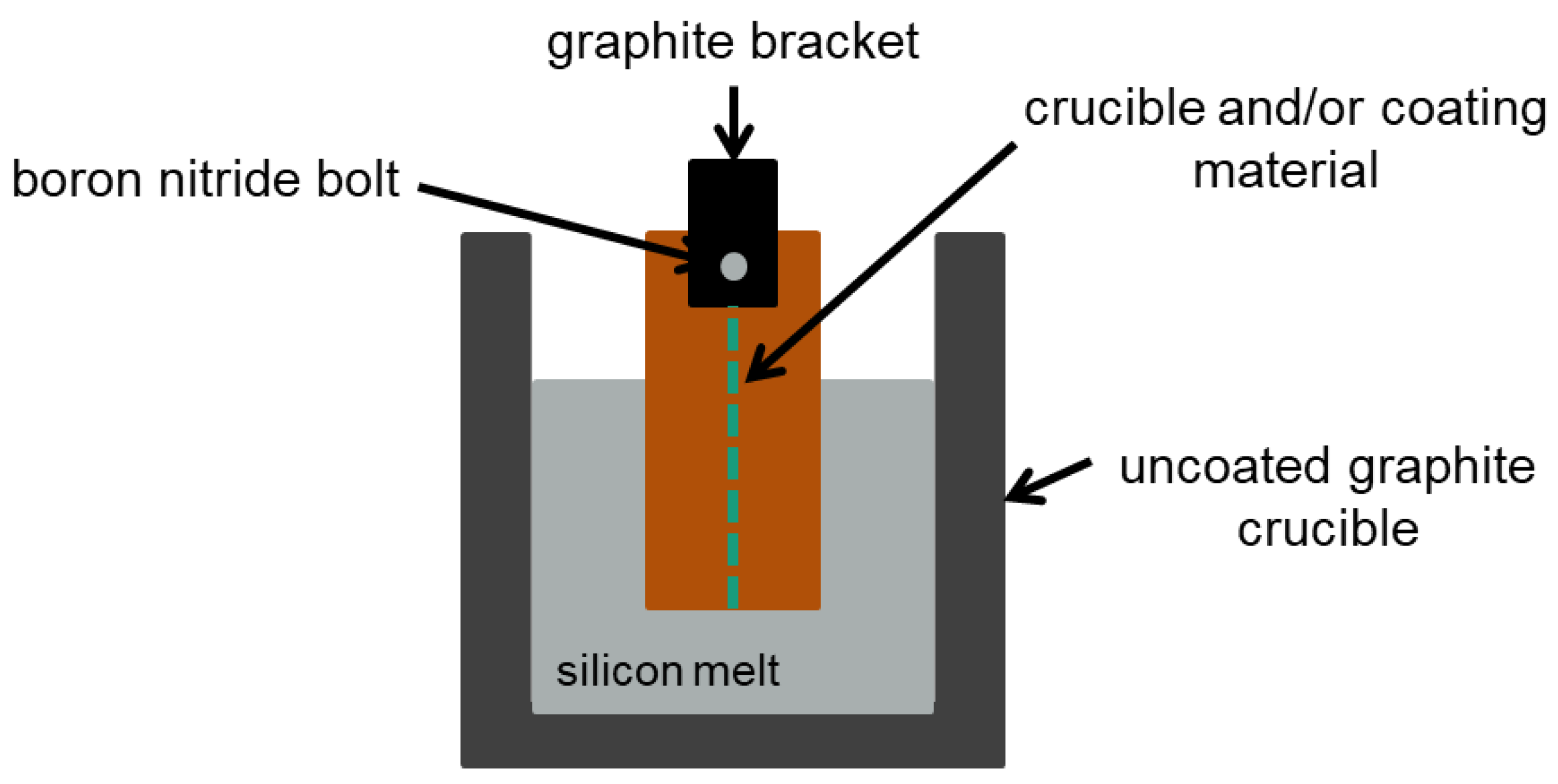
2. Materials and Methods
3. Results and Discussion
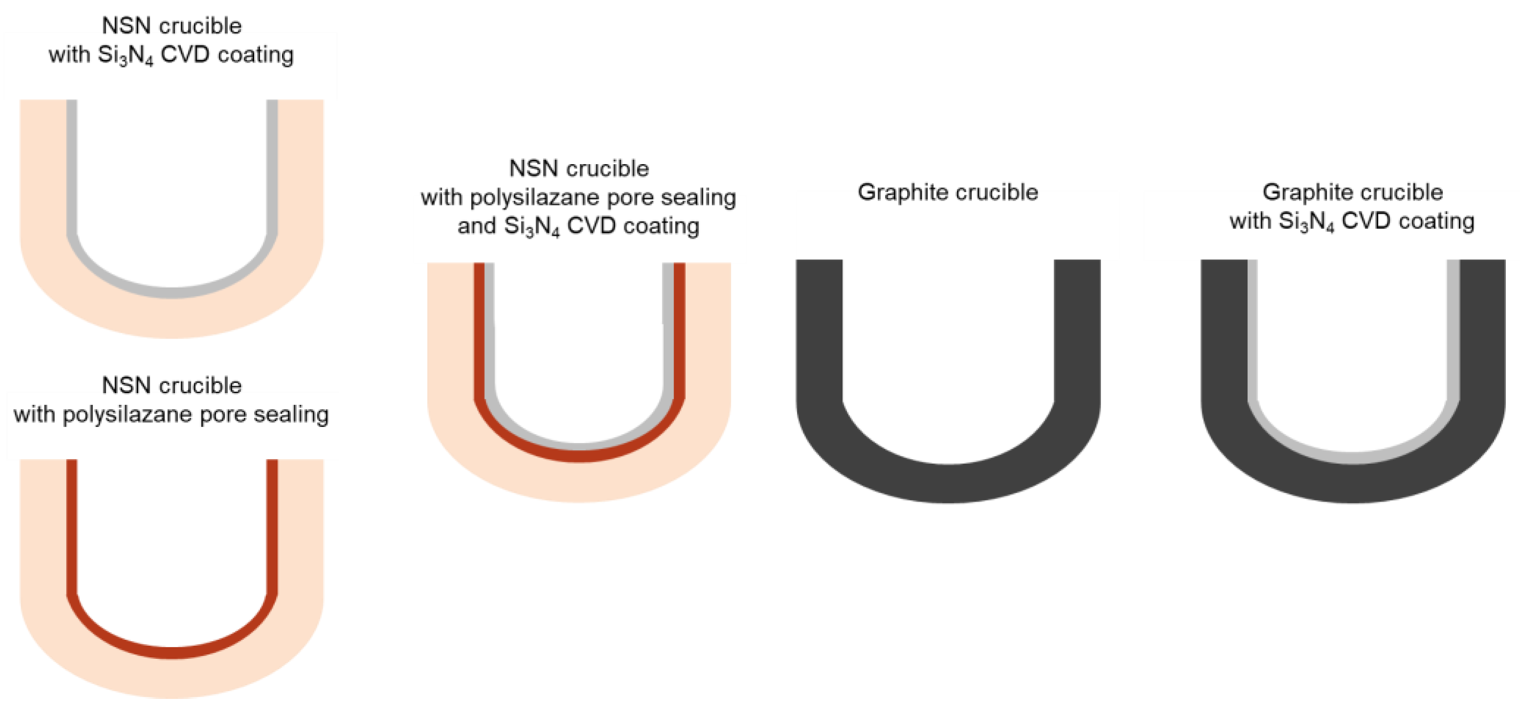
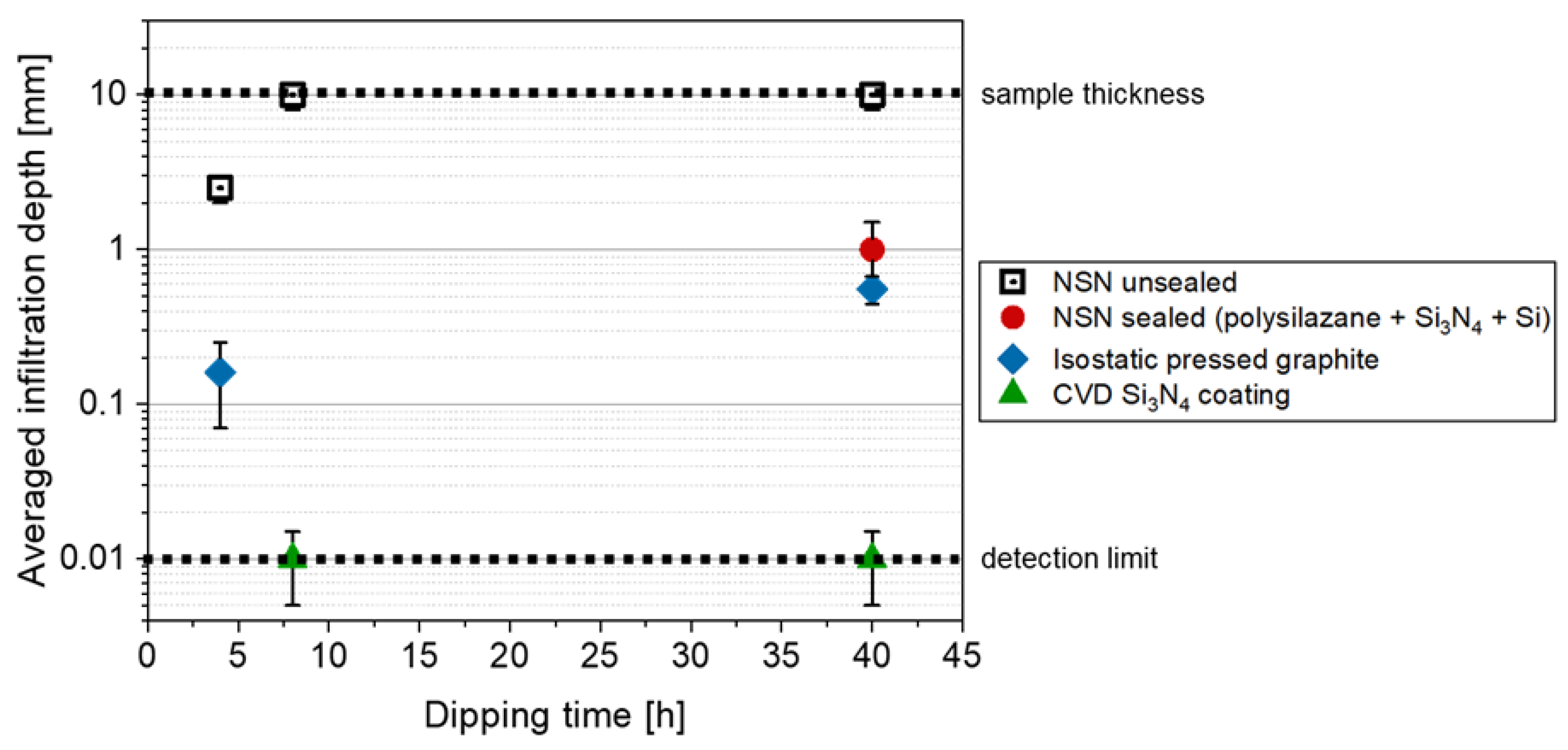
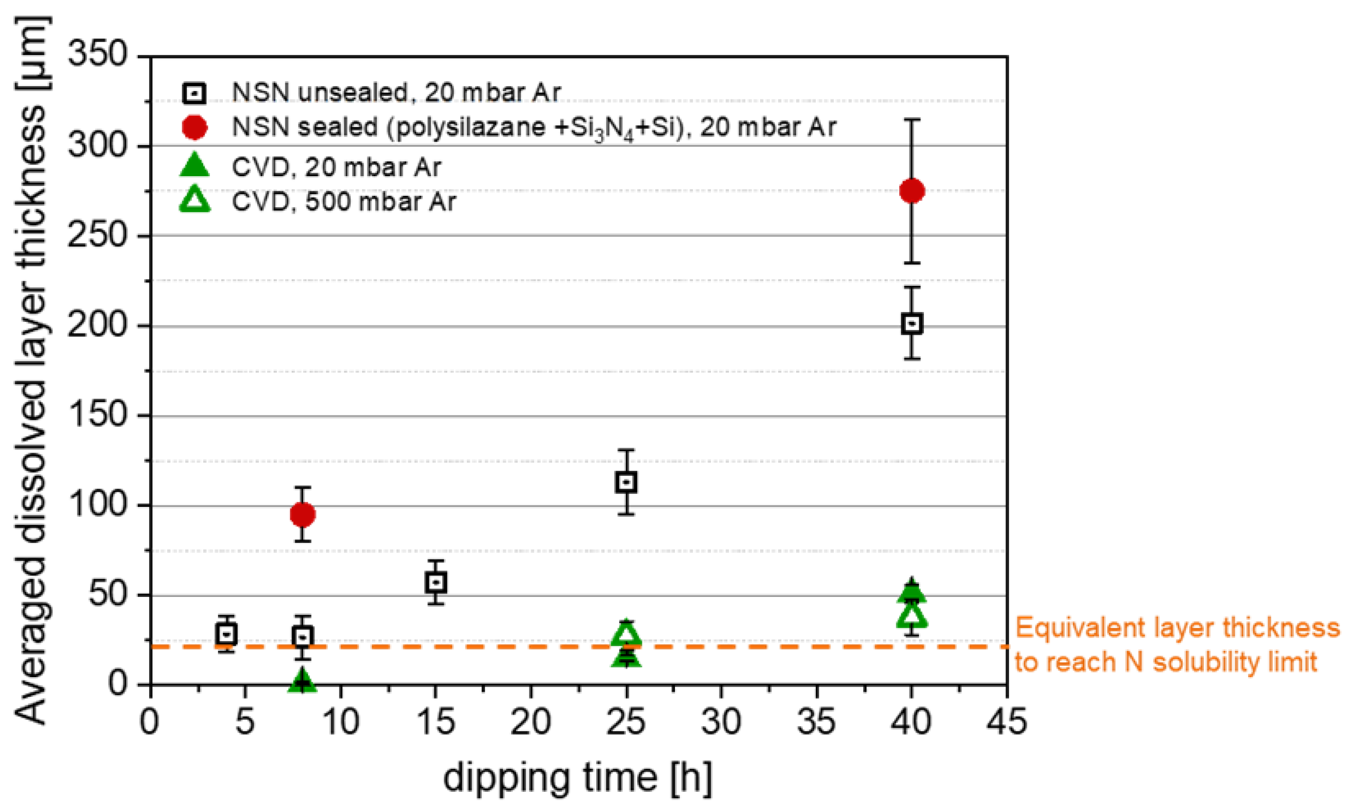
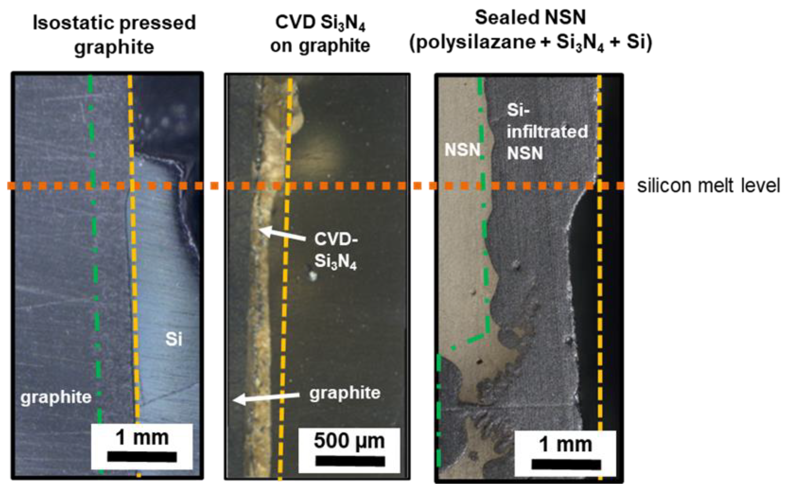
3.1. Dipping Experiments
3.2. Long Term Crystallization Experiments in G0 Scale
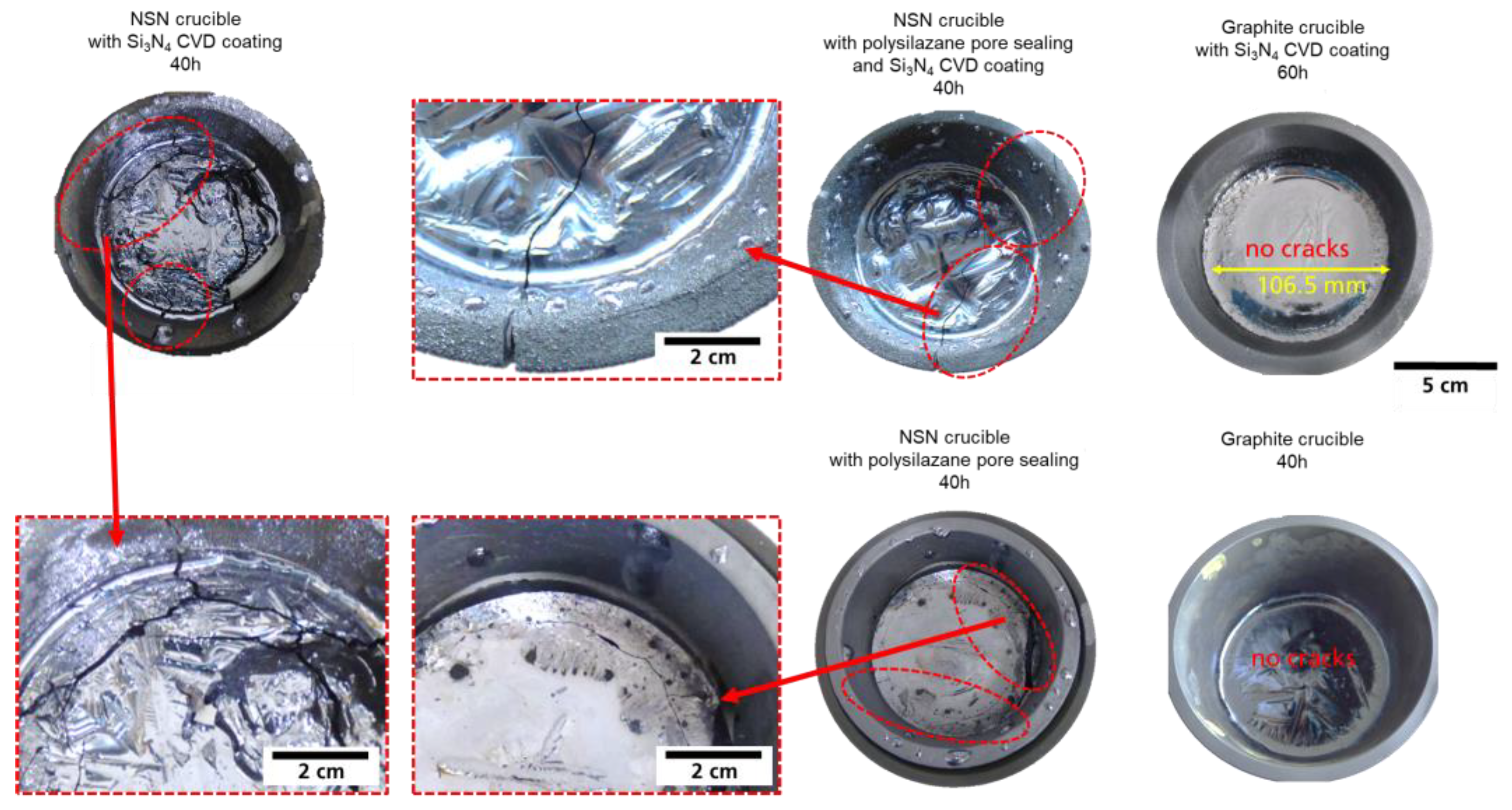
3.2.1. Performance and Durability of the Oxygen-Free Crucible Systems
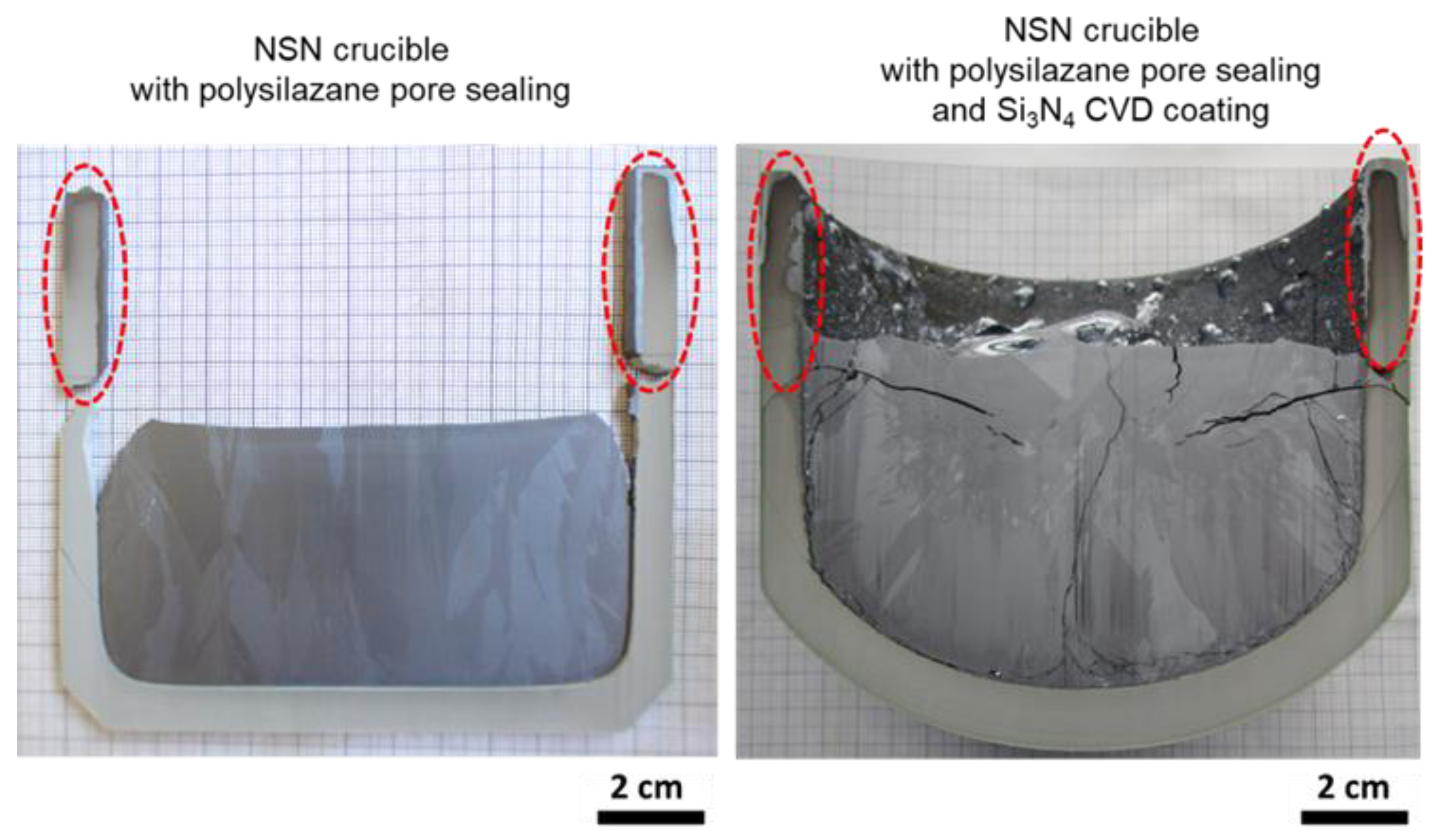
NSN Crucibles
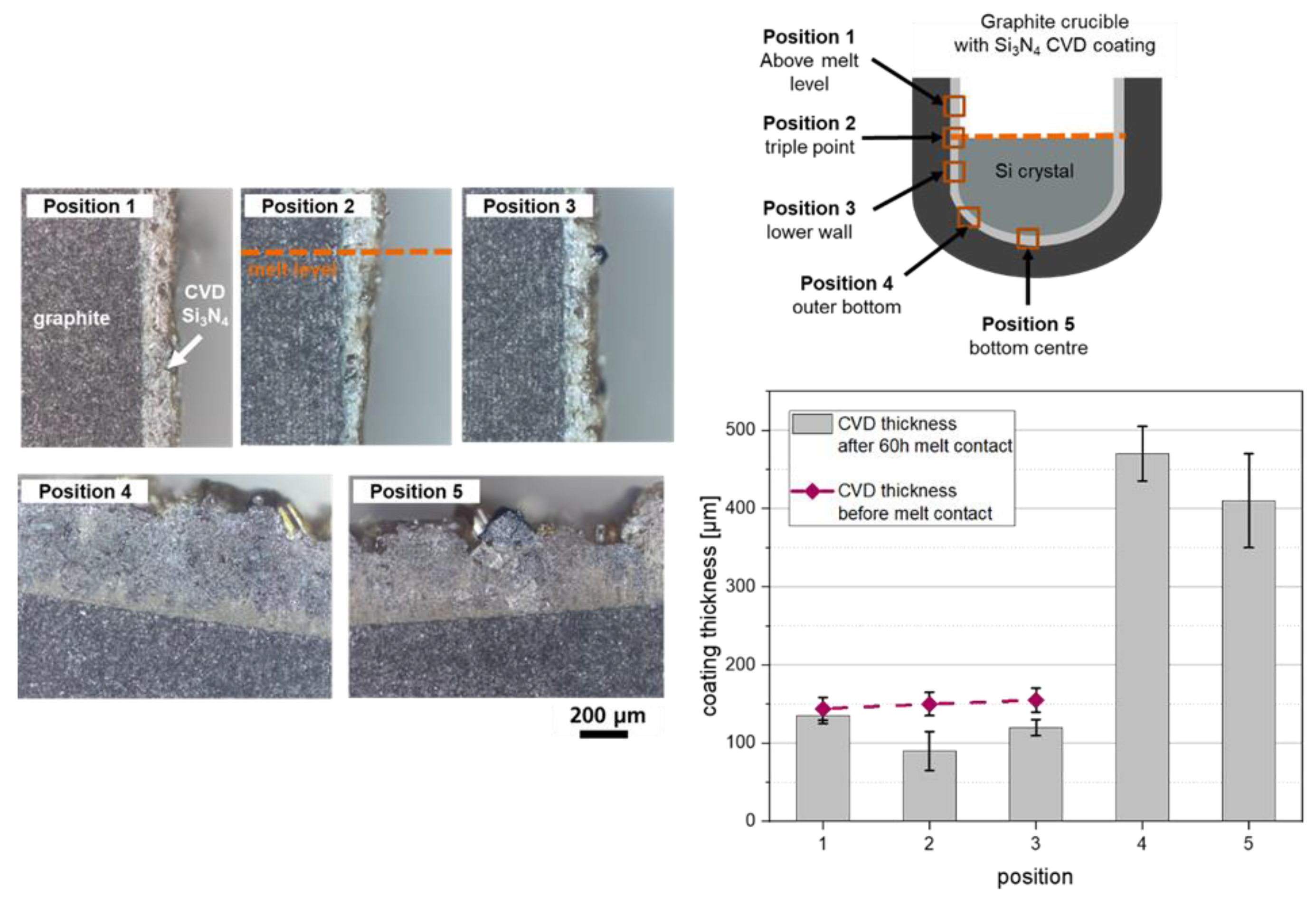
Graphite Crucibles
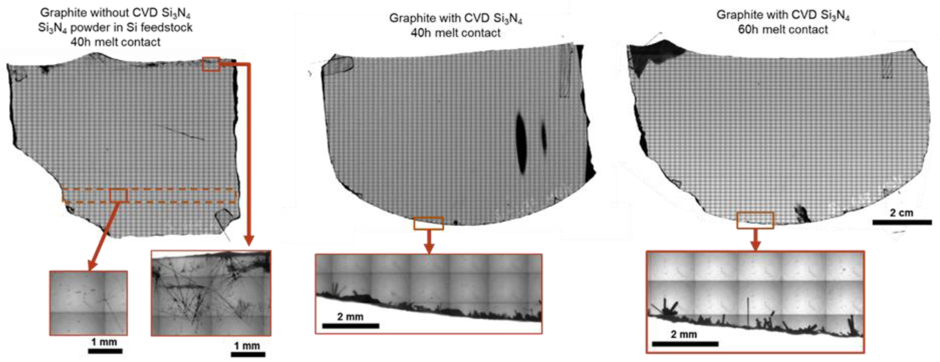
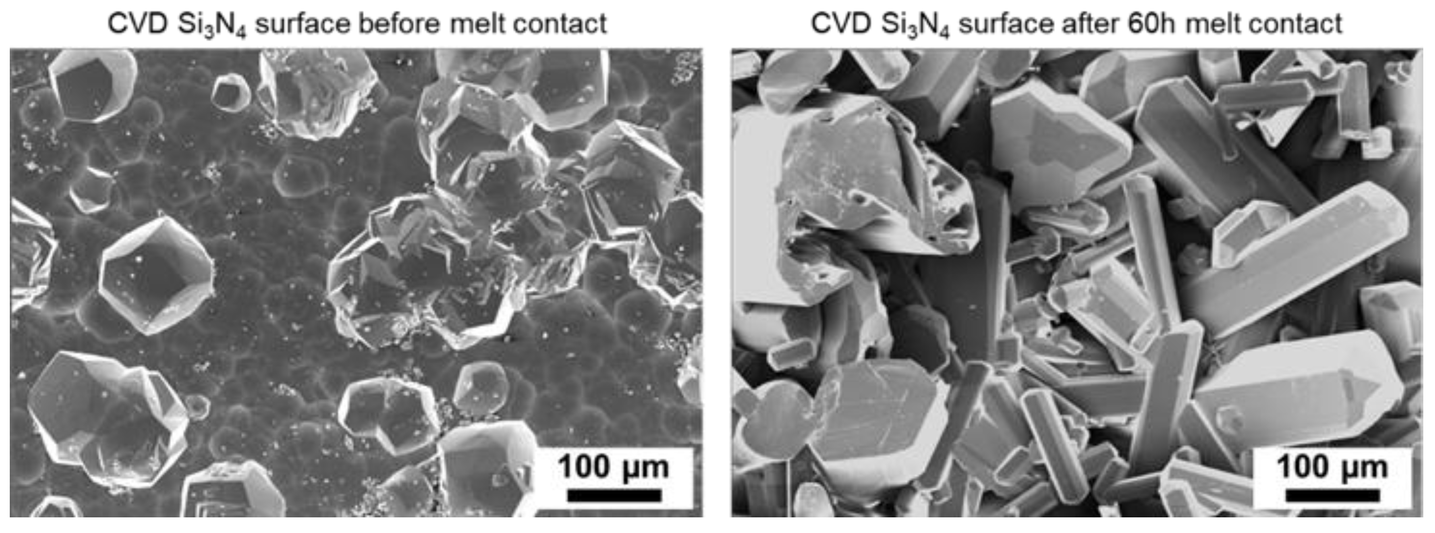
CVD Coating
3.2.2. Impact of Crucible/Coating Systems on Precipitate Formation in Grown Crystals
4. Conclusions
Author Contributions
Funding
Data Availability Statement
Acknowledgments
Conflicts of Interest
References
- Schulze, H.J.; Öfner, H.; Niedernostheide, F.J.; Laven, J.G.; Felsl, H.P.; Voss, S.; Schwagmann, A.; Jelinek, M.; Ganagona, N.; Susiti, A.; et al. Use of 300 mm magnetic Czochralski wafers for the fabrication of IGBTs. In Proceedings of the 28th International Symposium on Power Semiconductor Devices and ICs (ISPSD), Prague, Czech Republic, 12–16 June 2016; pp. 355–358. [Google Scholar]
- Kajiwara, K.; Harada, K.; Torigoe, K.; Hourai, M. Oxygen Precipitation Properties of Nitrogen-Doped Czochralski Silicon Single Crystals with Low Oxygen Concentration. Phys. Status Solidi (A) 2019, 216, 1900272. [Google Scholar] [CrossRef]
- Hourai, M.; Nagashima, T.; Nishikawa, H.; Sugimura, W.; Ono, T.; Umeno, S. Review and Comments for the Development of Point Defect-Controlled CZ-Si Crystals and Their Application to Future Power Devices. Phys. Status Solidi (A) Appl. Mater. Sci. 2019, 216, 1800664. [Google Scholar] [CrossRef]
- Kiyoi, A.; Kawabata, N.; Nakamura, K.; Fujiwara, Y. Influence of oxygen on trap-limited diffusion of hydrogen in proton-irradiated n -type silicon for power devices. J. Appl. Phys. 2021, 129, 025701. [Google Scholar] [CrossRef]
- Schulze, H.-J.; Öfner, H.; Niedernostheide, F.-J.; Lükermann, F.; Schulz, A. Fabrication of Medium Power Insulated Gate Bipolar Transistors Using 300 mm Magnetic Czochralski Silicon Wafers. Phys. Status Solidi (A) 2019, 216, 1900235. [Google Scholar] [CrossRef]
- Doi, H.; Kikuchi, N.; Oosawa, Y. Chemical vapour deposition coating of crystalline Si3N4 on a quartz crucible for nitrogen-doped Czochralski silicon crystal growth. Mater. Sci. Eng. A 1988, 105/106, 465–480. [Google Scholar] [CrossRef]
- Watanabe, M.; Usami, T.; Muraoka, H.; Matsuo, S.; Imanishi, Y.; Nagashima, H. Oxygen-Free Silicon Single Crystal Grown from Silicon Nitride Crucible. In Semiconductor Silicon 1981: Proceedings of the 4th International Symposium on Silicon Materials Science and Technology; Huff, H.R., Ed.; The Electrochemical Society: Pennington, NJ, USA, 1981; pp. 126–137. [Google Scholar]
- Matsuo, S.; Imanishi, Y.; Nagashima, H.; Watanabe, M.; Usami, T.; Muraoka, H. Device made of silicon nitride for pulling single crystal made of silicon and method of manufacturing the same. patent EP 0065122, 24 April 1982. [Google Scholar]
- Nakajima, K.; Morishita, K.; Murai, R.; Usami, N. Formation process of Si3N4 particles on surface of Si ingots grown using silica crucibles with Si3N4 coating by noncontact crucible method. J. Crys. Growth 2014, 389, 112–119. [Google Scholar] [CrossRef] [Green Version]
- Huguet, C.; Dechamp, C.; Camel, D.; Drevet, B.; Eustathopoulos, N. Study of interactions between silicon and coated graphite for application to photovoltaic silicon processing. J. Mater. Sci. 2019, 54, 11546–11555. [Google Scholar] [CrossRef]
- Camel, D.; Cierniak, E.; Drevet, B.; Cabal, R.; Ponthenier, D.; Eustathopoulos, N. Directional solidification of photovoltaic silicon in re-useable graphite crucibles. Sol. Energy Mater. Sol. Cells 2020, 215, 110637. [Google Scholar] [CrossRef]
- Hendawi, R.; Arnberg, L.; Di Sabatino, M. Novel coatings for graphite materials in PV silicon applications: A study of the surface wettability and interface interactions. Sol. Energy Mater. Sol. Cells 2022, 234, 111422. [Google Scholar] [CrossRef]
- Schneider, V.; Reimann, C.; Friedrich, J.; Müller, G. Nitride bonded silicon nitride as a reusable crucible material for directional solidification of silicon. Cryst. Res. Technol. 2016, 51, 74–86. [Google Scholar] [CrossRef]
- Bellmann, M.P.; Noja, G.; Ciftja, A. Eco-Solar Factory: Utilisation of Kerf-Loss from Silicon Wafer Sawing for the Manufacturing of Silicon Nitride Crucibles. In Proceedings of the 35th European Photovoltaic Solar Energy Conference, Brussels, Belgium, 24–28 September 2018; pp. 501–502. [Google Scholar]
- Hendawi, R.; Ciftja, A.; Stokkan, G.; Arnberg, L.; Di Sabatino, M. The effect of preliminary heat treatment on the durability of reaction bonded silicon nitride crucibles for solar cells applications. J. Crys. Growth 2020, 542, 125670. [Google Scholar] [CrossRef]
- Lan, A.; Liu, C.E.; Yang, H.L.; Yu, H.T.; Liu, I.T.; Hsu, H.P.; Lan, C.W. Silicon ingot casting using reusable silicon nitride crucibles made from diamond wire sawing kerf-loss silicon. J. Crys. Growth 2019, 525, 125184. [Google Scholar] [CrossRef]
- Knerer, D. Verfahren und Vorrichtung zum Ziehen eines Einkristalls und Halbleiterscheibe aus Silizium. DE 102018210286 A1, 25 June 2018. [Google Scholar]
- Hendawi, R.; Søndenå, R.; Ciftja, A.; Stokkan, G.; Arnberg, L.; Di Sabatino, M. Microstructure and electrical properties of multi- crystalline silicon ingots made in silicon nitride crucibles. AIP Conf. Proc. 2022, 2487, 130005. [Google Scholar] [CrossRef]
- Sturm, F.; Trempa, M.; Schuster, G.; Götz, P.; Wagner, R.; Barroso, G.; Meisner, P.; Reimann, C.; Friedrich, J. Material evaluation for engineering a novel crucible setup for the growth of oxygen free Czochralski silicon crystals. J. Cryst. Growth 2022, 584, 126582. [Google Scholar] [CrossRef]
- Mirkhalaf, M.; Yazdani Sarvestani, H.; Yang, Q.; Jakubinek, M.B.; Ashrafi, B. A comparative study of nano-fillers to improve toughness and modulus of polymer-derived ceramics. Sci. Rep. 2021, 11, 6951. [Google Scholar] [CrossRef] [PubMed]
- Barroso, G.; Li, Q.; Bordia, R.K.; Motz, G. Polymeric and ceramic silicon-based coatings—A review. J. Mater. Chem. A 2019, 7, 1936–1963. [Google Scholar] [CrossRef]
- Israel, R.; Voytovych, R.; Protsenko, P.; Drevet, B.; Camel, D.; Eustathopoulos, N. Capillary interactions between molten silicon and porous graphite. J. Mater. Sci. 2010, 45, 2210–2217. [Google Scholar] [CrossRef]
- Chaney, R.E.; Varker, C.J. The Erosion of Materials in Molten Silicon. J. Electrochem. Soc. 1976, 123, 846–852. [Google Scholar] [CrossRef]
- Eustathopoulos, N.; Israel, R.; Drevet, B.; Camel, D. Reactive infiltration by Si: Infiltration versus wetting: Viewpoint set no. 46 “Triple Lines”. Scr. Mater. 2010, 62, 966–971. [Google Scholar] [CrossRef]
- Hoseinpur, A.; Safarian, J. Mechanisms of graphite crucible degradation in contact with Si–Al melts at high temperatures and vacuum conditions. Vacuum 2020, 171, 108993. [Google Scholar] [CrossRef]
- Lian, P.; Huang, A.; Gu, H.; Zou, Y.; Fu, L.; Wang, Y. Towards prediction of local corrosion on alumina refractories driven by Marangoni convection. Ceram. Int. 2018, 44, 1675–1680. [Google Scholar] [CrossRef]
- Chaney, R.E.; Varker, C.J. The dissolution of fused silica in molten silicon. J. Cryst. Growth 1976, 33, 188–190. [Google Scholar] [CrossRef]
- Mukai, K. Wetting and Marangoni Effect in Iron and Steelmaking Processes. ISIJ Int. 1992, 32, 19–25. [Google Scholar] [CrossRef]
- Trempa, M.; Reimann, C.; Friedrich, J.; Müller, G. The influence of growth rate on the formation and avoidance of C and N related precipitates during directional solidification of multi crystalline silicon. J. Crys. Growth 2010, 312, 1517–1524. [Google Scholar] [CrossRef]


Disclaimer/Publisher’s Note: The statements, opinions and data contained in all publications are solely those of the individual author(s) and contributor(s) and not of MDPI and/or the editor(s). MDPI and/or the editor(s) disclaim responsibility for any injury to people or property resulting from any ideas, methods, instructions or products referred to in the content. |
© 2022 by the authors. Licensee MDPI, Basel, Switzerland. This article is an open access article distributed under the terms and conditions of the Creative Commons Attribution (CC BY) license (https://creativecommons.org/licenses/by/4.0/).
Share and Cite
Sturm, F.; Trempa, M.; Schuster, G.; Hegermann, R.; Goetz, P.; Wagner, R.; Barroso, G.; Meisner, P.; Reimann, C.; Friedrich, J. Long-Term Stability of Novel Crucible Systems for the Growth of Oxygen-Free Czochralski Silicon Crystals. Crystals 2023, 13, 14. https://doi.org/10.3390/cryst13010014
Sturm F, Trempa M, Schuster G, Hegermann R, Goetz P, Wagner R, Barroso G, Meisner P, Reimann C, Friedrich J. Long-Term Stability of Novel Crucible Systems for the Growth of Oxygen-Free Czochralski Silicon Crystals. Crystals. 2023; 13(1):14. https://doi.org/10.3390/cryst13010014
Chicago/Turabian StyleSturm, Felix, Matthias Trempa, Gordian Schuster, Rainer Hegermann, Philipp Goetz, Rolf Wagner, Gilvan Barroso, Patrick Meisner, Christian Reimann, and Jochen Friedrich. 2023. "Long-Term Stability of Novel Crucible Systems for the Growth of Oxygen-Free Czochralski Silicon Crystals" Crystals 13, no. 1: 14. https://doi.org/10.3390/cryst13010014