Article

Effect of Annealing Time on Structure, Morphology, and Optical Properties of Nanostructured CdO Thin Films Prepared by CBD Technique

by
Khalid Ridha Kadhim
and
Raghad Y. Mohammed
*
Department of Physics, College of Science, University of Duhok, Duhok 42001, Kurdistan Region, Iraq
*
Author to whom correspondence should be addressed.
Crystals 2022, 12(9), 1315; https://doi.org/10.3390/cryst12091315
Submission received: 27 August 2022 / Revised: 9 September 2022 / Accepted: 12 September 2022 / Published: 18 September 2022

Abstract

:
Nanostructured cadmium oxide (CdO) thin films were deposited onto glass substrates using the chemical bath deposition (CBD) technique. Different deposition parameters such as deposition time, bath temperature, pH, and CdSO4 concentration have been considered to specify the optimum conditions to obtain uniform and well-adherent thin films. The thin films prepared under these optimum conditions were annealed for different times (20, 40, and 60 min) at 300 °C, where no previous studies had been done to study the effect of annealing time. The XRD analysis showed that the as-deposited film is Cd(OH)2 with a hexagonal phase. While all the annealed films are CdO with a cubic phase. The crystallite size increases with the annealing time. However, the strain, dislocation density, and the number of crystallites were found to be decreased with annealing time. SEM images of annealed films showed a spherical nanoparticle with an average of particle size 80–46 nm. EDX analysis revealed that the ratio of cadmium to oxygen increases with increasing the annealing time to 40 min. The optical characterization shows that the transmittance is in the range of 63–73% and the energy gap is in the range of 2.61–2.56 eV. It has been found that the transmittance increased and the energy gap decreased with the annealing time. The prepared CdO films can be used in photodegradation applications to remove pollutants from water.

1. Introduction

Recently, transparent conducting oxides (TCOs) have attracted great significance in multiple areas of research due to their distinct properties such as high optical transmittance in the visible and NIR regions of the electromagnetic spectrum, wide bandgap energy, and unique electrical properties [1,2,3,4,5]. Among them, the CdO is an n-type metal oxide semiconductor from the II-VI group with an FCC crystal structure [6,7,8,9,10] that has a direct band gap from 2.2–2.7 eV [11,12]. These distinctive properties have made CdO one of the important candidate materials for multiple applications such as solar cells [13,14] photodetectors [15,16,17], gas sensors [18,19], and photocatalysis [20,21]. Cadmium oxide is very toxic by inhalation, oral, and dermal materials, but we use it due to its unique properties, various applications, and different features [22,23,24]. CdO thin films have been prepared by using different deposition techniques such as thermal evaporation [25], electron beam evaporation [26], pulsed-laser deposition [27], DC magnetron sputtering [28], RF magnetron sputtering [29], successive ionic layer adsorption and reaction (SILAR) [30], spray pyrolysis [31], sol-gel [32], and chemical bath deposition (CBD) [33,34,35,36]. CBD, also known as chemical solution deposition, is a simple, low-cost, and widely used technique to deposit TCO thin films using a simple setup. The substrate is placed inside a beaker containing a supersaturated solution of aqueous precursors such as mineral salts, complexing agents, and a pH stabilizer. CBD has numerous benefits, such as the ability to operate at atmospheric pressure and low temperatures, it does not need sophisticated instruments such as vacuum systems, can be used to deposit a large number of materials, the ability to deposit wide areas, and the possibility of adjusting the properties of thin films by controlling the deposition conditions [16,37,38].
These days, people are becoming more and more aware of the essential significance of a secure and healthy environment. As a result, detecting and treating hazardous chemicals is crucial. For water treatment, many techniques have been tested [21,39,40,41]. The photocatalytic method stands out among them as the approach to purge pollutants from aqueous solutions that offers the most promise. In this arena, nanotechnology is important, and semiconductor nanoparticles have already been shown to be useful for treating water [42,43]. The two most popular metal oxide-based semiconductor materials are ZnO and TiO2 metal oxides [44,45,46,47,48,49]. Much lower data have been reported for the CdO system [50,51].
On the other hand, CBD has some drawbacks such as wastage of materials due to the homogeneous reaction in the reaction bath, and not being able to work at high temperatures (90 °C and above) unless the deposition time is short due to evaporation of the aqueous solution [38,52], and the required thin films have not been obtained directly, as in this work, where the annealing process is required to convert the deposited thin films from Cd(OH)2 to CdO thin films. Additionally, Cd(OH)2 is an important precursor that can be converted to other important compounds such as CdS and CdSe by reaction with appropriate additives [53,54]. Moreover, it is considered a commonly utilized semiconductor in optoelectronics and solar cell applications due to its wide bandgap energy (2.75–3.5 eV), high optical transmittance in the visible range of the electromagnetic spectrum, and high electrical conductivity compared to some else semiconductors [55,56,57].
Furthermore, to the best of the researchers’ knowledge, there is no previous report on the effect of annealing time on the properties of CdO thin films prepared by the CBD technique.
Therefore, the novelty and importance of this work include the preparation and investigation of the effect of annealing time on structural, morphological, and optical properties of CdO thin films obtained by the CBD technique. Moreover, this includes the optimization of major deposition parameters to obtain uniform and well-adherent thin films. Additionally, the ability of the prepared CdO films will be examined for photodegradation application to remove pollutants from water, and this work is currently in progress (MSc student’s work).

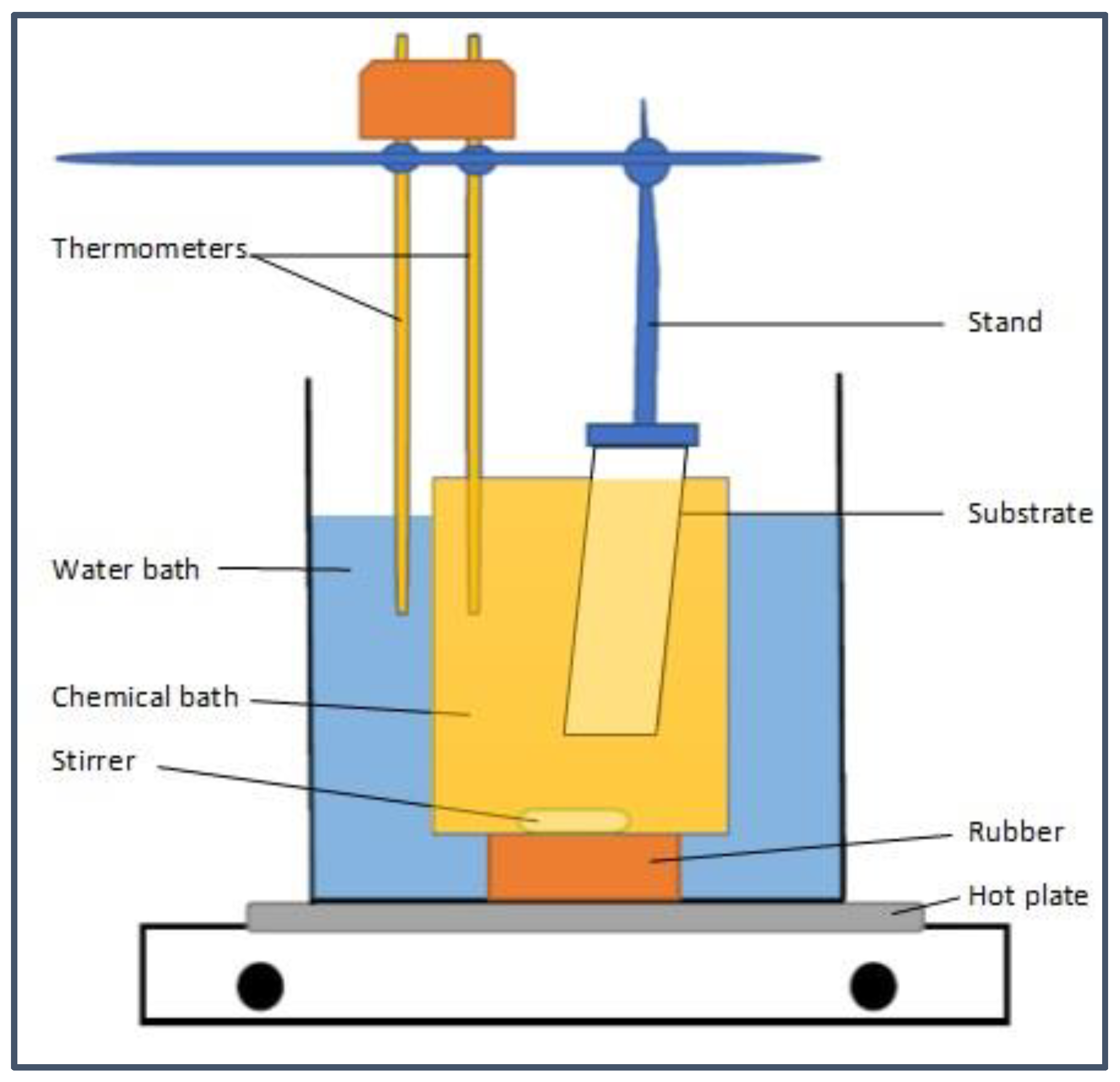
2. Experimental Details

2.1. Materials

CdO thin films were prepared by using the CBD technique. Cadmium sulfate (CdSO4) salt was used as a Cd2+ ions, ammonium hydroxide (NH4OH) as a complexing agent, and hydrogen peroxide (H2O2). Ammonium hydroxide acted as both a complexing agent and a pH stabilizer in the alkaline medium. Furthermore, it represented a source of OH ions, while H2O2 plays an important role in avoiding spontaneous precipitation of any solid phase in the reaction. In this work, all utilized chemical materials were bought from Sigma-Aldrich company without further purification. Distilled water has been used for synthesis and treatment processes.

2.2. Substrate Cleaning

The soda-lime glass slide with the dimension of (25 × 75 × 1) mm3 was used as the substrate for CdO thin film synthesis. Before the synthesis, the glass substrates have been cleaned by soaking them in chromic acid (H2CrO4) for 24 h, washed with distilled water, and ultrasonically cleaned with acetone (C3H5OH) for 15 min. Finally, dried in air at room temperature, and kept in a desiccator [58]. The mentioned cleaning process provides good adhesion, growth nucleation center, and uniform synthesis of thin films [59].

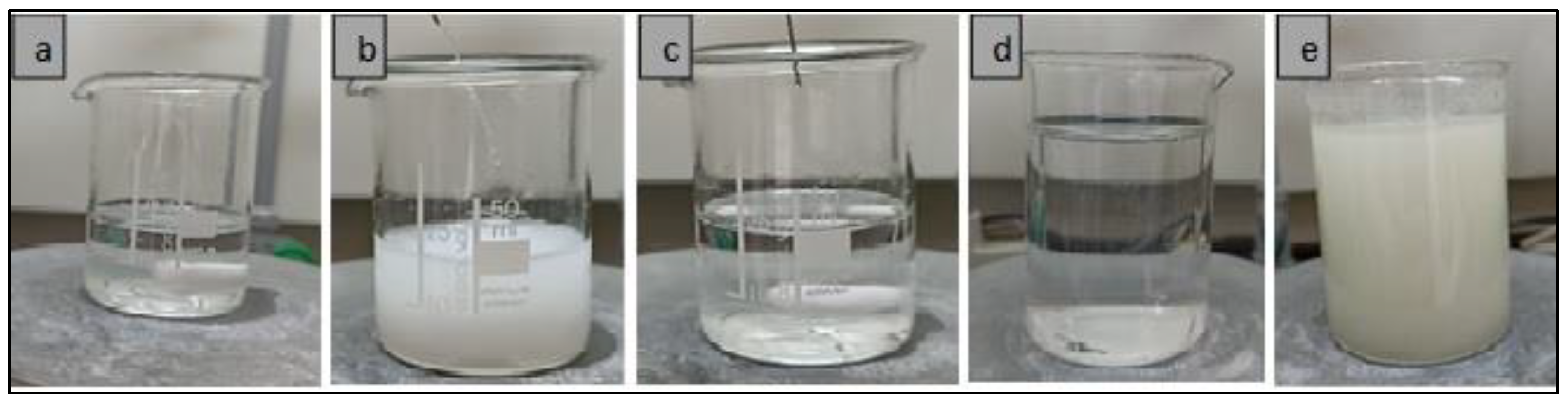
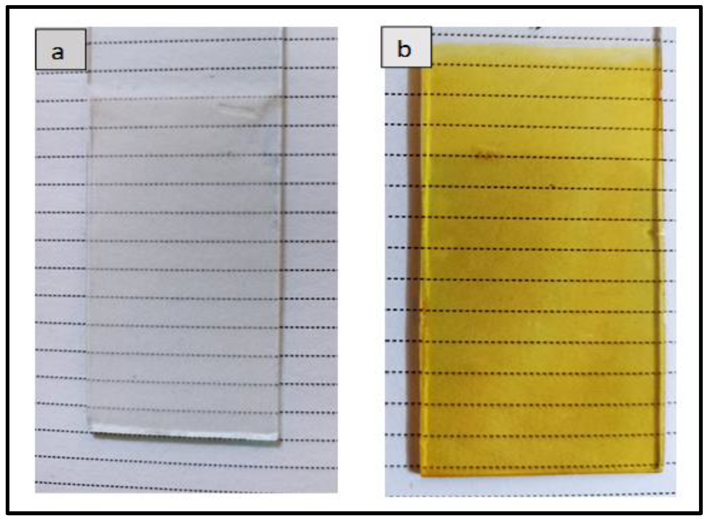
2.3. Deposition of CdO Thin Films

CdO thin films were prepared using 20 mL of CdSO4, an appropriate amount of NH4OH, and H2O2. The volume was completed with distilled water to 100 mL using the CBD technique (Figure 1) in an alkaline solution. The various bath compositions that have been used to prepare solutions are shown in Table 1.
The solution is stirred for a few minutes to obtain a homogeneous mixture. The color of the CBD solution changed from colorless to a white solution at the beginning of NH4OH addition, as shown in Figure 2. With continued addition of the appropriate amount of NH4OH, the solution will return to clear and colorless. The substrates were soaked in the prepared solution at a small angle to the vertical.
The substrates were taken out from the chemical bath at the end of the specified deposition time. It was ultrasonically cleaned with distilled water to remove the precipitated powder layer, then dried in air and kept in a desiccator. After that, the whitish Cd(OH)2 films were annealed at 300 °C in the furnace to convert Cd(OH)2 to CdO thin films through the evaporation of H2O. The whitish films were found to turn brownish, which indicates the formation of CdO thin films as shown in Figure 3.
Thin film thickness (d) was measured using the optical interferometer technique. Which is based on the interference of the reflected light beam from the surface of the film and the bottom of the substrate. He-Ne Laser with a wavelength of 632.8 nm is used. The thickness is measured using the formula:
d = Δ x x · λ 2
where: x is the width of the fringe, Δx is the distance between two fringes, and λ is the wavelength of the laser light [60].
The X-Pert Pro PANalytical X-ray diffraction (XRD) (Malvern Panalytical Ltd., Malvern, UK) was used to investigate the structural properties of the CdO thin films with CuKα radiation with a wavelength of (1.5406 A°) in the 2θ range (10–80°). The surface and morphology properties of the CdO thin films were studied by MIRA 3 TESCAN scanning electron microscopy (SEM) (TESCAN ORSAY HOLDING, a.s., Kohoutovice, Czech Republic). Energy dispersive X-ray diffraction (EDX) (TESCAN ORSAY HOLDING, a.s., Kohoutovice Czech Republic) is linked to the SEM to study the elemental composition. The JENWAY 6850 UV/V (Jenway, Bibby Scientific Ltd, Stone, UK) is spectrophotometer in the range of 300–1100 nm is used to study the optical transmission spectrums of the CdO thin films.
The lattice constant (a) for the cubic structure is calculated using the below relation [61].
a = d h 2 + k 2 + l 2
where (h, k, l) are Miller indices and d the inter planner spacing.
The crystallite size (D) is calculated using the Debye–Scherrer equation [62].
D = 0.9 λ β c o s θ
where (λ) is the wavelength of the X-rays (1.54Å), β is the full width at half-maximum (FWHM) of the peak intensity and θ is the Bragg angle.
The dislocation density (δ) and strain (ε) were determined by Equations (4) and (5), respectively [63,64].
δ = 1 D 2
ε = β c o s θ 4
The number of crystallites per unit area (N) of the films is determined using the relation [62].
N = t D 3
where (t) is the thickness of the films.
The absorption coefficient (α) of thin films was measured using the below equation:
α = 1 d l n ( 1 T )
where d is the thickness and T is the transmittance of the thin film.
The energy band gap (Eg) has been calculated using the Tauc equation:
( α h v ) = A ( h v E g ) n
where A is a constant, hv is the photon energy, and n is an index that takes the values 1/2, 2, 3/2, and 3 for allowed direct, allowed indirect, forbidden direct, and forbidden indirect transition, respectively. In this study, the value of the obtained absorption coefficient is found to be greater than 104 cm−1, which supports the nature of the direct bandgap of the obtained CdO thin films [65].

3. Results and Discussion

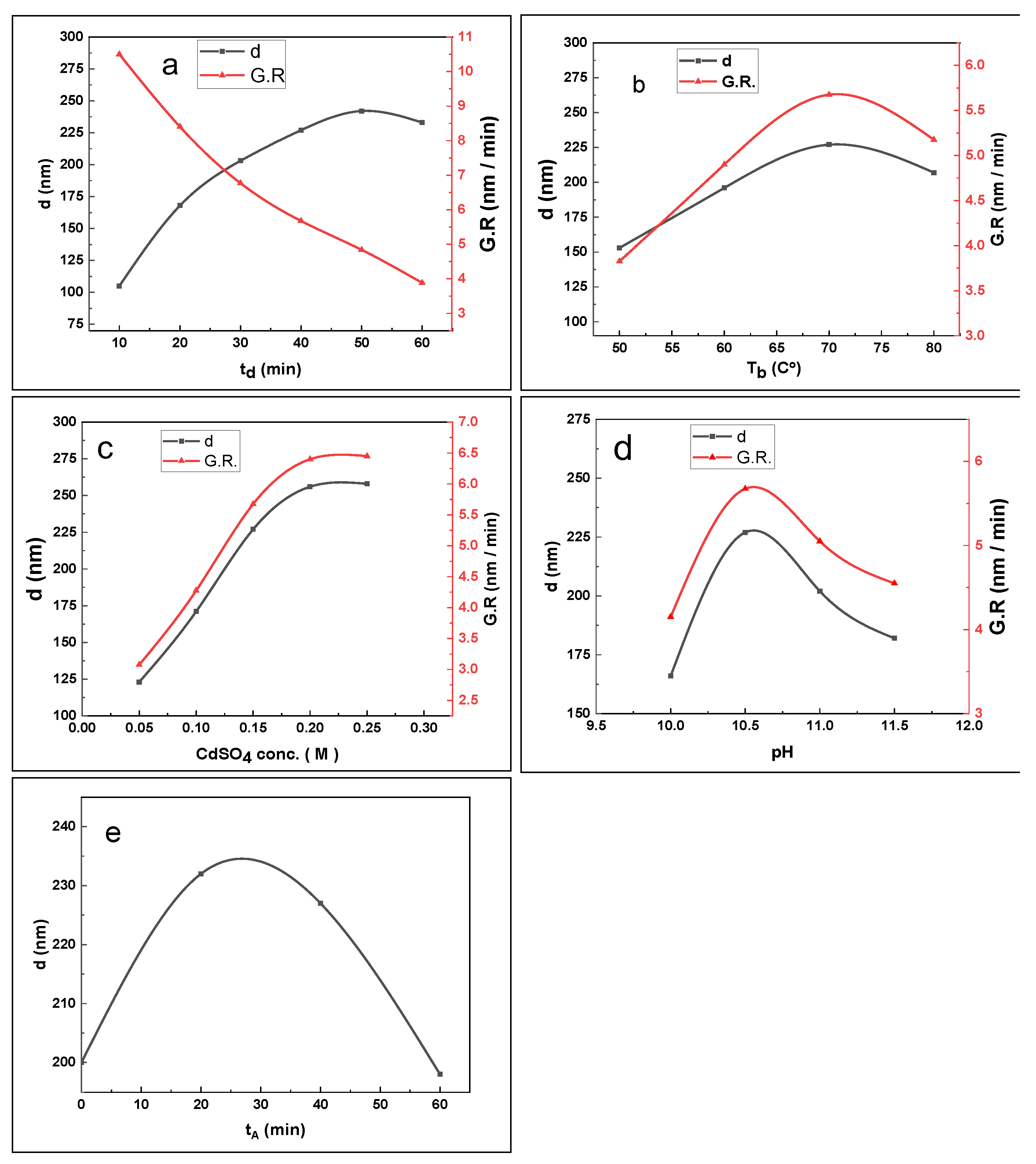
3.1. Thickness and Growth Rate

The formation of Cd(OH)2 layers occurs when the ionic product of Cd2+ and OH exceeds the solubility product of Cd(OH)2 ( Ksp = 7.2 × 10⁻¹⁵ at 25 °C ) [66]. Figure 4 shows the variation of the thickness and growth rate of CdO thin films for different parameters (deposition time, bath temperature, CdSO4 concentration, pH of the bath, and annealing time).
From Figure 4a, it can be seen that there are four stages for the growth of CdO thin films. The first stage is before 10 min, which is known as the initial induction phase, in which no clear growth is observed. This is because the development of the film formation requires the availability of sufficient concentration of Cd2+ ions [67]. The second stage (10–40 min) is known as the main phase, where the change in growth is approximately linear with the deposition time. The thickness of CdO thin films obviously increases with the increase in the deposition time (td) from 10–40 min due to the large growth rate (10.50–5.68 nm/min). The third stage (40–50 min), is known as the termination phase, in which the reaction starts to slow and finally stops. In this stage, the growth rate becomes very small (4.84 nm/min); therefore, a slight increase in thickness is observed, indicating an almost saturated state. This is due to the consumption of the precursor over time [68]. In the fourth stage (50–60 min), a decrement in thickness is observed. This decrement can be attributed to the porous formation of an outer layer and peeling off from the substrate [69]. These results are in good agreement with previous studies reported by Rane YN et al. [70].
Figure 4b shows that the thickness and growth rate of the films increases with the increasing bath temperature (Tb) at a specific deposition time. This is because heating provides the kinetic energy of the ions, which leads to an increase in the number of collisions, and thus the formation of Cd(OH)2, whereas, upon reaching the saturation point at 70 °C, the thickness then starts to decrease when the temperature reaches 80 °C due to the desorption and dissolution of pre-formed Cd(OH)2 [71]. Similar results have been reported by Ahmed HS et al. when investigating the effect of bath temperature on the thickness and growth rate of chemically deposited Cu2S thin films [72].
As shown in Figure 4c, the thickness and growth rate increase from 123 to 256 nm and 3.075 to 6.4 nm/min, respectively, with the increasing CdSO4 concentration from 0.05 to 0.2 M. This is due to the fact that the reaction rate is proportional to the concentration of the reacting ions. In the first stage, when the CdSO4 concentration is low, the number of Cd2+ ions is not enough to combine with all the available OH ions. However, in the second case when the concentration is high, more Cd2+ ions are available, which combine with OH to form Cd(OH)2, which in turn is deposited on the glass substrate and obtains a thin film with a larger thickness [60]. A saturation state was reached with the concentration of 0.25 M. These results were in good agreement with previous results observed by Salunkhe RR et al. [19].
Figure 4d shows that the thickness and growth rate increase with increasing the pH value from 10 to 10.5. As increasing the pH value of the solution means adding more NH4OH, which in turn provides more OH ions that react with Cd2+, thus increasing the reaction rate. However, a decrease in terminal thickness was observed by increasing the pH value of the solution further. This is due to the overly rapid reaction between OH and Cd2+ ions and precipitation of bulk Cd(OH)2 in the solution [73]. These results are in good agreement with the previous study done by Arandhara G et al. [74].
It was found that the optimum deposition parameters are: td = 40 min, Tb = 70 °C, CdSO4 conc. = 0.15 M, and pH = 10.5. The film deposited under these conditions completely covers the surface of the substrate and has good adhesion, which is not removed when wiped or washed with distilled water. The annealing process of the sample under optimum conditions was carried out at 300 °C for different annealing times (tA = 20, 40, 60 min).
Figure 4e shows that the film thickness increases from 200 nm for the as-deposited film to 232 nm by annealing for 20 min despite the evaporation of H2O. This is may be due to the phase change from hexagonal Cd(OH)2 to cubic CdO. However, the thickness of the thin films decreases from 241 to 198 nm when increasing the annealing time from 20 to 60 min, respectively. This is attributed to the progress in the evaporation of H2O molecules, the reduction of grain boundaries with time, and the improvement of the crystal structure of the thin films [75].

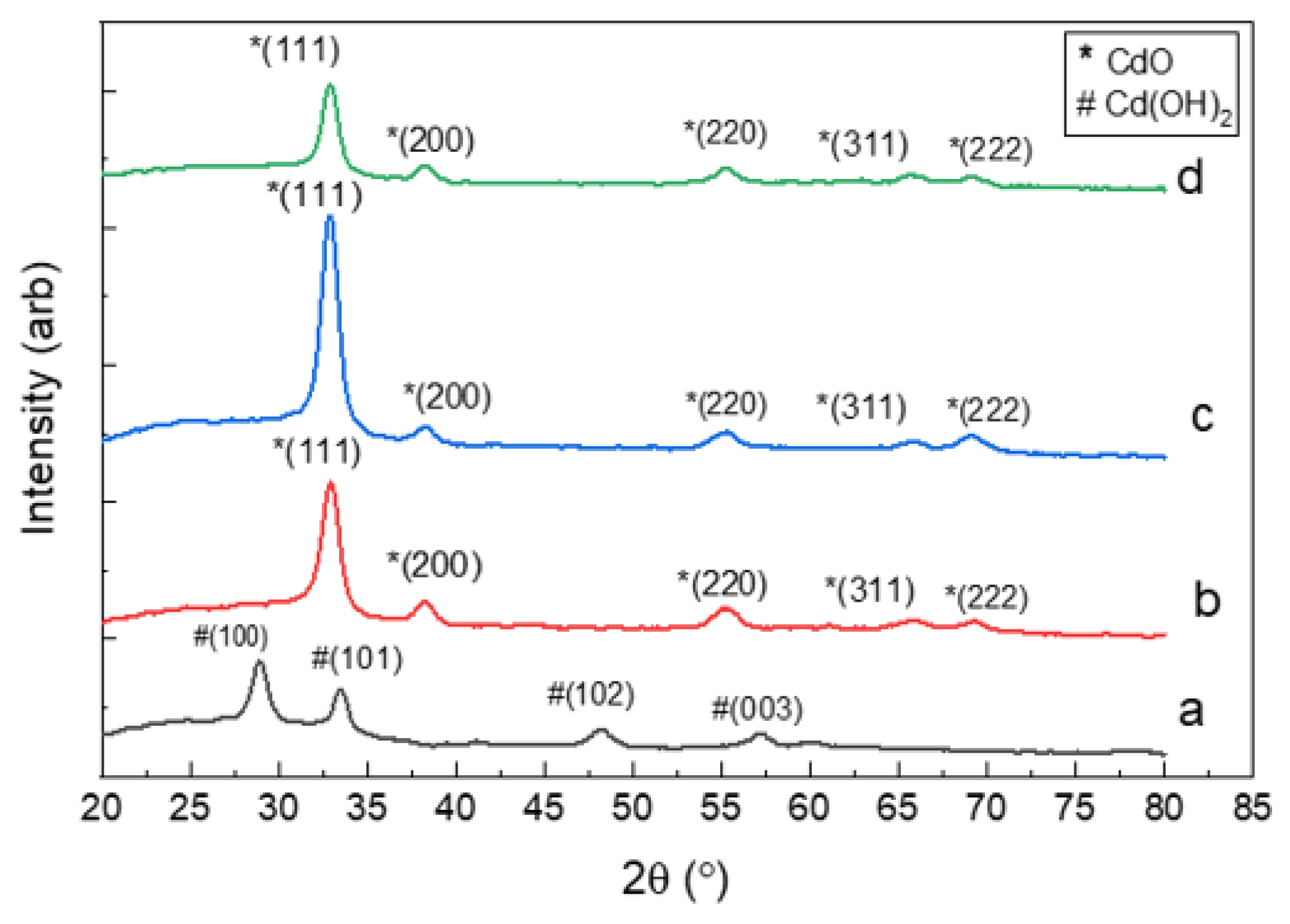
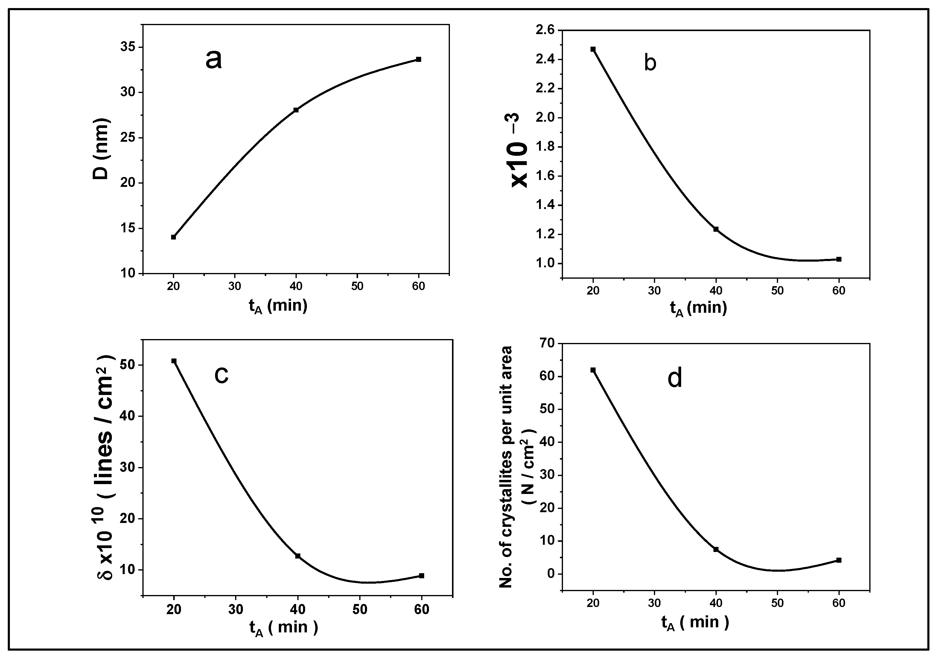
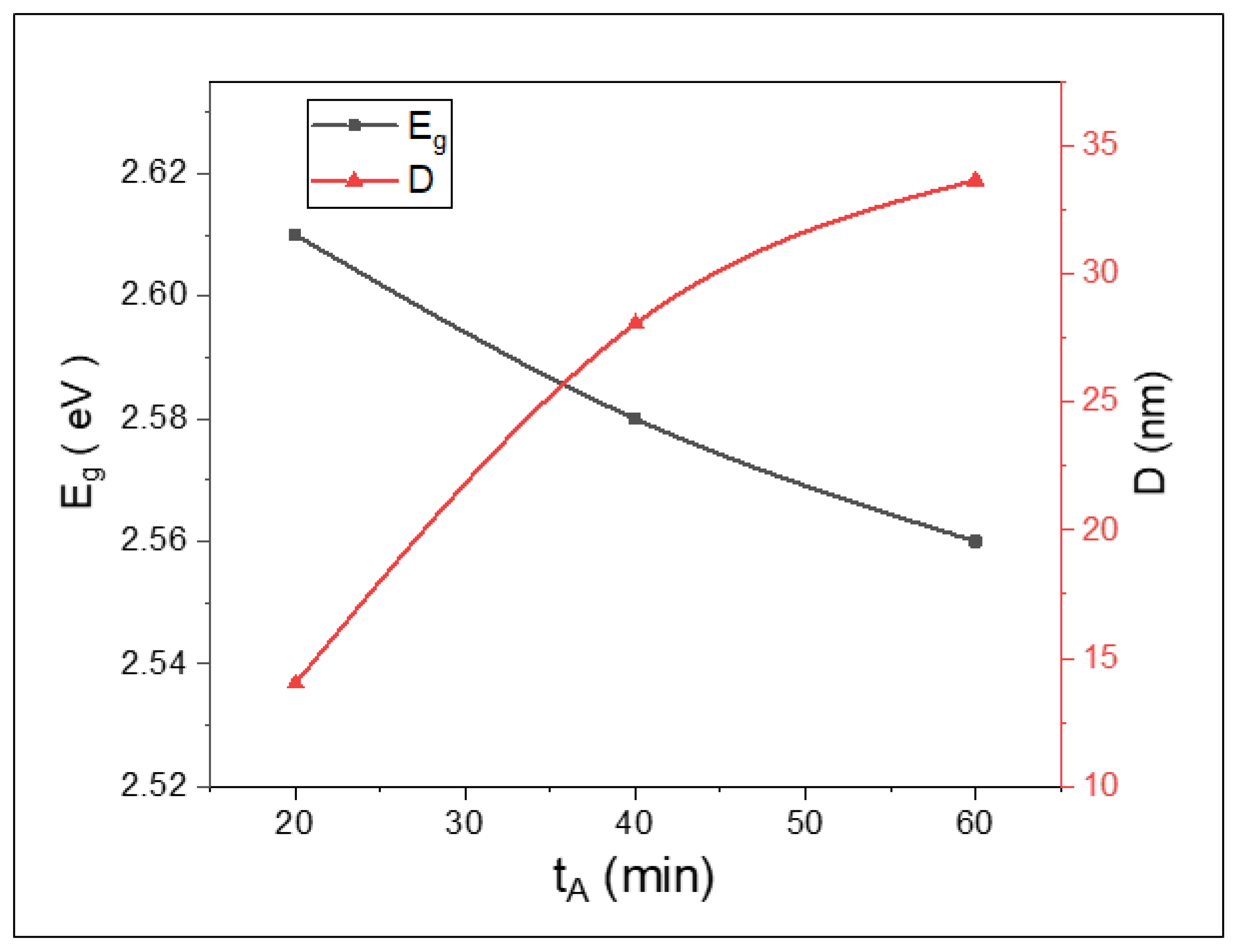
3.2. Structural Properties

Figure 5 represents the XRD patterns of the as-deposited and annealed thin films with different annealing times.
Figure 5a represents the XRD diffraction patterns of the as-deposited thin film, prepared under optimum conditions, showing four peaks at 2θ = 28.945°, 33.524°, 48.184° and 57.243°, which correspond to planes (100), (101), (102), and (003), respectively. All these peaks refer to the hexagonal phase of Cd(OH)2, as compared with the standard data of Cd(OH)2 (JCPDS file no. 31-0228). Similar results were obtained by Ahmed HH [75].
Figure 5b–d represents diffraction patterns for films that have been annealed for 20, 40, and 60 min, respectively, each showing a preferential crystal orientation that corresponds to the diffraction peak (111), which is denoting the prevalent crystal growth along the (111) plane. In addition, four minor peaks refer to planes (200), (220), (311), and (222), which correspond to the angles (2θ) shown in Table 2. These five peaks indicate the cubic polycrystalline phase of CdO compared with the JCPDS file (no. 05-0640). The disappearance of the hexagonal phase of Cd(OH)2 indicates that the H2O has completely evaporated and the film is completely converted to CdO. These observed results are in good agreement with previous studies reported by Ahmed HH, Asmial RA et al., and Jassim SA [75,76].
The diffraction intensity increases with increasing the annealing time from 20 to 40 min. Higher intensity and sharper peaks of the diffraction can be attributed to an increase in the grain size, and an improvement in crystallinity and surface texture, which is useful for photocatalytic activity application [4,30,64]. The decrease in FWHM with increasing annealing time could be due to the grain coalescence at a long annealing time [77]. However, the diffraction intensity began to decrease clearly when the annealing time reached 60 min. The low peak intensity may be due to the small film thickness [73]. It is also observed that the shifting of peaks toward lower values of 2θ with increasing annealing time indicates the decrement in lattice strain [74].
Table 2 shows a comparison between calculated and standard parameters of CdO thin films annealed at different times.
The inter-planner spacing (d) was obtained from the XRD data and found to be consistent with the standard values. The lattice constant (a) has been calculated by Equation (2). A shift in the lattice constant towards it is the standard value (4.695 nm) observed when the film is annealed for 40 min. This indicates an improvement in the quality of the crystalline thin films [76].
The crystallite size (D), dislocation density (δ), strain (ε), and the number of crystallites per unit area (N) have been calculated for the preferential orientation plane (111) using Equations (3)–(6), respectively, and tabulated in Table 3.
The crystallite size is found to be in the range of 14.03–33.65 nm, and it is increased as the annealing time increases, as shown in Figure 6a. This denotes an improvement in the crystallization of the films [74]. From Figure 6b,c, one can see that the strain (ε) and dislocation density (δ) decreased with the increasing annealing time, which indicates a higher degree of crystallization and the increment in grain size (D) of the thin films [78,79].
Moreover, from Table 3, one can see a clear decrement in N with the increasing annealing time. It is decreased from (61.95 to 4.15) × 1011 crystallite/cm2 where the annealing time increased from 20 to 60 min, respectively as shown in Figure 6d. This is attributed to the coalescence of the grains with each other through reducing the number of grain boundaries as the annealing process continues. These results are in agreement with the results previously reported by O. Vigil et al., K. M. Saleh when studying the effect of annealing time on the structural properties of CdO films prepared by spray pyrolysis technique [80,81].
In this work, the most interesting structural properties were obtained at 40 min of annealing time. It was found that the film is peeled off from the substrate when the annealing time reaches 60 min.

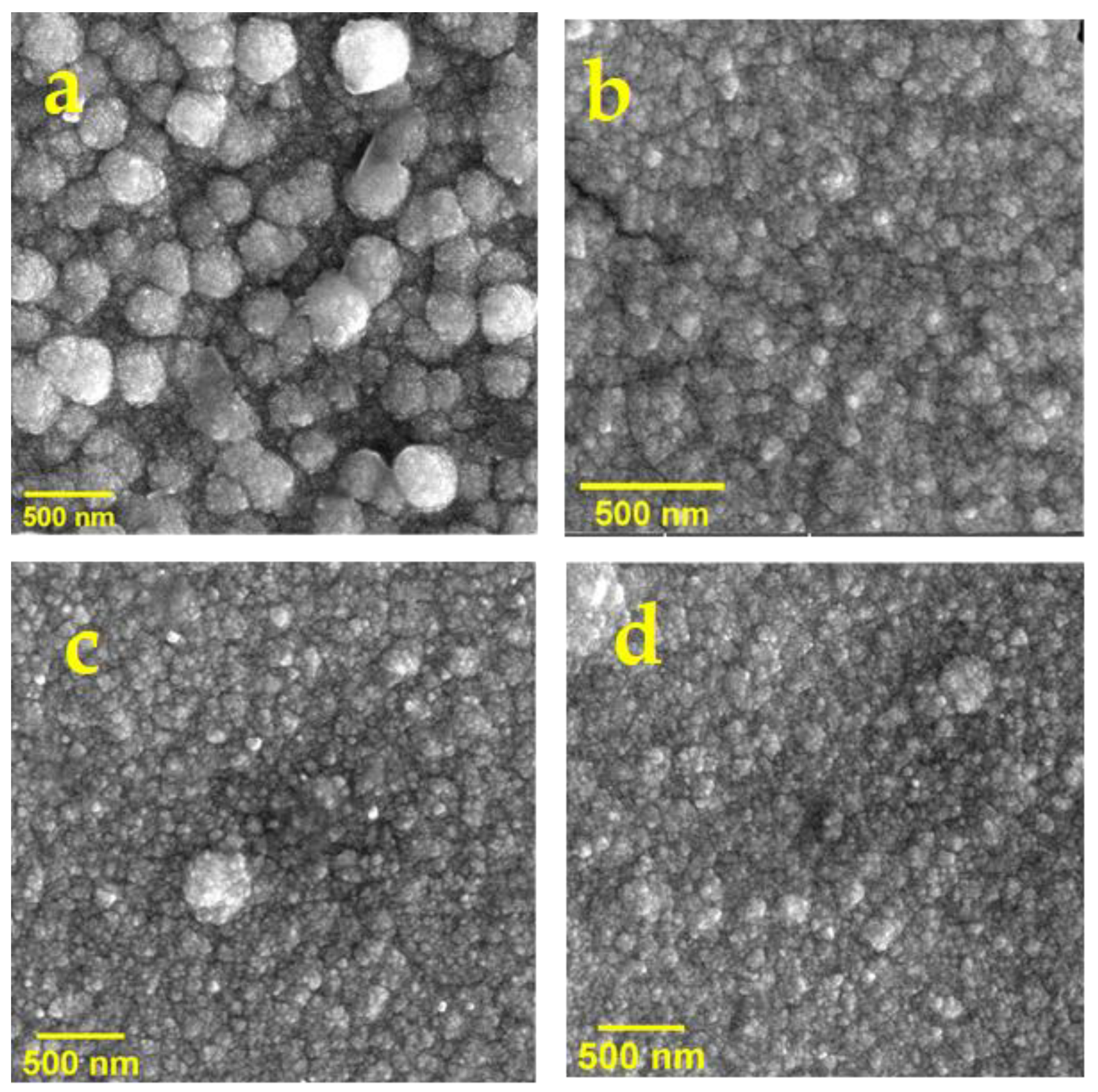
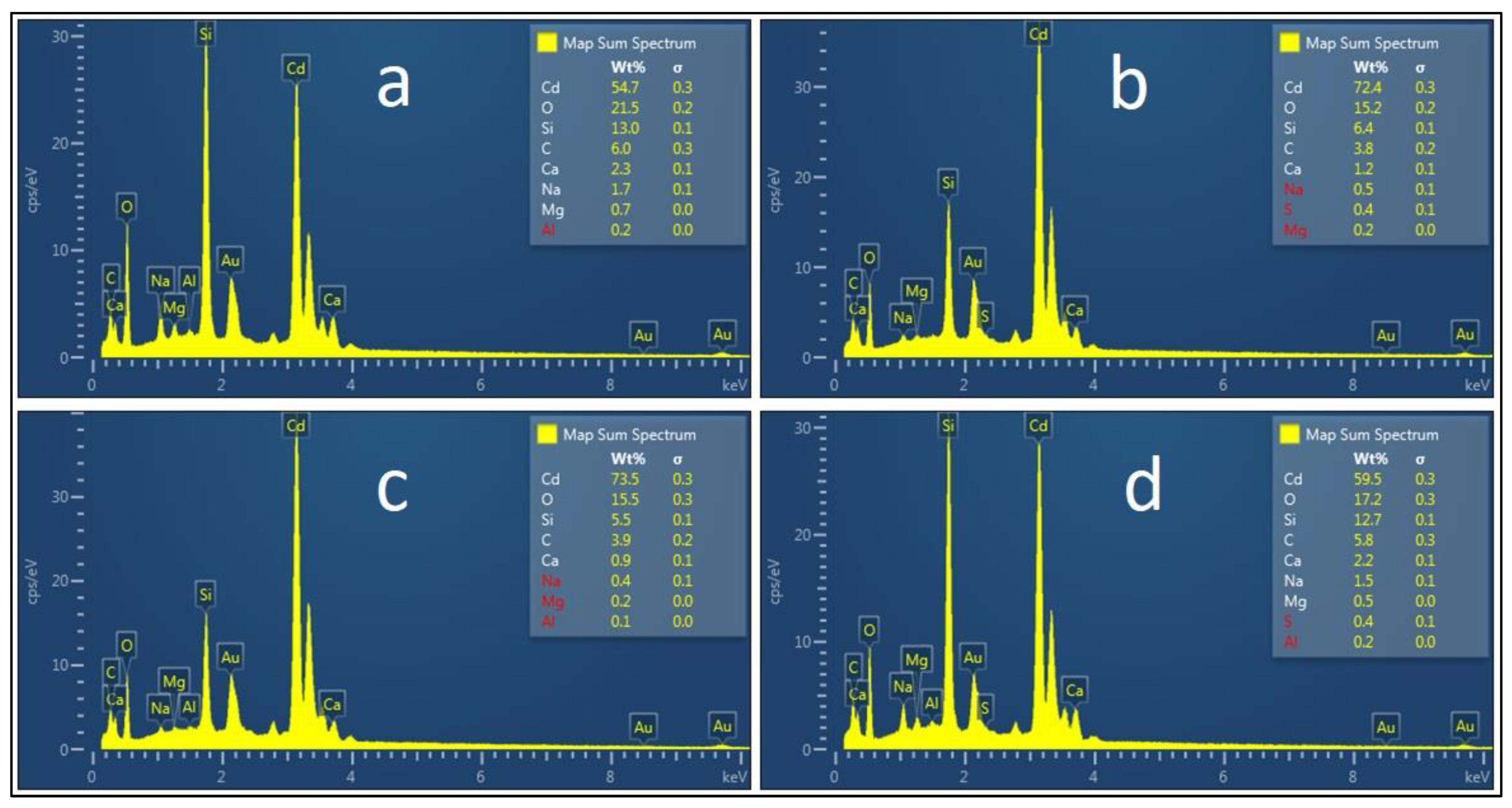
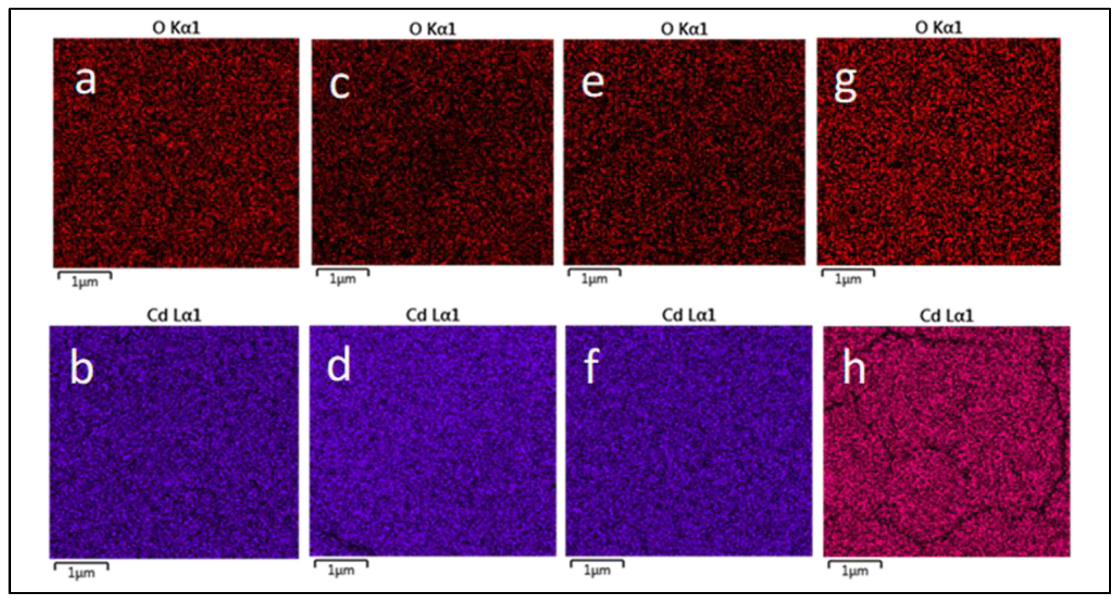
3.3. Morphology and Elementary Composition

Figure 7 shows SEM images of the as-deposited and annealed thin films at different times.
It can be clearly seen that all the thin films consist of spherical-like nanoparticles entirely covering the substrate surface. The morphology appears to be a dense, porous structure in the form of clusters with some cracks appearing in the annealed films. The appearance of cracks may be due to removing the hydroxide phase and/or densification of the CdO thin films during the heat treatment [82,83].
The average particle size is found to be about 243 nm for as-deposited thin films and 80, 59, and 46 nm for annealing times at 20, 40, and 60 min, respectively. the formation of agglomerates was also observed when the annealing time reached 40 min, with the agglomerates increasing with the annealing time increasing to 60 min. The obtained spherical shape with the porous surface and small particle size with the existence of cracks may provide better photocatalytic efficiency due to the increasing reaction surface [21,84].
Figure 8 shows the elemental composition of CdO thin films annealed at different times using EDX.
The analysis confirms the presence of Cd and O in as-deposited and annealed films. The presence of Si, C, Ca, Na, and Mg peaks are attributed to the glass substrate [85]. One can see that the Cd percentage is low in the as-deposited film. The inset of Figure 8 shows that the Cd percentage increased from 54.7% for as-deposited to 72.4% and 73.5% for (20 and 40) min of annealing time, respectively. However, it decreases to 59.5% by peeling the film from the substrate when the annealing time reached 60 min. Inversely, the percentage of O decreases by annealing the films at 20 and 40 min. This is due to the evaporation of the H2O molecule and the transition from the Cd(OH)2 to CdO. These results confirm the XRD results.
Table 4 shows the average atomic ratio of Cd/O as a function of the annealing time. A high percentage of oxygen is observed, which is attributed to the alkaline aqueous solution and/or may be incorporated into the films from the atmosphere during the annealing process [77]. The phenomenon of high concentration of oxygen was also reported previously by (U. T. Nakate et al., A. K. Sharma et al.) [86,87].
Additionally, Figure 9 shows EDX mapping images of the distribution of Cd and O in the films annealed at different times. It can be observed that the Cd and O elements are homogeneously distributed along all the films. The most promising surface morphology and better elemental composition of the CdO thin film were obtained with the annealing time of 40 min.

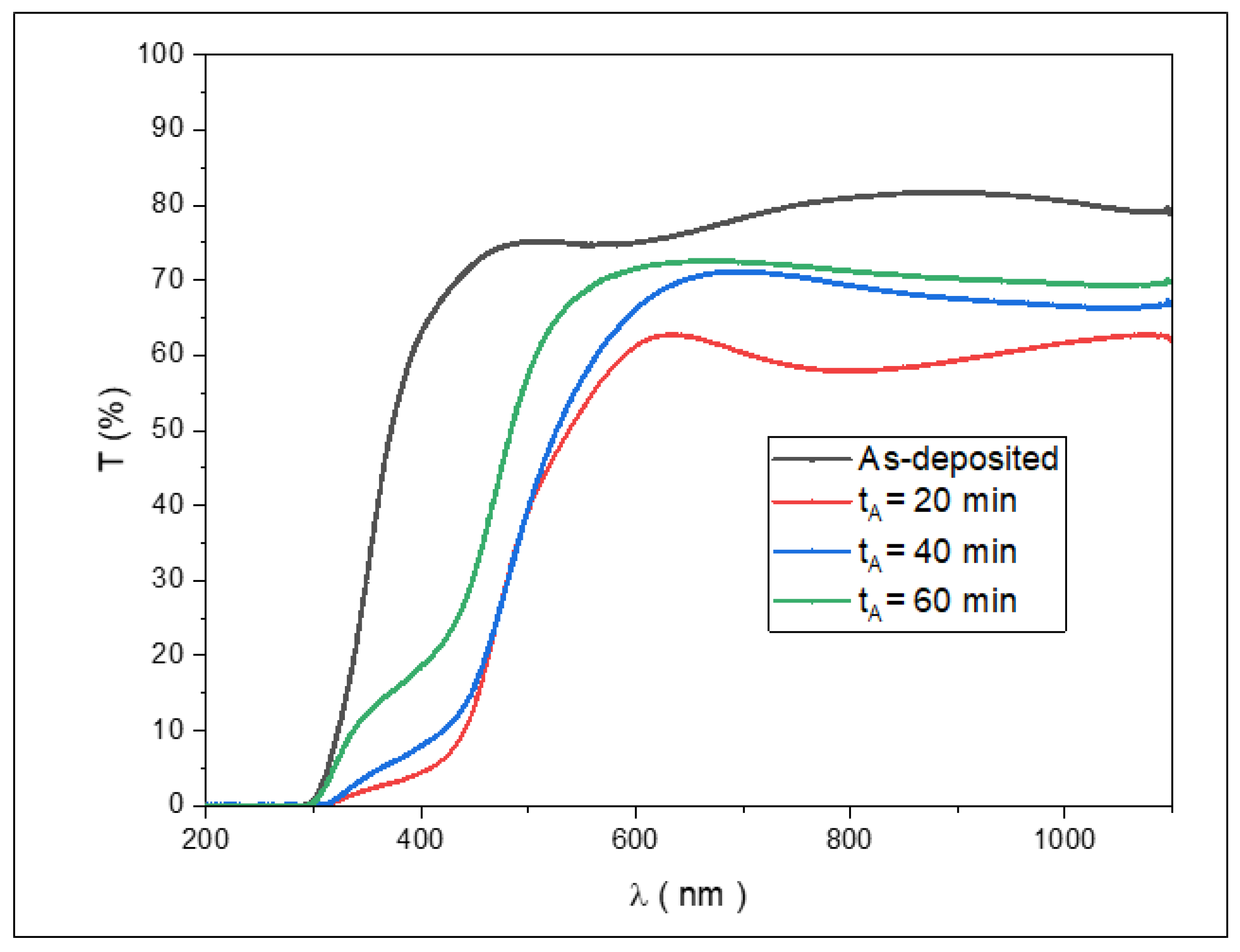
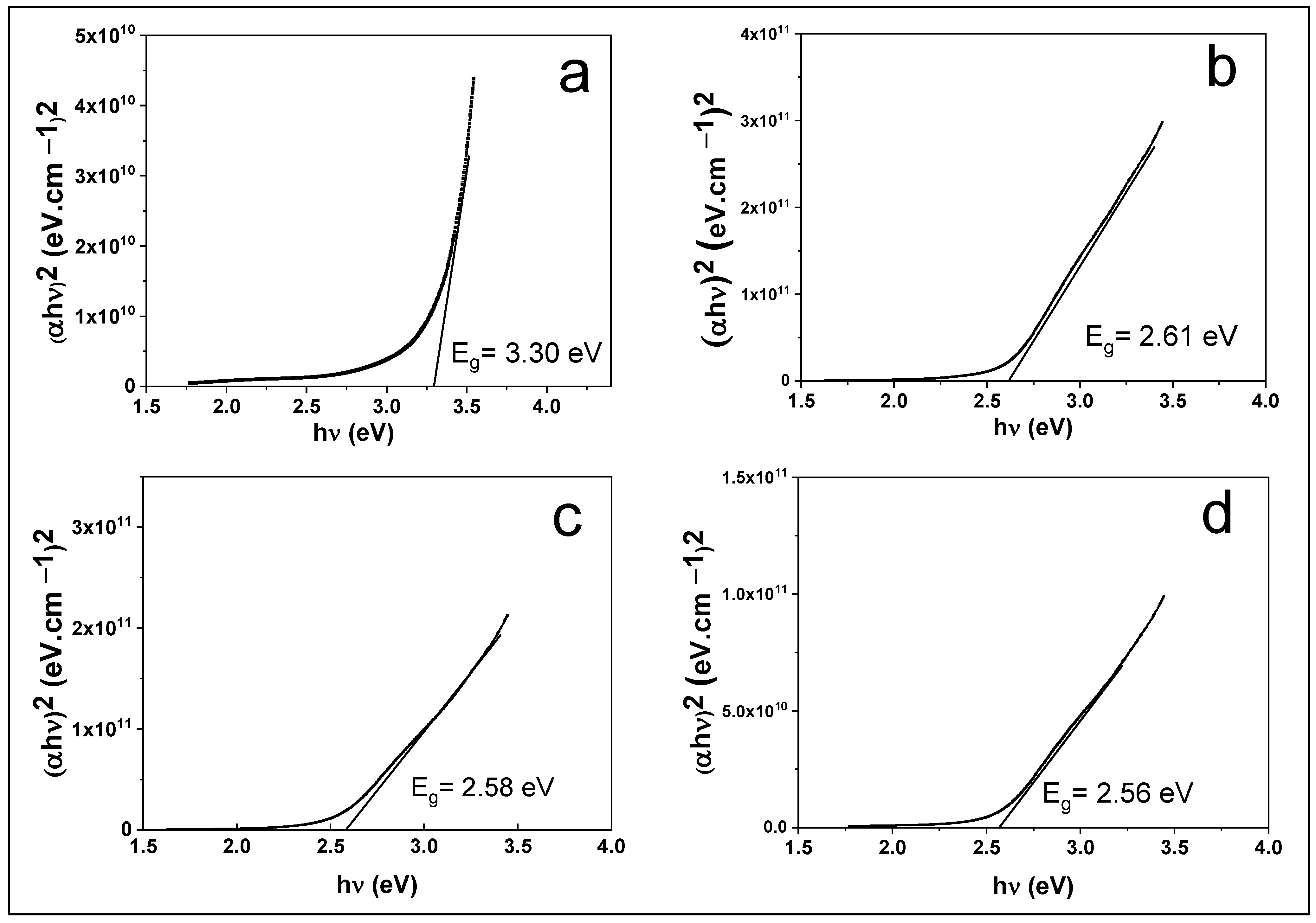
3.4. Optical Properties

Figure 10 shows the optical transmittance (T) spectra for as-deposited and annealed CdO thin films in the range of 300–1100 nm.
It has been found that the transmittance decreases when the film is annealed compared with the as-deposited film. This decrement is due to the increase in thickness during the transition from the hydroxide phase to the oxide phase. The maximum T values of CdO films after the annealing equal 63%, 71%, and 73%, corresponding to annealing times of 20, 40, and 60 min, respectively, in the visible region (625–835 nm). The increase in T with the annealing time is due to the decrease in thickness due to the evaporation of H2O molecules and the increase in crystallite [74,88]. Moreover, the increase in transmittance can be attributed to lower scattering effects due to reducing the crystal defects, structural homogeneity, and crystallinity improvement [89]. In addition, the increase in transmittance may be due to increased carrier concentration and lower bandgap values [79]. These results confirm XRD and EDX results.
To find the energy bandgap Eg, the absorption coefficient (α) was calculated from Equation (8). The band gap was determined by plotting a graph between (αhv)2 and (hv). The energy bandgap was estimated through the extrapolation of the linear portion of the curve to (hv) at zero (αhv)2 and is shown in Figure 11 [90].
Figure 12 shows the variation of Eg under different annealing times.
It is found that the Eg of the as-deposited thin film is 3.30 eV, which is matched with a previously reported value for Cd(OH)2 thin film Eg (3.2–3.5 eV) [55]. However, Eg decreases from 2.61–2.56 eV when increasing the annealing time from 20 to 60 min, respectively. This is due to the increase in the crystallite size and crystallinity improvement [91]. The decrease in the Eg could be due to the increased oxygen content of the film due to the annealing process [79]. Some defects such as vacancies and atoms adsorbed on crystal surfaces, etc., if some of their energy levels in the bandgap are close to the lower part of the conduction band, the absorption associated with these defects will cause a reduction in the absorption of CdO, resulting in a decrement in the bandgap value [92].
Moreover, the calculation of the band gap from the Tauc diagram is considered the most convenient method for calculating the energy gap in much of the literature; however, there is an error rate of about 0.03 as the maximum, depending on the technique and accuracy of drawing the tangent line [92,93]. The results confirm XRD and EDX results. These results are in agreement with the results previously reported by (A. A. P. Frit et al., V. Soliya et al., and A. Bouraiou et al.) when studied the effect of annealing time on the optical properties of other thin films prepared by different methods [94,95,96].

4. Conclusions

Nanostructured CdO thin films were successfully deposited by the CBD technique. It has been observed that the deposition parameters strongly affected the thickness, growth rate, and quality of CdO thin films. It has been observed that the thickness increased with increasing the deposition time and bath temperature from 10 to 50 min, and 50 to 70 °C, respectively. After that, the thickness starts to decrease as the deposition time and bath temperature reach 60 min and 80 °C, respectively. Additionally, the thickness increased with increasing CdSO4 concentration from 0.05 to 0.25 M. The growth rate was found to decrease with the deposition time and increases with the bath temperature and precursor concentration. Moreover, the thickness and growth rate increased with increasing pH from 10 to 10.5. However, they started decreasing as the pH value reached 11. Furthermore, it was found that the thickness of thin films decreases with increasing the annealing time. It is noteworthy that the saturation state was observed only in the case of precursor concentration.
It was found that the optimum deposition parameters are: deposition time 40 min, bath temperature 70 °C, CdSO4 concentration 0.15 M, and pH value 10.5. Additionally, the best film quality is obtained at 40 min of annealing time.
XRD showed a hexagonal phase of polycrystalline Cd(OH)2 for as-deposited thin films. However, all the annealed films are polycrystalline CdO with a cubic face and a preferential orientation (111). The peak intensity and crystallite size were found to increase with annealing time. However, the FWHM, strain, dislocation density, and the number of crystallites were found to be decreased with the annealing time.
SEM images of annealed films showed homogeneous surfaces in the form of spherical nanoparticles with an average particle size of 80–46 nm. It decreased with the annealing time, and the agglomerated nanoparticles increased as the annealing time increased. EDX analysis revealed that the best atomic stoichiometry of Cd/O was obtained at 40 min of annealing time.
Optical analysis shows that the transmittance of CdO thin films increases and the energy gap decreases when increasing the annealing time.

Author Contributions

Conceptualization, R.Y.M.; methodology, R.Y.M.; software, K.R.K.; validation, R.Y.M. and K.R.K.; formal analysis, R.Y.M.; investigation, R.Y.M.; resources, R.Y.M.; data curation, K.R.K.; writing—original draft preparation, K.R.K.; writing—review and editing, R.Y.M.; visualization, R.Y.M. and K.R.K.; supervision, R.Y.M.; project administration, R.Y.M.; funding acquisition, University of Duhok. All authors have read and agreed to the published version of the manuscript.

Funding

This research was funded by the University of Duhok.

Acknowledgments

The acknowledgment is directed to the University of Duhok for their support.

Conflicts of Interest

First the authors declare no conflict of interest. Second, the funders had no role in the design of the study; in the collection, analyses, or interpretation of data; in the writing of the manuscript, or in the decision to publish the results.

References

  1. Jadduaa, M.H.; Harbi, Z.A.; Habubi, N.F. The Effect of Substrate Temperature on the Band Transition, Cauchy Dispersion and Urbach Energy of Nanostructure CdO Thin Films. Int. Lett. Chem. Phys. Astron. 2015, 58, 83–89. [Google Scholar] [CrossRef]
  2. Jassim, S.A.-J.; Nassar, E.M.A. Effect of annealing temperature on structure and optical properties of CdO nanocrystaline thin film prepare by chemical bath deposition method. IOP Conf. Ser. Mater. Sci. Eng. 2020, 928, 072046. [Google Scholar] [CrossRef]
  3. Habubi, N.F.; Abrahim, B.A.; Noore, E.S. Influence of Irradiation on some Optical Properties of (CdO) Thin Films Prepared by Spray Pyrolysis. Int. Lett. Chem. Phys. Astron. 2017, 74, 15–21. [Google Scholar] [CrossRef]
  4. Thambidurai, M.; Dang, C. Structural, morphological and optical properties of CdO nanostructures synthesized by chemical bath deposition method. Mater. Lett. 2018, 221, 244–247. [Google Scholar] [CrossRef]
  5. Jassim, S.A.-J.; Nassar, E.M.A. Effect of deposition time on the structure, direct and indirect energy gap of nanoparticles CdO thin films deposited by chemical bath deposition technique. J. Phys. Conf. Ser. 2021, 1879, 032106. [Google Scholar] [CrossRef]
  6. Aldeen, T.S.; Mohamed, H.E.A.; Maaza, M. Bio-inspired Single Phase Monteponite CdO Nanoparticles via Natural Extract of Phoenix roebelenii Palm Leaves. J. Inorg. Organomet. Polym. Mater. 2020, 30, 4691–4701. [Google Scholar] [CrossRef]
  7. Zaien, M. Growth of cadmium oxide nanorods by vapor transport. Chalcogenide Lett. 2012, 9, 115–119. [Google Scholar]
  8. Şahin, B. Physical properties of nanostructured CdO films from alkaline baths containing saccharin as additive. Sci. World J. 2013, 2013, 1–5. [Google Scholar] [CrossRef] [PubMed]
  9. Ranjan, M.; Partha, D. SILAR—Synthesized CdO thin films for improved supercapacitive, photocatalytic and LPG—Sensing performance. Chem. Pap. 2019, 73, 1605–1619. [Google Scholar]
  10. Shameem, A.; Devendran, P.; Siva, V.; Raja, M.; Bahadur, S.A.; Manikandan, A. Preparation and Characterization Studies of Nanostructured CdO Thin Films by SILAR Method for Photocatalytic Applications. J. Inorg. Organomet. Polym. Mater. 2017, 27, 692–699. [Google Scholar] [CrossRef]
  11. Dakhel, A.A. Structural, optical and electrical measurements on boron-doped CdO thin films. J. Mater. Sci. 2011, 46, 6925–6931. [Google Scholar] [CrossRef]
  12. Santana, G.; Morales-Acevedo, A.; Vigil, O.; Vaillant, L.; Cruz, F.; Contreras-Puente, G. Structural and optical properties of (ZnO)x (CdO)1-X thin films obtained by spray pyrolysis. Thin Solid Films 2000, 373, 235–238. [Google Scholar] [CrossRef]
  13. Hames, Y.; San, S.E. CdO/Cu2O solar cells by chemical deposition. Sol. Energy 2004, 77, 291–294. [Google Scholar] [CrossRef]
  14. Ismail, R.A.; Abdulrazaq, O.A. A new route for fabricating CdO/c-Si heterojunction solar cells. Sol. Energy Mater. Sol. Cells 2007, 91, 903–907. [Google Scholar] [CrossRef]
  15. Gozeh, B.A.; Karabulut, A.; Ismael, C.B.; Saleh, S.I.; Yakuphanoglu, F. Zn-doped CdO effects on the optical, electrical and photoresponse properties of heterojunctions-based photodiodes. J. Alloys Compd. 2021, 872, 159624. [Google Scholar] [CrossRef]
  16. Dugan, S.; Koç, M.M.; Coşkun, B. Structural, electrical and optical characterization of Mn doped CdO photodiodes. J. Mol. Struct. 2020, 1202, 127235. [Google Scholar] [CrossRef]
  17. Ortega, M.; Santana, G.; Morales-Acevedo, A. Optoelectronic properties of CdO/Si photodetectors. Solid-State Electron. 2000, 44, 1765–1769. [Google Scholar] [CrossRef]
  18. Kamble, A.; Pawar, R.; Patil, J.; Suryavanshi, S.; Patil, P. From nanowires to cubes of CdO: Ethanol gas response. J. Alloys Compd. 2011, 509, 1035–1039. [Google Scholar] [CrossRef]
  19. Salunkhe, R.; Shinde, V.; Lokhande, C. Liquefied petroleum gas (LPG) sensing properties of nanocrystalline CdO thin films prepared by chemical route: Effect of molarities of precursor solution. Sens. Actuators B Chem. 2008, 133, 296–301. [Google Scholar] [CrossRef]
  20. Reddy, C.V.; Babu, B.; Shim, J. Synthesis, optical properties and efficient photocatalytic activity of CdO/ZnO hybrid nanocomposite. J. Phys. Chem. Solids 2018, 112, 20–28. [Google Scholar] [CrossRef]
  21. Millesi, S.; Schilirò, M.; Greco, F.; Crupi, I.; Impellizzeri, G.; Priolo, F.; Egdell, R.G.; Gulino, A. Nanostructured CdO thin films for water treatments. Mater. Sci. Semicond. Processing 2016, 42, 85–88. [Google Scholar] [CrossRef]
  22. Hussein, B.H.; Hassun, H.K.; Maiyaly, B.K.; Aleabi, S.H. Effect of copper on physical properties of CdO thin films and n-CdO: Cu/p-Si heterojunction. J. Ovonic Res. 2022, 18, 37–42. [Google Scholar] [CrossRef]
  23. Aydoğu, H.S.; Çabuk, G.; Çoban, M.B. The effects of different Ga doping on structural, optical and electrical properties of CdO films. Süleyman Demirel Üniv. Fen Bilimleri Enst. Derg. 2019, 23, 140–147. [Google Scholar]
  24. Thirumoorthi, M.; Prakash, J.T.J. A study of Tin doping effects on physical properties of CdO thin films prepared by sol–gel spin coating method. J. Asian Ceram. Soc. 2016, 4, 39–45. [Google Scholar] [CrossRef]
  25. Zaien, M.; Ahmed, N.; Hassan, Z. Effects of annealing on the optical and electrical properties of CdO thin films prepared by thermal evaporation. Mater. Lett. 2013, 105, 84–86. [Google Scholar] [CrossRef]
  26. Purohit, A.; Chander, S.; Dhaka, M. Impact of annealing on physical properties of e-beam evaporated polycrystalline CdO thin films for optoelectronic applications. Opt. Mater. 2017, 66, 512–518. [Google Scholar] [CrossRef]
  27. Menazea, A.; Mostafa, A.M.; Al-Ashkar, E.A. Impact of CuO doping on the properties of CdO thin films on the catalytic degradation by using pulsed-Laser deposition technique. Opt. Mater. 2020, 100, 109663. [Google Scholar] [CrossRef]
  28. Hymavathi, B.; Kumar, B.R.; Rao, T.S. ScienceDirect Investigations on Physical Properties of Nanostructured Cr doped CdO Thin Films Prepared by DC Reactive Magnetron Sputtering. Procedia Mater. Sci. 2017, 4, 7867–7874. [Google Scholar]
  29. Saha, B.; Thapa, R.; Chattopadhyay, K.K. Wide range tuning of electrical conductivity of RF sputtered CdO thin films through oxygen partial pressure variation. Sol. Energy Mater. Sol. Cells 2008, 92, 1077–1080. [Google Scholar] [CrossRef]
  30. Gokul, B.; Matheswaran, P.; Sathyamoorthy, R. Influence of Annealing on Physical Properties of CdO Thin Films Prepared by SILAR Method. J. Mater. Sci. Technol. 2013, 29, 17–21. [Google Scholar] [CrossRef]
  31. Rahman, M.A.; Khan, M.K.R. Effect of annealing temperature on structural, electrical and optical properties of spray pyrolytic nanocrystalline CdO thin films. Mater. Sci. Semicond. Processing 2014, 24, 26–33. [Google Scholar] [CrossRef]
  32. Yakuphanoglu, F. Nanocluster n-CdO thin film by sol-gel for solar cell applications. Appl. Surf. Sci. 2010, 257, 1413–1419. [Google Scholar] [CrossRef]
  33. Hone, F.G.; Tegegne, N.A.; Dejene, F.B.; Andoshe, D.M. Nanofiber Cadmium oxide thin films Prepared from Ethanolamine Complexing agent by Solution growth method. Optik 2021, 243, 167402. [Google Scholar] [CrossRef]
  34. Lavate, D.; Sawant, V.; Khomane, A. Photodegradation of Rhodamine-B Dye under Natural Sunlight using CdO. Bull. Chem. React. Eng. Catal. 2022, 17, 466–475. [Google Scholar] [CrossRef]
  35. Ahmad, F.; Devade, S.K. Investigation of the Optical Band Gap Energy of Cadmium Oxide (CDO) Nanostructured Thin Film. Int. Res. J. Mod. Eng. Technol. Sci. 2022, 4, 4014–4017. [Google Scholar]
  36. Mondal, S. Structural and optical properties of CBD synthesised CdO thin films: Influence of Ni incorporation. Adv. Mater. Process. Technol. 2021, 1–8. [Google Scholar] [CrossRef]
  37. Das, M.R.; Mukherjee, A.; Mitra, P. Structural, optical and electrical characterization of CBD synthesized CdO thin films: Influence of deposition time. Mater. Sci. 2017, 35, 470–478. [Google Scholar] [CrossRef]
  38. Hone, F.G.; Abza, T. Short review of factors affecting chemical bath deposition method for metal chalcogenide thin films. Int. J. Thin. Film Sci. Technol. 2019, 8, 43–52. [Google Scholar]
  39. Verma, A.K.; Dash, R.R.; Bhunia, P. A review on chemical coagulation/flocculation technologies for removal of colour from textile wastewaters. J. Environ. Manag. 2012, 93, 154–168. [Google Scholar] [CrossRef]
  40. Rahimi, R.; Kerdari, H.; Rabbani, M.; Shafiee, M. Synthesis, characterization and adsorbing properties of hollow Zn-Fe2O4 nanospheres on removal of Congo red from aqueous solution. Desalination 2011, 280, 412–418. [Google Scholar] [CrossRef]
  41. Afkhami, A.; Moosavi, R. Adsorptive removal of Congo red, a carcinogenic textile dye, from aqueous solutions by maghemite nanoparticles. J. Hazard. Mater. 2010, 174, 398–403. [Google Scholar] [CrossRef] [PubMed]
  42. Hung, S.-T.; Chang, C.-J.; Hsu, M.-H. Improved photocatalytic performance of ZnO nanograss decorated pore-array films by surface texture modification and silver nanoparticle deposition. J. Hazard. Mater. 2011, 198, 307–316. [Google Scholar] [CrossRef] [PubMed]
  43. Di Paola, A.; García-López, E.; Marcì, G.; Palmisano, L. A survey of photocatalytic materials for environmental remediation. J. Hazard. Mater. 2012, 211, 3–29. [Google Scholar] [CrossRef] [PubMed]
  44. Huang, M.; Xu, C.; Wu, Z.; Huang, Y.; Lin, J.; Wu, J. Photocatalytic discolorization of methyl orange solution by Pt modified TiO2 loaded on natural zeolite. Dye. Pigment. 2008, 77, 327–334. [Google Scholar] [CrossRef]
  45. Fernández, J.; Kiwi, J.; Baeza, J.; Freer, J.; Lizama, C.; Mansilla, H. Orange II photocatalysis on immobilised TiO2: Effect of the pH and H2O2. Appl. Catal. B Environ. 2004, 48, 205–211. [Google Scholar] [CrossRef]
  46. Baruah, S.; Pal, S.K.; Dutta, J. Nanostructured Zinc Oxide for Water Treatment. Nanosci. Nanotechnol. Asia 2012, 2, 90–102. [Google Scholar] [CrossRef] [Green Version]
  47. Abdollahi, Y.; Abdullah, A.H.; Zainal, Z.; Yusof, N.A. Photocatalytic Degradation of p-Cresol by Zinc Oxide under UV Irradiation. Int. J. Mol. Sci. 2011, 13, 302–315. [Google Scholar] [CrossRef] [PubMed]
  48. Peternel, I.T.; Koprivanac, N.; Bozic, A.L.; Kušić, H.M. Comparative study of UV/TiO2, UV/ZnO and photo-Fenton processes for the organic reactive dye degradation in aqueous solution. J. Hazard. Mater. 2007, 148, 477–484. [Google Scholar] [CrossRef]
  49. Sathishkumar, P.; Mangalaraja, R.V.; Rozas, O.; Mansilla, H.D.; Gracia-Pinilla, M.; Anandan, S. Low frequency ultrasound (42 kHz) assisted degradation of Acid Blue 113 in the presence of visible light driven rare earth nanoclusters loaded TiO2 nanophotocatalysts. Ultrason. Sonochem. 2014, 21, 1675–1681. [Google Scholar] [CrossRef] [PubMed]
  50. Yousef, A.; Barakat, N.A.M.; Amna, T.; Unnithan, A.R.; Al-Deyab, S.S.; Kim, H.Y. Influence of CdO-doping on the photoluminescence properties of ZnO nanofibers: Effective visible light photocatalyst for waste water treatment. J. Lumin. 2012, 132, 1668–1677. [Google Scholar] [CrossRef]
  51. Tadjarodi, A.; Imani, M.; Kerdari, H. Experimental design to optimize the synthesis of CdO cauliflower-like nanostructure and high performance in photodegradation of toxic azo dyes. Mater. Res. Bull. 2013, 48, 935–942. [Google Scholar] [CrossRef]
  52. Gujar, T.; Shinde, V.; Kim, W.-Y.; Jung, K.-D.; Lokhande, C.; Joo, O.-S. Formation of CdO films from chemically deposited Cd(OH)2 films as a precursor. Appl. Surf. Sci. 2008, 254, 3813–3818. [Google Scholar] [CrossRef]
  53. Karbovnyk, I.; Bolesta, I.; Rovetskyi, I.; Lesivtsiv, V.; Shmygelsky, Y.; Velgosh, S.; Popov, A.I. Long-term evolution of luminescent properties in CdI2 crystals. Low Temp. Phys. 2016, 42, 594–596. [Google Scholar] [CrossRef]
  54. Ghoshal, T.; Kar, S. Morphology controlled solvothermal synthesis of Cd(OH)2 and CdO micro/nanocrystals on Cd foil. Appl. Surf. Sci. 2009, 255, 8091–8097. [Google Scholar] [CrossRef]
  55. Mane, R.; Han, S.-H. Growth of limited quantum dot chains of cadmium hydroxide thin films by chemical route. Electrochem. Commun. 2005, 7, 205–208. [Google Scholar] [CrossRef]
  56. Adnan, J.; Arfan, M.; Shahid, T.; Khan, M.; Masab, R.; Ramish, A.; Ahtasham, S.; Wattoo, A.; Hashim, M.; Zahoor, A.; et al. Synthesis of cadmium hydroxide nanostructure via composite-hydroxide-mediated approach. Nanomater. Nanotechnol. 2019, 9, 1847980419852551. [Google Scholar] [CrossRef]
  57. Sahin, B.; Bayansal, F.; Çakmak, H.; Kahraman, S.; Çetinkara, H. Effect of heat treatment on the properties of Cd(OH)2 and CdO films grown by chemical bath deposition. Philos. Mag. Lett. 2013, 93, 101–108. [Google Scholar] [CrossRef]
  58. Ahmed, S.M.; Mohammed, R.Y.; Abdulrahman, A.F.; Ahmed, F.K.; Hamad, S.M. Synthesis and characterization of lead oxide nanostructures for radiation attenuation application. Mater. Sci. Semicond. Process. 2021, 130, 105830. [Google Scholar] [CrossRef]
  59. Mohammed, R.Y.; Ilyas, B.M. Comparative study of chemically deposited CdS thin films and of the non-synthesized CdSO4 under pressure and temperature within first principles. Mater. Today Commun. 2020, 25, 101518. [Google Scholar] [CrossRef]
  60. Mohammed, K.A.; Ahmed, S.M.; Mohammed, R.Y.; Mohammed, K. Investigation of Structure, Optical, and Electrical Properties of CuS Thin Films by CBD Technique. Crystals 2020, 10, 684. [Google Scholar] [CrossRef]
  61. Sakthivel, P.; Murugan, R.; Asaithambi, S.; Karuppaiah, M.; Rajendran, S.; Ravi, G. Radio frequency magnetron sputtered CdO thin films for optoelectronic applications. J. Phys. Chem. Solids 2019, 126, 1–10. [Google Scholar] [CrossRef]
  62. Mohammed, R.Y.; Abduol, S.; Mousa, A.M. Structural and Optical Properties of Chemically Deposited CdS Thin Films. Int. Lett. Chem. Phys. Astron. 2014, 29, 91–104. [Google Scholar] [CrossRef]
  63. Elttayef, A.-H.K.; Ajeel, H.M.; Khudiar, A.I. Effect of annealing temperature and doping with Cu on physical properties of cadmium oxide thin films. J. Mater. Res. Technol. 2013, 2, 182–187. [Google Scholar] [CrossRef]
  64. Ravikumar, M.; Chandramohan, R.; Valanarasu, S.; Manogowri, R.; Kathalingam, A. Substrate temperature dependent opto-electronic properties of perfume atomized CdO thin films. Inorg. Nano-Metal Chem. 2017, 47, 1495–1500. [Google Scholar] [CrossRef]
  65. Ullah, H.; Rahaman, R.; Mahmud, S. Optical Properties of Cadmium Oxide (CdO) Thin Films. Indones. J. Electr. Eng. Comput. Sci. 2017, 5, 81–84. [Google Scholar] [CrossRef]
  66. Luis, F.; Moncayo, G. CRC Handbook of Chemistry and Physics, 97th ed.; CRC Press: Boca Raton, FL, USA, 2017; pp. 5–177. [Google Scholar]
  67. Hodes, G. Semiconductor and ceramic nanoparticle films deposited by chemical bath deposition. Phys. Chem. Chem. Phys. 2007, 9, 2181–2196. [Google Scholar] [CrossRef]
  68. Ahmed, H.S.; Mohammed, R.Y.; Khalil, M.H. Effects of Deposition Time and PH on The Characterization of Chemically Synthesized Composite Nano-Wires of Cu2S Thin Films. Sci. J. Univ. Zakho 2021, 9, 184–192. [Google Scholar] [CrossRef]
  69. Shinde, M.S.; Ahirrao, P.B.; Patil, I.J.; Patil, R.S. Thickness dependent electrical and optical properties of nanocrystalline copper sulphide thin films grown by simple chemical route. Indian J. Pure Appl. Phys. 2012, 50, 657–660. [Google Scholar]
  70. Rane, Y.; Shende, D.; Raghuwanshi, M.; Koli, R.; Gosavi, S.; Deshpande, N. Visible-light assisted CdO nanowires photocatalyst for toxic dye degradation studies. Optik 2018, 179, 535–544. [Google Scholar] [CrossRef]
  71. Ouachtari, F.; Rmili, A.; Elidrissi, B.; Bouaoud, A.; Erguig, H.; Elies, P. Influence of Bath Temperature, Deposition Time and S/Cd Ratio on the Structure, Surface Morphology, Chemical Composition and Optical Properties of CdS Thin Films Elaborated by Chemical Bath Deposition. J. Mod. Phys. 2011, 02, 1073–1082. [Google Scholar] [CrossRef]
  72. Ahmed, H.S.; Mohammed, R.Y. The Effect of Deposition Parameters on Morphological and Optical Properties of Cu2S Thin Films Grown by Chemical Bath Deposition Technique. Photonics 2022, 9, 161. [Google Scholar] [CrossRef]
  73. Ismail, R.A.; Ahmed, H.H.; Al-Samarai, A.E.; Mohmed, S.J. Effect of pH on the structural and optical properties of nanostructured CdO films grown by chemical bath deposition technique. Micro Nano Lett. 2014, 9, 935–939. [Google Scholar] [CrossRef]
  74. Arandhara, G.; Bora, J.; Saikia, P. Effect of pH on the crystallite size, elastic properties and morphology of nanostructured ZnS thin films prepared by chemical bath deposition technique. Mater. Chem. Phys. 2020, 241, 122277. [Google Scholar] [CrossRef]
  75. Ahmed, H.H. Variation of the structural, optical and electrical properties of CBD CdO with processing temperature. Mater. Sci. Semicond. Process. 2017, 66, 215–222. [Google Scholar] [CrossRef]
  76. Asmial, R.A.; Al-Samarai, A.-M.E.; Mohmed, S.J.; Ahmed, H.H. Characteristics of Nanostructured CdO Films Prepared by Chemical Bath Deposition Technique. Int. J. Mod. Phys. B 2012, 26, 1250135. [Google Scholar] [CrossRef]
  77. Bhunia, A.K.; Pradhan, S.S.; Saha, S. Effect of Annealing Time on the Optical and Structural Properties of ZnO Nanorods. J. Nano-Electron. Phys. 2019, 11, 06003. [Google Scholar]
  78. Nwanya, A.; Chigbo, C.; Ezugwu, S.; Osuji, R.; Malik, M.; Ezema, F. Transformation of cadmium hydroxide to cadmium oxide thin films synthesized by SILAR deposition process: Role of varying deposition cycles. J. Assoc. Arab Univ. Basic Appl. Sci. 2016, 20, 49–54. [Google Scholar] [CrossRef]
  79. Chandramohan, R.; Vijayan, T.; Arumugam, S.; Ramalingam, H.; Dhanasekaran, V.; Sundaram, K.; Mahalingam, T. Effect of heat treatment on microstructural and optical properties of CBD grown Al-doped ZnO thin films. Mater. Sci. Eng. B 2011, 176, 152–156. [Google Scholar] [CrossRef]
  80. Vigil, O.; Cruz-Gandarilla, F.; Morales-Acevedo, A.; Contreras-Puente, G.; Vaillant, L.; Santana, G. Structural and optical properties of annealed CdO thin films prepared by spray pyrolysis. Mater. Chem. Phys. 2001, 68, 249–252. [Google Scholar] [CrossRef]
  81. Saleh, K.M. Study the Structural Properties and Surface Morphology of CdO Thin Films Prepared by Chemical Spray pyrolysis Karrar. J. Kufa-Phys. 2020, 12, 1–11. [Google Scholar] [CrossRef]
  82. Gujar, T.; Shinde, V.; Lokhande, C.; Mane, R.; Han, S.-H. Bismuth oxide thin films prepared by chemical bath deposition (CBD) method: Annealing effect. Appl. Surf. Sci. 2005, 250, 161–167. [Google Scholar] [CrossRef]
  83. Islam, M.; Hossain, M.; Aliyu, M.; Chelvanathan, P.; Huda, Q.; Karim, M.; Sopian, K.; Amin, N. Comparison of Structural and Optical Properties of CdS Thin Films Grown by CSVT, CBD and Sputtering Techniques. Energy Procedia 2013, 33, 203–213. [Google Scholar] [CrossRef]
  84. Jiang, Y. Synthesis and Characterization of Photocatalytic PVA/TiO2 Nanoparticulate Thin Films Materials Science and Engineering. Doctoral Dissertation, UNSW Sydney, Sydney, NSW, Australia, 2019. [Google Scholar]
  85. Cortes, A.; Gómez, H.; Marotti, R.E.; Riveros, G.; Dalchiele, E.A. Grain size dependence of the bandgap in chemical bath deposited CdS thin films. Sol. Energy Mater. Sol. Cells 2004, 82, 21–34. [Google Scholar] [CrossRef]
  86. Nakate, U.T.; Patil, P.; Ghule, B.; Nakate, Y.T.; Ekar, S.; Ambare, R.C.; Mane, R. Room temperature LPG sensing properties using spray pyrolysis deposited nano-crystalline CdO thin films. Surfaces Interfaces 2019, 17, 100339. [Google Scholar] [CrossRef]
  87. Sharma, A.; Potdar, S.; Yewale, M.; Shirgaonkar, D.B.; Pakhare, K.; Sargar, B.; Rokade, M.; Patil, U. Influence of bath temperature on microstructure and NH3 sensing properties of chemically synthesized CdO thin films. Mater. Sci. 2019, 37, 25–32. [Google Scholar] [CrossRef]
  88. Şahin, B.; Taşköprü, T.; Bayansal, F. Bandgap variation of nanostructure tin doped CdO films via SILAR processing. Ceram Int. 2014, 40, 8709–8714. [Google Scholar] [CrossRef]
  89. Usharani, K.; Balu, A.R. Properties of spray deposited Zn, Mg incorporated CdO thin films. J. Mater. Sci. Mater. Electron. 2016, 27, 2071–2078. [Google Scholar] [CrossRef]
  90. Mohammad, J.; Al-jumaili, H. Effect of Time and Temperature Variation on Chemical Bath Deposition Nanocrystalline CdS Thin Film. J. Coll. Educ. 2013, 5. Available online: https://www.researchgate.net/publication/310510318_Effect_of_Time_and_Temperature_Variation_on_Chemical_Bath_Deposition_Nanocrystalline_CdS_Thin_Film (accessed on 1 August 2022).
  91. Hile, D.; Swart, H.; Motloung, S.; Pawade, V.; Kroon, R.; Egbo, K.; Koao, L. Phase transformation on zinc selenide thin films deposited by photo-assisted chemical bath method: The effect of annealing temperature. Mater. Sci. Semicond. Process. 2020, 115, 105118. [Google Scholar] [CrossRef]
  92. Brik, M.; Srivastava, A.; Popov, A. A few common misconceptions in the interpretation of experimental spectroscopic data. Opt. Mater. 2022, 127, 112276. [Google Scholar] [CrossRef]
  93. Jubu, P.R.; Yam, F.K.; Igba, V.M.; Beh, K.P. Tauc-plot scale and extrapolation effect on bandgap estimation from UV–vis–NIR data—A case study of β-Ga2O3. J. Solid. State Chem. 2020, 290, 121576. [Google Scholar] [CrossRef]
  94. Frit, A.A.P.; Deepalakshmi, K.; Prithivikumaran, N.; Jeyakumaran, N. The effect of annealing time on lead oxide thin films coated on indium tin oxide substrate. Int. J. ChemTech Res. 2014, 6, 5347–5352. [Google Scholar]
  95. Soliya, V.; Tandel, D.; Patel, C.; Patel, K. Effect of annealing time on optical and electrical properties of CdS thin films. In AIP Conference Proceedings; AIP Publishing LLC: Melville, NY, USA, 2018; Volume 1961, p. 030025. [Google Scholar] [CrossRef]
  96. Bouraiou, A.; Aida, M.; Mosbah, A.; Attaf, N. Annealing time effect on the properties of CuInSe2 grown by electrodeposition using two electrodes system. Braz. J. Phys. 2009, 39, 543–546. [Google Scholar] [CrossRef] [Green Version]
Figure 1. Experimental setup of CBD technique.
Crystals 12 01315 g001
Figure 2. Different stages of chemical bath solution where (a) aqueous solution of CdSO4, (b) immediately upon adding 1 mL of NH4OH, (c) after adding the appropriate amount of NH4OH, (d) after adding H2O2 and distilled water, and (e) after 3–5 min of heating to 50 °C.
Crystals 12 01315 g002
Figure 3. The photography images of thin films: (a) before, and (b) after the annealing process.
Crystals 12 01315 g003
Figure 4. The variation of thickness and growth rate of CdO thin films with (a) deposition time, (b) bath temperature, (c) CdSO4 concentration, (d) pH of the bath, and (e) annealing time.
Crystals 12 01315 g004
Figure 5. XRD patterns of as-deposited and annealed thin films where t (a) = (b) 20 min, (c) 40 min, and (d) 60 min.
Crystals 12 01315 g005
Figure 6. Variation of structural values with annealing time. (a) Crystallite size, (b) strain, (c) dislocation density, and (d) the number of crystallites per unit area.
Crystals 12 01315 g006
Figure 7. SEM photographs for (a) as-deposited, and annealed thin films at (b) 20 min, (c) 40 min, and (d) 60 min.
Crystals 12 01315 g007
Figure 8. EDX of as-deposited and annealed thin films at different annealing times. (a) As-deposited, (b) 20 min, (c) 40 min, and (d) 60 min.
Crystals 12 01315 g008
Figure 9. EDX mapping analysis of Cd and O elements with various annealing times: (a,b) as-deposited, (c,d) 20 min,(e,f) 40 min, and (g,h) 60 min.
Crystals 12 01315 g009
Figure 10. Transmittance spectra of as-deposited and annealed thin films at different times.
Crystals 12 01315 g010
Figure 11. The energy gap of as-deposited and annealed thin films where: (a) as-deposited, (b) 20 min, (c) 40 min, and (d) 60 min.
Crystals 12 01315 g011
Figure 12. Variation of energy gap as a function of annealing time and crystallite size.
Crystals 12 01315 g012
Table 1. Chemical bath compositions.
Bath No.12345
CdSO4 conc.(M)0.150.150.05–0.25
By step 0.05
0.150.15
pH10.510.510.510–11.5
By step 0.5
10.5
td (min)10–60
By step 10
40404040
Tb(°C)7050–80
By step 10
707070
Table 2. The observed and standard values of some XRD parameters for CdO thin films.
tA (min)hklObserved 2θ (°)Standard 2θ (°)Observed d (Å)Standard d (Å)Observed a (Å)Observed I (%)Standard I (%)
2011132.92433.022.7202.7124.712100100
20038.32438.2862.3482.3494.69717.9488
22055.19355.2601.6641.6614.70812.9143
31165.88265.9121.4171.4164.7027.5728
22269.29669.2901.3551.3554.6937.6913
4011133.04133.022.7112.7124.696100100
20038.31138.2862.3492.3494.6999.3688
22055.30355.2601.6611.6614.6987.7043
31165.78665.9121.4191.4164.7084.7828
22269.15969.2901.3571.3554.7027.9713
6011132.80933.022.7292.7124.728100100
20038.25438.2862.3522.3494.70614.8488
22055.36155.2601.6591.6614.69417.6543
31165.75065.9121.4201.4164.71110.7328
22269.31069.2901.3551.3554.6938.8113
Table 3. Calculated values of the structural parameters of CdO thin films at different annealing times.
tA (min)2θ (°)FWHM β (2θ°)Grain Size, D (nm)Micro Strain, ε (×10−3)Dislocation Density, δ × 1010 (Lines/cm2)N/Unit Area (×1011 Crystallites/cm2)
2032.9240.590414.0252.47150.83561.95
4033.0410.295228.0591.23512.70110.28
6032.8090.246033.6511.0298.8314.15
Table 4. Compositional analysis of CdO thin films at different annealing times.
Annealing Time (min)Cd Atomic %O Atomic %Cd/O
As-deposited16.4445.50.36
2028.1942.940.66
4029.9444.060.68
6019.5939.770.5
Publisher’s Note: MDPI stays neutral with regard to jurisdictional claims in published maps and institutional affiliations.

