Article

Effect of Gate Dielectric Material on the Electrical Properties of MoSe2-Based Metal–Insulator–Semiconductor Field-Effect Transistor

Department of Electrical Engineering, Chosun University, 375, Seosuk-dong, Dong-gu, Gwangju 501-759, Korea
*
Author to whom correspondence should be addressed.
These authors contributed equally to this work.
Crystals 2022, 12(9), 1301; https://doi.org/10.3390/cryst12091301
Submission received: 26 August 2022 / Revised: 8 September 2022 / Accepted: 12 September 2022 / Published: 14 September 2022

Abstract

:
In this study, we fabricated metal–insulator–semiconductor field-effect transistors (MISFETs) based on nanolayered molybdenum diselenide (MoSe2) using two insulator materials, silicon dioxide (SiO2) and silicon nitride (SiN). We performed morphological and electrical characterizations in which the devices showed good electronic performance, such as high mobility and high Ion/Ioff ratios exceeding 104. The subthreshold swing (ss) was somewhat high in all devices owing to the dimensions of our devices. In addition, the transfer curves showed good controllability as a function of gate voltage. The photogating effect was weakened in MoSe2/SiN/Si, indicating that SiN is a good alternative to silicon oxide as a gate dielectric material.

1. Introduction

Two-dimensional (2D) transition metal dichalcogenides (TMDCs) have attracted considerable attention because of their unique electronic [1], photonic [2], electrochemical [3], and mechanical [4] properties, which are significant advantages for the fabrication of next-generation electronic and optoelectronic devices [5]. Scaling down electronic device dimensions, in particular field-effect transistors (FETs) including metal–insulator–semiconductor field-effect transistors (MISFETs), is challenging owing to Moore’s law, because the reduction in the channel size and in the thickness of the gate dielectric material cause short channel effects and increases in leakage current, respectively [6]. Moreover, devices with reduced dimensions require decreased power consumption; in other words, a low threshold voltage is necessary to achieve the best electronic performance [7]. Therefore, selecting a gate dielectric material with the best physical properties, such as a high dielectric constant and low mismatch with the channel material, is as important as selecting the 2D active layer in FET-based devices. We previously reported the investigation of van der Waals hexagonal boron nitride (h-BN) (indirect bandgap Eg = 5.955 eV [8] and dielectric constant ε = 3.3 [9]) as an alternative gate dielectric material; however, the results showed low electrical performance and a kink effect due to carrier trapping at the interface between h-BN and molybdenum diselenide (MoSe2) [10]. MoSe2-based FETs have been reported to have excellent device characteristics, such as an on/off ratio of 106 and Hall mobilities exceeding 250 cm2/V·s for both holes and electrons [11].
In this paper, we report the fabrication and characterization of MoSe2-based MISFET transistors using silicon dioxide (SiO2) and silicon nitride (SiN) as gate dielectric materials. The aim of our research is to investigate the incorporation of SiN, which is a high-κ dielectric material [12] (with a dielectric constant ε = 7.5, almost two times higher than that of SiO2, ε = 3.9), as an insulator layer. We used the same fabrication process and device properties (i.e., device size, active-layer thickness, dielectric material thickness, etc.). The electrical characteristics of the MISFET devices were determined, and their mobilities, subthreshold swing (ss) values, and other parameters were calculated and analyzed.

2. Materials and Methods

We used two types of substrates in this study: SiO2/Si and SiN/Si substrates using p+-doped Si with a resistivity lower than 0.005 Ω·cm. The thicknesses of the SiO2 and SiN were 300 nm. SiN (300 nm) was deposited using low-pressure chemical vapor deposition (LPCVD). Thereafter, Ti contacts with thicknesses of 50 nm were deposited by electron-beam evaporation. Then, nanolayered MoSe2 flakes purchased from HQ Graphene were transferred onto the SiO2/Si and SiN/Si substrates using polydimethylsiloxane (PDMS, Sylgard 184 Dow silicones corporation, Carrollton, KY, USA). Four devices were fabricated on the SiO2/Si substrates using MoSe2 flake thicknesses of 7, 21, 63, and 90 nm, and another four devices were fabricated on SiN/Si with MoSe2 flake thicknesses of 29, 36, 47, and 87 nm. Finally, the MISFET devices were annealed at 400 °C for 2 h under Ar gas and atmospheric pressure. A semiconductor parameter analyzer (4155A, Hewlett Packard, Tokyo, Japan) and probe station were used for electrical characterization. Scanning electron microscopy (SEM, Hitachi, Jena, Germany) was used to observe the surface of the MoSe2 flakes, and the thickness of MoSe2 was determined using atomic force microscopy (AFM, XE-200, PSIA Corp., Seoul, Korea).

3. Results and Discussion

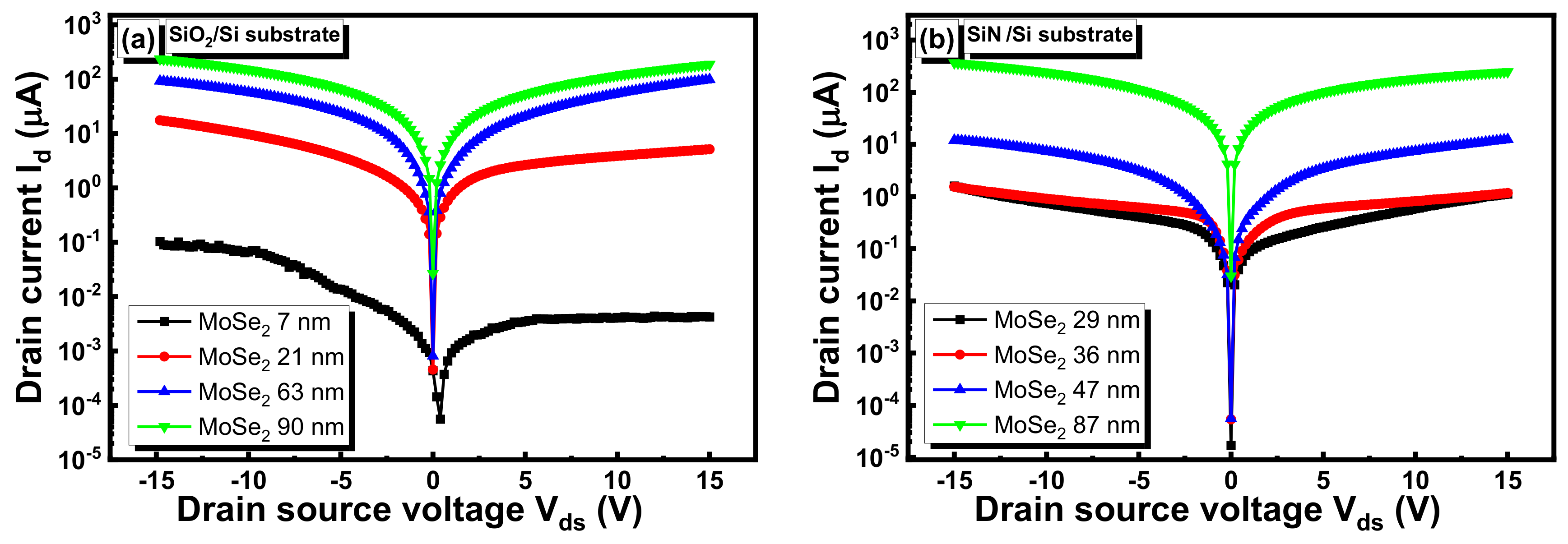
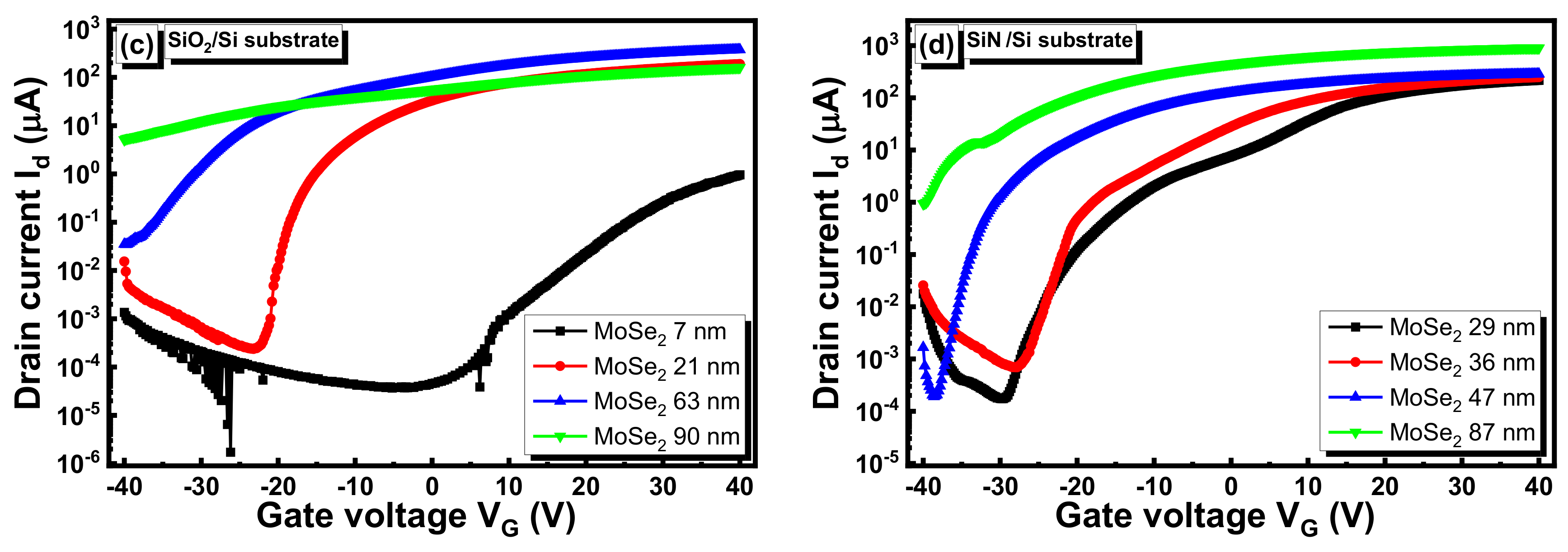
3.1. Electrical Characterization of All Samples

Figure 1a,b show the drain current (Id) dependence on the drain–source voltage (Vds) curves of the MISFETs fabricated on SiO2/Si and SiN/Si substrates, respectively. All devices showed symmetric electrical characteristics, except for the device using the thinnest MoSe2 layer (7 nm) on SiO2/Si because of the high electrical resistivity of the layer. Figure 1c,d depict the transfer curves of the same devices. All devices showed n-type behavior with normal turn-on behavior. The devices with thinner MoSe2 flakes exhibited poor transfer curves. The electrical properties of all eight devices were extracted from the transfer curves and are presented in Table 1. In general, the devices showed good electrical properties, with the highest carrier mobility in MoSe2/SiN/Si with the MoSe2 thickness of 87 nm; this device also showed a high on/off ratio exceeding 104. The ss values were relatively lower in the MoSe2/SiN/Si-based devices, indicating that using SiN as a gate dielectric material enhanced the electrical properties.
As shown in Table 1, MoSe2/SiO2/Si with the MoSe2 thickness of 21 nm and MoSe2/SiN/Si with the MoSe2 thickness of 29 nm had similar electrical properties; these were chosen for further investigation to determine the best gate dielectric material. The field-effect mobilities ( μ eff ) of the devices were estimated using the equation μ eff = dI d / dV g × L / WC i V ds , where C i is the gate capacitance calculated using the equation C i = ε 0 ε r / d ; and ε r is equal to 7.5 and 3.9, respectively, in the cases of SiN and SiO2. The thicknesses of the SiN and SiO2 were 300 nm, the gate capacitances were 1.15 × 10⁻⁴ and 2.21 × 10⁻⁴ F·m−2, and L and W were the channel length and width, respectively.

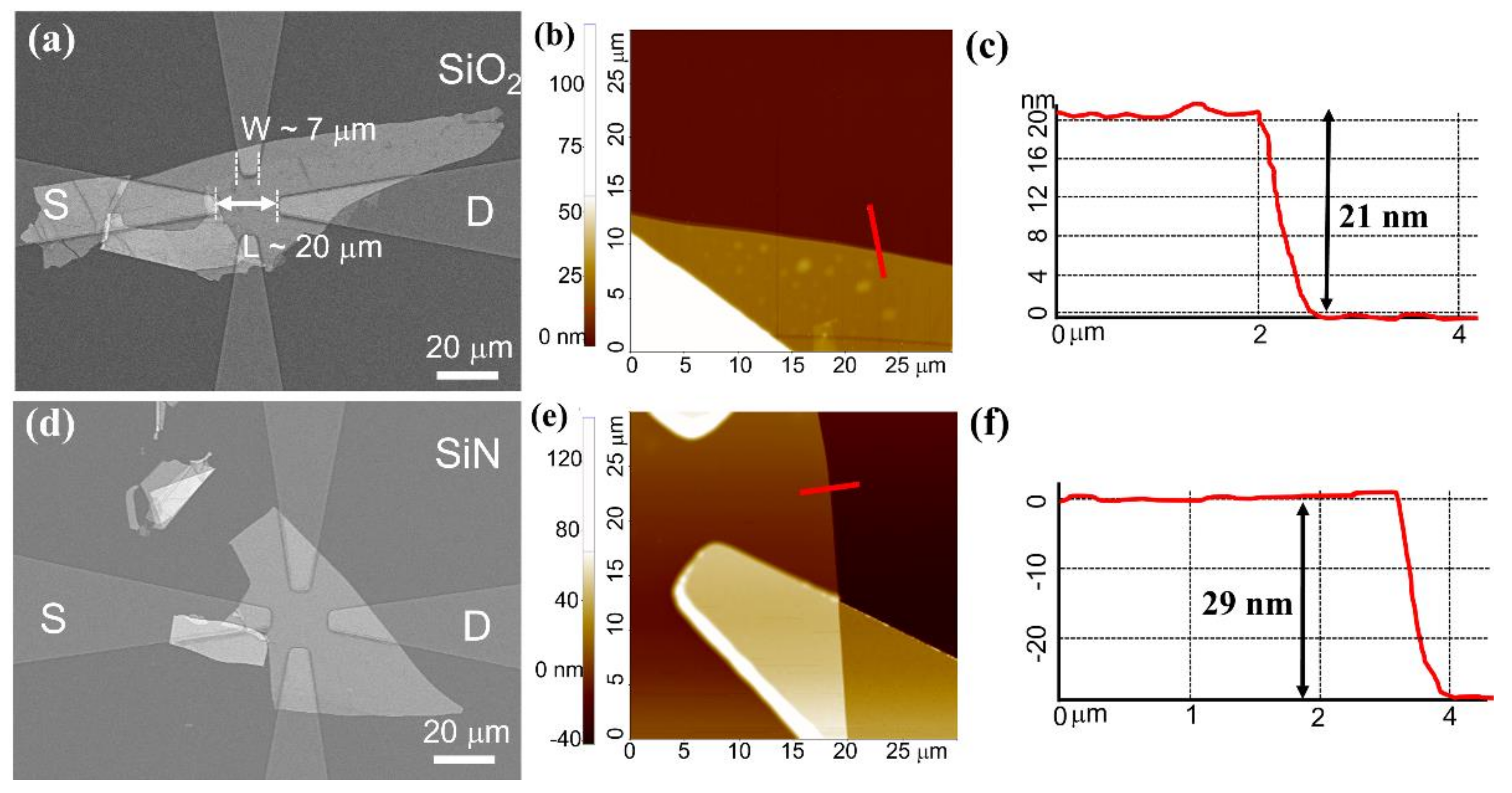
3.2. Morphological Characterization

Figure 2a,d show the SEM images of the devices (MoSe2/SiO2/Si with the MoSe2 thickness of 21 nm and MoSe2/SiN/Si with the MoSe2 thickness of 29 nm), the corresponding AFM images are shown in Figure 2b,e, and the topographic analysis for both devices are shown in Figure 2c,f. The channel length and width were 20 and 7 µm, respectively, as shown in Figure 2a.

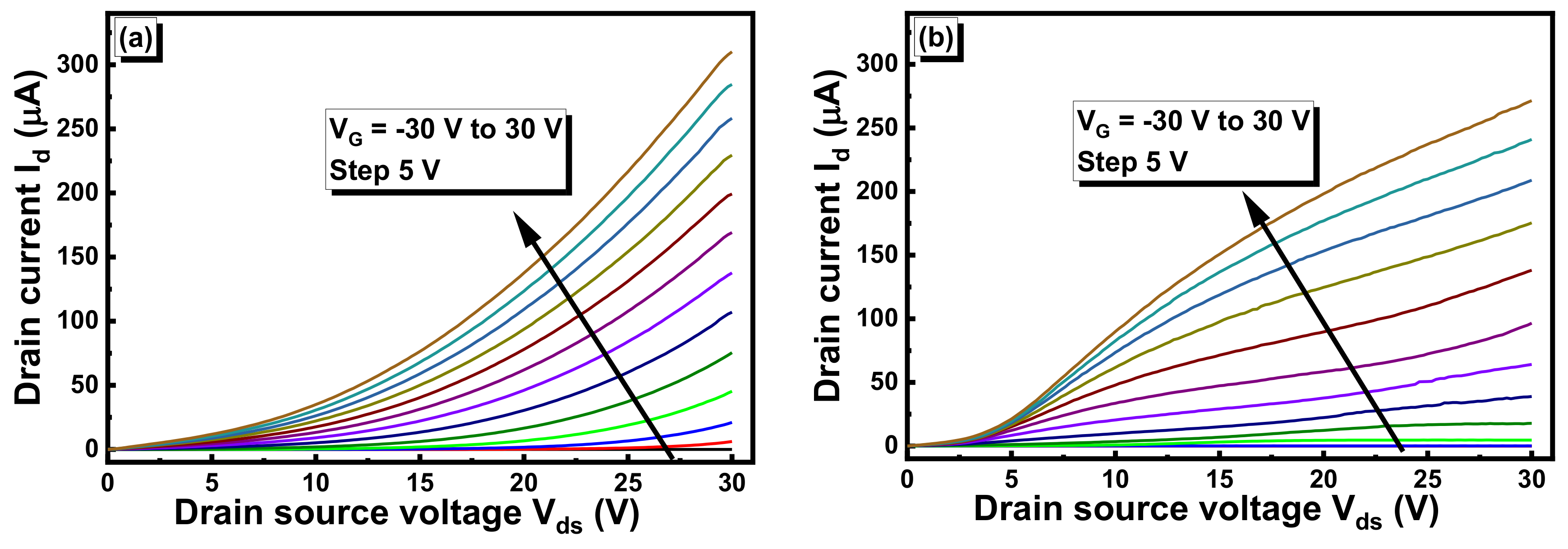
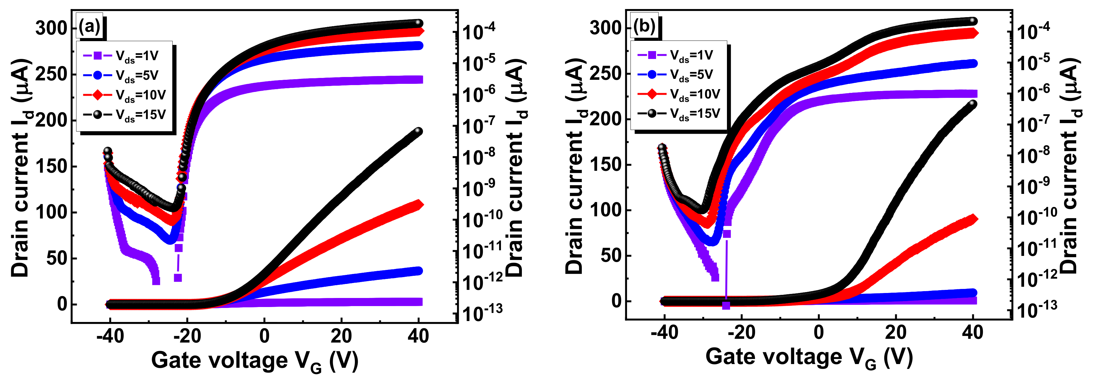
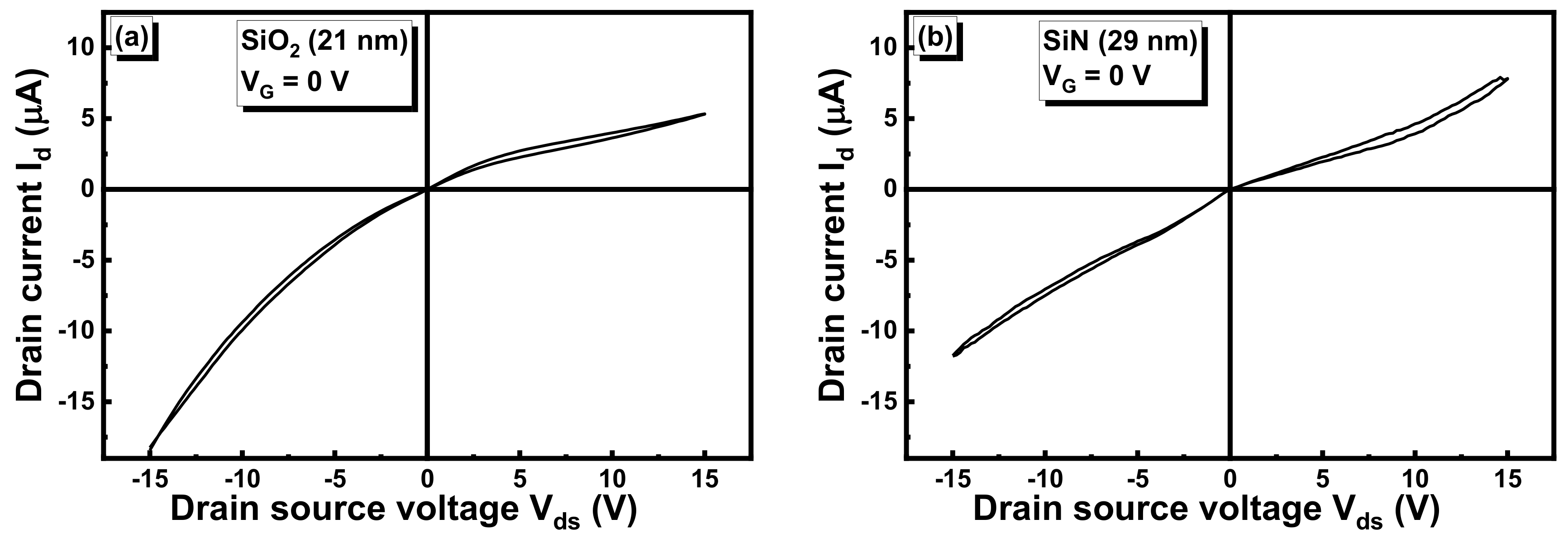
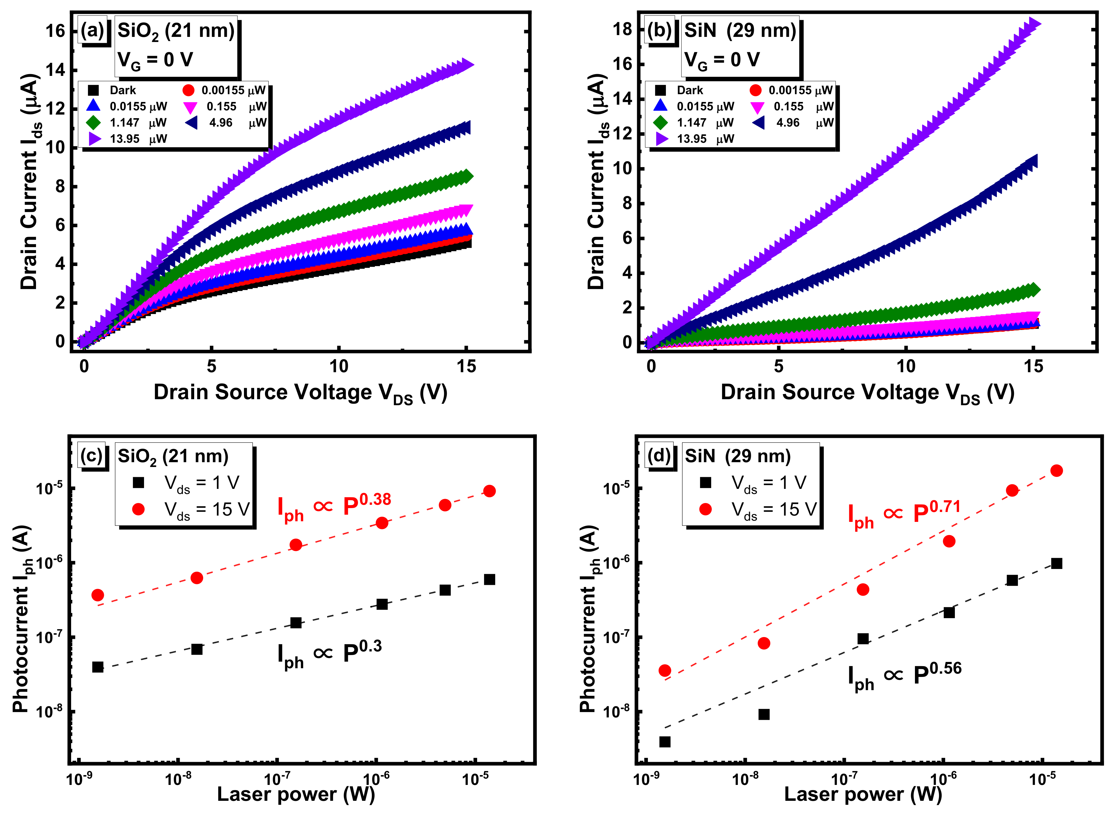
3.3. Electrical and Optoelectronic Characterization

The Id-Vds characteristics of both devices as a function of gate voltage are shown in Figure 3a,b. The MoSe2/SiO2/Si device exhibited Schottky-like behavior, while MoSe2/SiN/Si exhibited better and almost ohmic contact. Both devices showed good gate-voltage controllability of their current–voltage curves.

3.4. Electrical Characterizations of All Samples

Figure 4a,b show the variation in the transfer curves (Id–VG) versus the Vds. The current was measured by setting Vds to 1, 5, 10, or 15 V and varying the back-gate voltage from −40 V to 40 V. When VG increased to a positive value, the carrier density increased, and the current increased. Kink effects were observed in the MoSe2/SiN/Si device (Figure 4b) at the polarization voltages of 10 and 15 V. Similar behavior was observed in a previously reported MoSe2/h-BN/Si-based FET device [10] and FET devices based on 2D materials such as black phosphorus [13] and graphene [14]. The kink effect in our device can be explained by the effect of carrier de-trapping from the interface at a high polarization voltage during carrier transport. The Ion/Ioff values were 6.32 × 10², 3.49 × 10³, 8.04 × 10³, and 1.22 × 10⁴ at Vds values of 1, 5, 10, and 15 V, respectively, in the MoSe2/SiO2/Si device. However, in the MoSe2/SiN/Si device, the values were 5.92 × 101, 5.88 × 10², 5.27 × 10², and 1.27 × 10⁴ at 1, 5, 10, and 15 V, respectively.
The Id–Vds curves in both devices, in the absence of an applied VG, are shown in Figure 5. Very narrow hysteresis was observed in both devices, which originated from the trapping and de-trapping effects of charges at the interfaces and surface of MoSe2. It is well known that when multilayered MoSe2 is exposed to ambient air, oxygen molecules can be converted into chemisorbed oxygen anions (O2) on the surface of MoSe2, where they act as electron traps [15]. In addition to chemisorbed O2, humidity can induce trapping center formation [16]. Annealing devices in Ar can remove surface-adsorbed water vapor and oxygen [17]. However, charged impurities at the channel/SiO2 interface and charge traps in SiO2 can limit the electrical performance of FET [16,18]. Similar to SiO2, SiN can exhibit extrinsic charges owing to defect density and impurities, including hosting trapped charges and surface adsorbates [19].
Finally, we investigated the optoelectronic properties of the same devices under different laser excitation powers of 0.00155, 0.0155, 0.155, 1.147, 4.96, and 13.95 µW. Figure 6a,b show the Id–Vds characteristics at different laser powers of the MoSe2/SiO2/Si and MoSe2/SiN/Si devices, respectively. As expected, the current increased with increasing laser power. Thereafter, we deduced the photocurrent Iph according to the equation I ph = I ds i l l u m i n a t i o n I ds d a r k , then drew Iph as a function of the laser power (P) and interpolated the curve according to the equation I ph P α . Here, α can be used to determine the carrier transport origin [20,21], that is, if α is close to unity, the photoconductive effect dominates, and if α is close to zero, the photogating effect dominates. The photogating effect originates from the long-lived trap states [22,23]. As seen in Figure 6c,d, α is higher in the MoSe2/SiN/Si MISFET device, which means that the photoconductive effect is higher in this case. Photogating is dominant in the MoSe2/SiO2/Si MISFET (or MOSFET) device, which means that the trap concentration is higher in this case.

4. Conclusions

We fabricated eight MISFETs based on nanolayered MoSe2. We compared two devices with similar dimensions and different gate dielectric materials of SiO2 and SiN. The MoSe2/SiO2/Si- and MoSe2/SiN/Si-based MISFETs showed good electrical performance with high carrier mobility and high on/off ratios exceeding 104. Moreover, their current–voltage characteristics showed good gate-voltage controllability. In terms of carrier transport, the photoconductive effect is more apparent in the MoSe2/SiN/Si device, and the photogating effect is dominant in the MoSe2/SiO2/Si device; therefore, SiN can be a good alternative to SiO2, especially for optoelectronic devices such as high-speed photodetectors. In future research, the temperature dependence of the electrical properties of multilayered MoSe2-based MISFETs can be characterized with the aim of investigating the carrier trap density.

Author Contributions

Writing—review and editing, A.A. and P.-G.J.; formal analysis, C.W.; data curation, C.W.; writing—original draft preparation, P.J.K. All authors have read and agreed to the published version of the manuscript.

Funding

This work was supported by Brain Pool Program through the National Research Foundation of Korea (NRF) funded by the Ministry of Science and ICT (NRF-2019H1D3A1A01102658). This study was supported by research fund from Chosun University, 2022.

Conflicts of Interest

The authors declare no conflict of interest.

References

  1. Zheng, L.; Wang, X.; Jiang, H.; Xu, M.; Huang, W.; Liu, Z. Recent progress of flexible electronics by 2D transition metal dichalcogenides. Nano Res. 2022, 15, 2413–2432. [Google Scholar] [CrossRef]
  2. Zhao, L.; Shang, Q.; Li, M.; Liang, Y.; Li, C.; Zhang, Q. Strong exciton-photon interaction and lasing of two-dimensional transition metal dichalcogenide semiconductors. Nano Res. 2021, 14, 1937–1954. [Google Scholar] [CrossRef]
  3. Wang, L.; Xu, D.; Jiang, L.; Gao, J.; Tang, Z.; Xu, Y.; Chen, X.; Zhang, H. Transition metal dichalcogenides for sensing and oncotherapy: Status, challenges, and perspective. Adv. Funct. Mater. 2021, 31, 2004408. [Google Scholar] [CrossRef]
  4. Imani Yengejeh, S.; Wen, W.; Wang, Y. Mechanical properties of lateral transition metal dichalcogenide heterostructures. Front. Phys. 2021, 16, 13502. [Google Scholar] [CrossRef]
  5. Wu, M.; Xiao, Y.; Zeng, Y.; Zhou, Y.; Zeng, X.; Zhang, L.; Liao, W. Synthesis of two-dimensional transition metal dichalcogenides for electronics and optoelectronics. InfoMat 2021, 3, 362–396. [Google Scholar] [CrossRef]
  6. Saha, J.K.; Chakma, N.; Hasan, M. Impact of channel length, gate insulator thickness, gate insulator material, and temperature on the performance of nanoscale FETs. J. Comput. Electron. 2018, 17, 1521–1527. [Google Scholar] [CrossRef]
  7. Su, S.K.; Chuu, C.P.; Li, M.Y.; Cheng, C.C.; Wong, H.S.P.; Li, L.J. Layered semiconducting 2D materials for future transistor applications. Small Struct. 2021, 2, 2000103. [Google Scholar] [CrossRef]
  8. Cassabois, G.; Valvin, P.; Gil, B. Hexagonal boron nitride is an indirect bandgap semiconductor. Nat. Photonics 2016, 10, 262–266. [Google Scholar] [CrossRef]
  9. Sasama, Y.; Kageura, T.; Imura, M.; Watanabe, K.; Taniguchi, T.; Uchihashi, T.; Takahide, Y. High-mobility p-channel wide-bandgap transistors based on hydrogen-terminated diamond/hexagonal boron nitride heterostructures. Nat. Electron. 2022, 5, 37–44. [Google Scholar] [CrossRef]
  10. Abderrahmane, A.; Ko, P.J.; Jung, P.G.; Kim, N.H.; Sandhu, A. Optoelectronic characterizations of two-dimensional h-BN/MoSe2 heterostructures based photodetector. Sci. Adv. Mater. 2018, 10, 627–631. [Google Scholar] [CrossRef]
  11. Memaran, S. Lateral PN Junctions Based on 2-D Materials. Ph.D. Thesis, College of Arts and Sciences Florida State University, Tallahassee, FL, USA, 2018; pp. 18–24. [Google Scholar]
  12. Houssat, M.; Villeneuve-Faure, C.; Lahoud Dignat, N.; Locatelli, M.L.; Cambronne, J.P. Temperature Influence on PI/Si3N4 Nanocomposite Dielectric Properties: A Multiscale Approach. Polymers 2021, 13, 1936. [Google Scholar] [CrossRef]
  13. Xia, Y.; Li, G.; Jiang, B.; Yang, Z.; Liu, X.; Xiao, X.; Flandre, D.; Wang, C.; Liu, Y.; Liao, L. Exploring and suppressing the kink effect of black phosphorus field-effect transistors operating in the saturation regime. Nanoscale 2019, 11, 10420–10428. [Google Scholar] [CrossRef]
  14. Meric, I.; Han, M.Y.; Young, A.F.; Ozyilmaz, B.; Kim, P.; Shepard, K.L. Current saturation in zero-bandgap, top-gated graphene field-effect transistors. Nat. Nanotechnol. 2008, 3, 654–659. [Google Scholar] [CrossRef]
  15. Zhang, D.; Yang, Z.; Li, P.; Pang, M.; Xue, Q. Flexible self-powered high-performance ammonia sensor based on Au-decorated MoSe2 nanoflowers driven by single layer MoS2-flake piezoelectric nanogenerator. Nano Energy 2019, 65, 103974. [Google Scholar] [CrossRef]
  16. Lee, H.; Kim, J.H.; Lee, C.J. Electrical characteristics of MoSe2 TFTs dependent on the Al2O3 capping layer. Appl. Phys. Lett. 2016, 109, 222105. [Google Scholar] [CrossRef]
  17. Guo, S.; Yang, D.; Zhang, S.; Dong, Q.; Li, B.; Tran, N.; Li, Z.; Xiong, Y.; Zaghloul, M.E. Development of a cloud-based epidermal MoSe2 device for hazardous gas sensing. Adv. Funct. Mater. 2019, 29, 1900138. [Google Scholar] [CrossRef]
  18. Chamlagain, B.; Li, Q.; Ghimire, N.J.; Chuang, H.J.; Perera, M.M.; Tu, H.; Xu, Y.; Pan, M.; Xaio, D.; Yan, J.; et al. Mobility improvement and temperature dependence in MoSe2 field-effect transistors on parylene-C substrate. ACS Nano 2014, 8, 5079–5088. [Google Scholar] [CrossRef]
  19. Shao, F.; Woo, S.Y.; Wu, N.; Schneider, R.; Mayne, A.J.; de Vasconcellos, S.M.; Arora, A.; Carey, B.J.; Preuß, J.A.; Bonnet, N.; et al. Substrate influence on transition metal dichalcogenide monolayer exciton absorption linewidth broadening. Phys. Rev. Mater. 2022, 6, 074005. [Google Scholar] [CrossRef]
  20. Fang, H.; Hu, W. Photogating in low dimensional photodetectors. Adv. Sci. 2017, 4, 1700323. [Google Scholar] [CrossRef]
  21. Huang, H.; Wang, J.; Hu, W.; Liao, L.; Wang, P.; Wang, X.; Gong, F.; Chen, Y.; Wu, G.; Luo, W.; et al. Highly sensitive visible to infrared MoTe2 photodetectors enhanced by the photogating effect. Nanotechnology 2016, 27, 445201. [Google Scholar] [CrossRef]
  22. Fu, S.; du Fossé, I.; Jia, X.; Xu, J.; Yu, X.; Zhang, H.; Zheng, W.; Krasel, S.; Chen, Z.; Wang, Z.M.; et al. Long-lived charge separation following pump-wavelength–dependent ultrafast charge transfer in graphene/WS2 heterostructures. Sci. Adv. 2021, 7, eabd9061. [Google Scholar] [CrossRef]
  23. Island, J.O.; Blanter, S.I.; Buscema, M.; van der Zant, H.S.; Castellanos-Gomez, A. Gate controlled photocurrent generation mechanisms in high-gain In2Se3 phototransistors. Nano Lett. 2015, 15, 7853–7858. [Google Scholar] [CrossRef] [Green Version]
Figure 1. Id-Vds characteristics of the fabricated devices on (a) SiO2/Si substrates and (b) SiN/Si substrates, and transfer curves of the fabricated devices on (c) SiO2/Si substrates and (d) SiN/Si substrates.
Crystals 12 01301 g001aCrystals 12 01301 g001b
Figure 2. (a) SEM image of MoSe2/SiO2/Si (magnification 1k); (b,c) the corresponding AFM image and topographic analysis, respectively. (d) SEM image of MoSe2/SiN/Si (magnification 1k); (e,f) the corresponding AFM image and topographic analysis, respectively.
Crystals 12 01301 g002
Figure 3. Id-Vds characteristics of the fabricated devices on (a) SiO2/Si substrates and (b) SiN/Si substrates, at different gate voltages.
Crystals 12 01301 g003
Figure 4. Transfer curves (Id-VG) at various Vds values for MISFET devices of (a) MoSe2/SiO2/Si and (b) MoSe2/SiN/Si.
Crystals 12 01301 g004
Figure 5. Id-Vds sweeps of (a) MoSe2/SiO2/Si and (b) MoSe2/SiN/Si MISFET devices.
Crystals 12 01301 g005
Figure 6. Id-Vds characteristics of the fabricated devices on (a) SiO2/Si substrates and (b) SiN/Si substrates, at different laser powers. (c,d) The photocurrent Iph as a function of the laser power at two polarization voltages.
Crystals 12 01301 g006
Table 1. Electrical mobilities, subthreshold swing (ss) values, and on/off ratios of MISFETs.
PropertySiO2SiO2SiO2SiO2SiNSiNSiNSiN
7 nm21 nm63 nm90 nm29 nm36 nm47 nm87 nm
μ eff (cm2/V·s)0.872.0116.543.563.955.551.3164.0
ss (mV/dec)3.7 × 1031.4 × 1035.0 × 1032.8 × 1042.6 × 1032.5 × 1031.5 × 1033.7 × 103
On/Off ratio7.0 × 1021.2 × 1041.0 × 1043.1 × 1011.2 × 1049 × 1031.7 × 1059.6 × 102
Publisher’s Note: MDPI stays neutral with regard to jurisdictional claims in published maps and institutional affiliations.

