
Performance Analysis of DAST Material-Assisted Photonic-Crystal-Based Electrical Tunable Optical Filter


Abstract
:1. Introduction
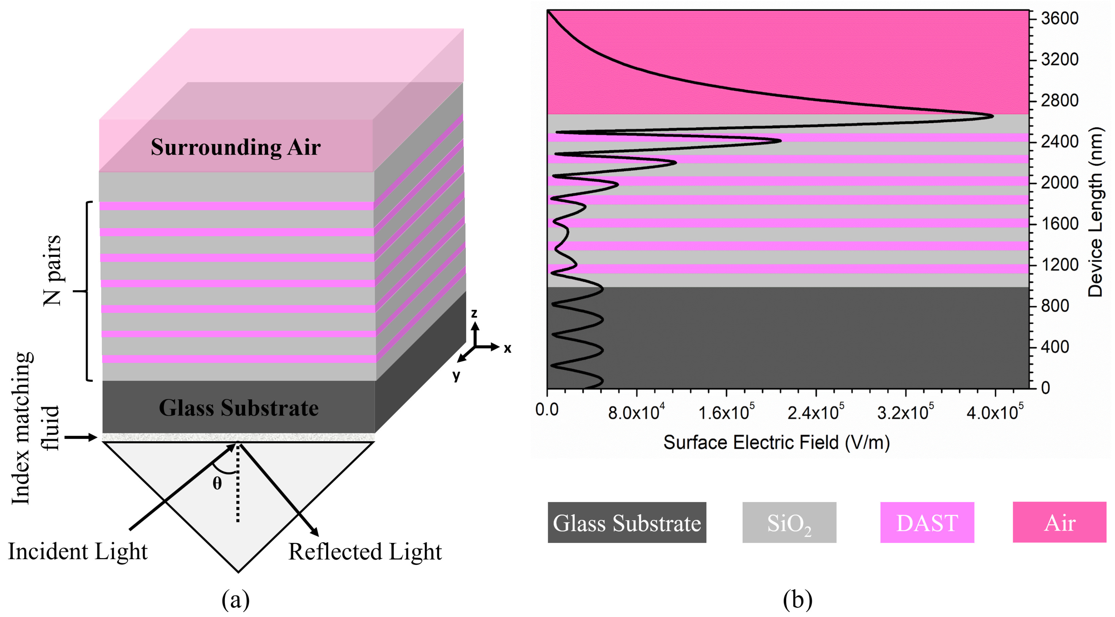
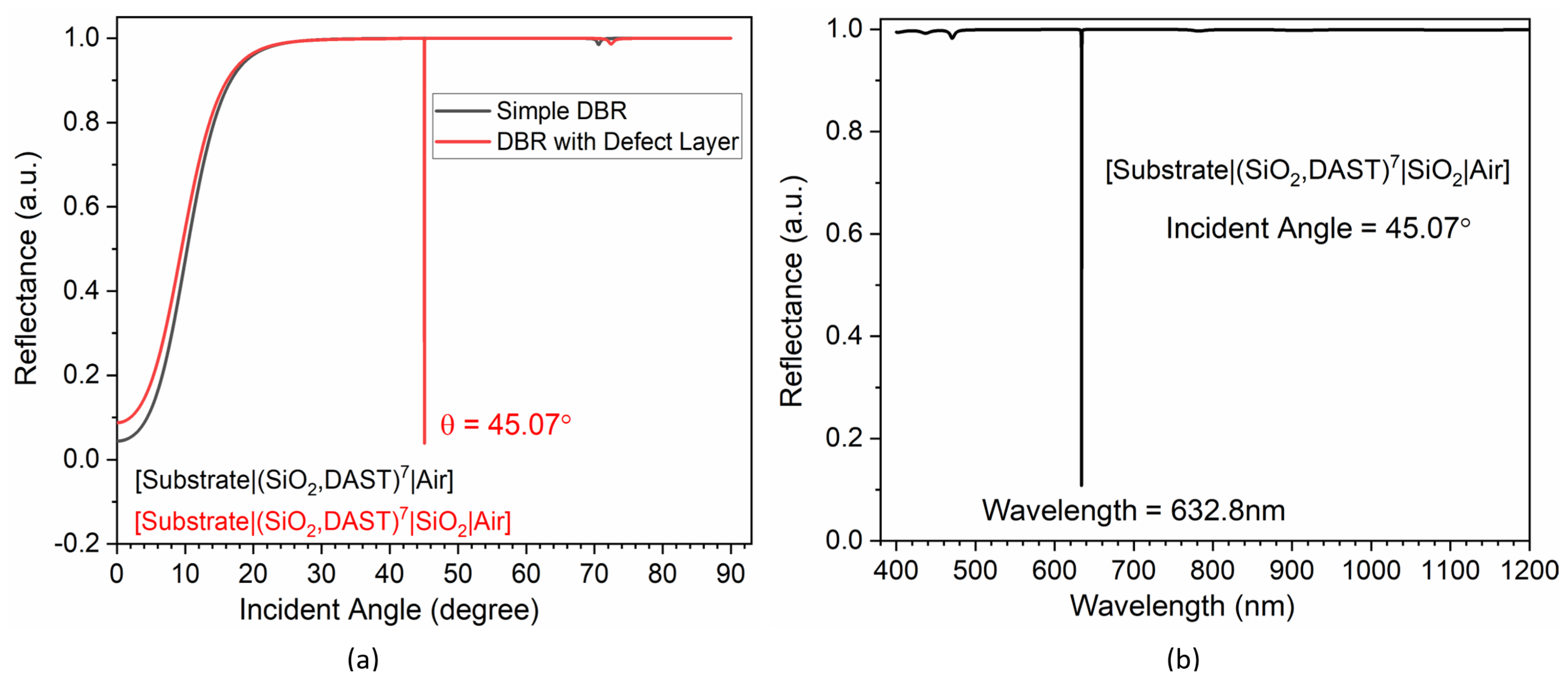
2. Design Methodology and Optimization
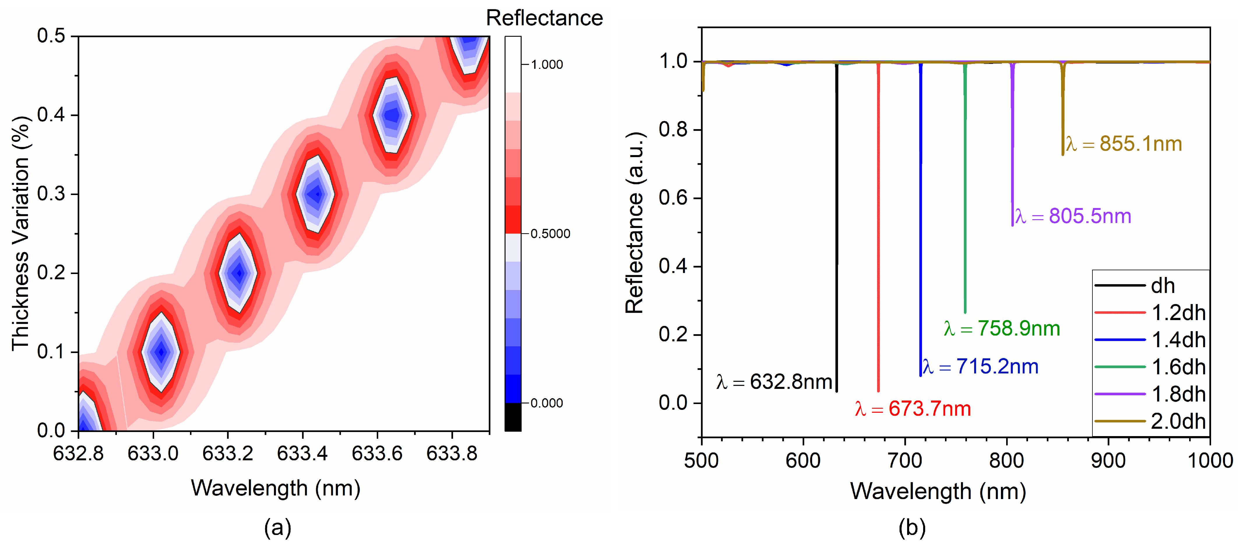
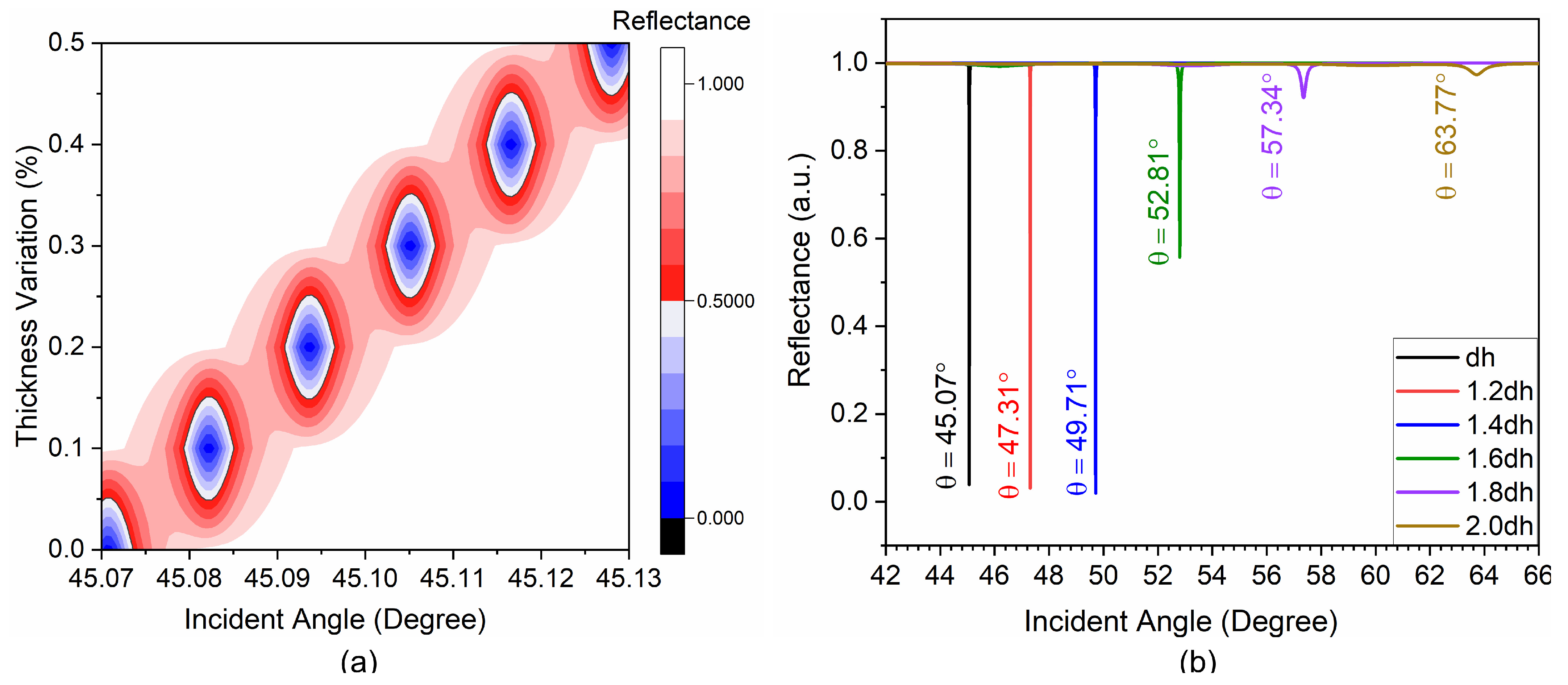
3. Simulation Results and Discussion
4. Conclusions
Author Contributions
Funding
Institutional Review Board Statement
Informed Consent Statement
Data Availability Statement
Conflicts of Interest
References
- Neubrech, F.; Duan, X.; Liu, N. Dynamic plasmonic color generation enabled by functional materials. Sci. Adv. 2020, 6, eabc2709. [Google Scholar] [CrossRef] [PubMed]
- Duan, X.; Liu, N. Magnesium for dynamic nanoplasmonics. Acc. Chem. Res. 2019, 52, 1979–1989. [Google Scholar] [CrossRef] [PubMed] [Green Version]
- Sharma, M.; Hendler, N.; Ellenbogen, T. Electrically switchable color tags based on active liquid-crystal plasmonic metasurface platform. Adv. Opt. Mater. 2020, 8, 1901182. [Google Scholar] [CrossRef]
- Shahabuddin, M.; McDowell, T.; Bonner, C.E.; Noginova, N. Enhancement of electrochromic polymer switching in plasmonic nanostructured environment. ACS Appl. Nano Mater. 2019, 2, 1713–1719. [Google Scholar] [CrossRef]
- Aly, A.H.; Sayed, F.A.; Hussein, A.E. Defect mode tunability based on the electro-optical characteristics of the one-dimensional graphene photonic crystals. Appl. Opt. 2020, 59, 4796–4805. [Google Scholar] [CrossRef]
- Wuttig, M.; Bhaskaran, H.; Taubner, T. Phase-change materials for non-volatile photonic applications. Nat. Photonics 2017, 11, 465. [Google Scholar] [CrossRef]
- Jeong, H.D.; Lee, S.Y. Tunable plasmonic absorber using a nano slit array patterned on a Ge2Sb2Te5-inserted Fabry–Perot resonator. J. Light. Technol. 2018, 36, 5857–5862. [Google Scholar] [CrossRef]
- Zhao, Z. Sn dopants improve the visible transmittance of VO2 films achieving excellent thermos-chromic performance for smart window. Sol. Energy Mater. Sol. Cells 2020, 209, 110443. [Google Scholar] [CrossRef]
- Alam, M.; Massoud, Y. RLC ladder model for scattering in single metallic nanoparticles. IEEE Trans. Nanotechnol. 2006, 5, 491–498. [Google Scholar] [CrossRef]
- Goyal, A.K.; Saini, J. Performance Analysis of Bloch Surface Wave Based Sensor using Transition Metal Dichalcogenides. Appl. Nanosci. 2020, 10, 4307–4313. [Google Scholar] [CrossRef]
- Meade, R.D.; Brommer, K.D.; Rappe, A.M.; Joannopoulos, J.D. Electromagnetic Bloch waves at the surface of a photonic crystal. Phys. Rev. B 1991, 44, 10961. [Google Scholar] [CrossRef] [PubMed]
- Dutta, H.S.; Goyal, A.K.; Pal, S. Analysis of Dispersion Diagram for High Performance Refractive Index Sensor based on Photonic Crystal Waveguides. Photonics Nanostruct. 2017, 23, 21–27. [Google Scholar] [CrossRef]
- Robertson, W.M.; Arjavalingam, G.; Meade, R.D.; Brommer, K.D.; Rappe, A.M.; Joannopoulos, J.D. Observation of surface photons on periodic dielectric arrays. Opt. Lett. 1993, 18, 528–530. [Google Scholar] [CrossRef] [PubMed] [Green Version]
- Goyal, A.K.; Kumar, A.; Massoud, Y. Thermal Stability Analysis of Surface Wave Assisted Bio-Photonic Sensor. Photonics 2022, 9, 324. [Google Scholar] [CrossRef]
- Duan, X.; Kamin, S.; Liu, N. Dynamic plasmonic colour display. Nat. Commun. 2017, 8, 14606. [Google Scholar] [CrossRef] [Green Version]
- Xiong, K.; Tordera, D.; Jonsson, M.P.; Dahlin, A.B. Active control of plasmonic colors: Emerging display technologies. Rep. Prog. Phys. 2019, 82, 024501. [Google Scholar] [CrossRef] [Green Version]
- Damgaard-Carstensen, C.; Thomaschewski, M.; Ding, F.; Bozhevolnyi, S.I. Electrical Tuning of Fresnel Lens in Reflection. ACS Photonics 2021, 8, 1576–1581. [Google Scholar] [CrossRef]
- Gat, N. Imaging spectroscopy using tunable filters: A review. Proc. SPIE 2000, 4056, 50–64. [Google Scholar]
- Ebermann, M.; Neumann, N.; Hiller, K.; Seifert, M.; Meinig, M.; Kurth, S. Tunable MEMS Fabry-Pérot filters for infrared micro spectrometers: A review. Proc. SPIE 2016, 9760, 97600H1-20. [Google Scholar]
- Gebhart, S.C.; Thompson, R.C.; Mahadevan-Jansen, A. Liquid crystal tunable filter spectral imaging for brain tumor demarcation. Appl. Opt. 2007, 46, 1896–1910. [Google Scholar] [CrossRef]
- Hosseini, A.; Massoud, Y. Optical range microcavities and filters using multiple dielectric layers in metal-insulator-metal structures. J. Opt. Soc. Am. A 2007, 24, 221–224. [Google Scholar] [CrossRef] [PubMed]
- Ratra, K.; Singh, M.; Goyal, A.K. Design and Analysis of Omni-directional Solar Spectrum Reflector using One-dimensional Photonic Crystal. J. Nanophotonics 2020, 14, 026005. [Google Scholar] [CrossRef]
- Hosseini, A.; Nejati, H.; Massoud, Y. Design of a maximally flat optical low pass filter using plasmonic nanostrip waveguides. Opt. Express 2007, 15, 15280–15286. [Google Scholar] [CrossRef] [PubMed]
- Chen, Q.; Gao, F.; Wang, D.N.; Wang, Z.; Wang, Y. Electrically tunable optical filter based on tapered fiber coated with porous graphene film. Opt. Commun. 2022, 505, 127518. [Google Scholar] [CrossRef]
- Heenkenda, R.; Hirakawa, K.; Sarangan, A. Tunable optical filter using phase change materials for smart IR night vision applications. Opt. Express 2021, 29, 33795–33803. [Google Scholar] [CrossRef]
- Mirshafieyan, S.S.; Gregory, D.A. Electrically tunable perfect light absorbers as color filters and modulators. Sci. Rep. 2018, 8, 2635. [Google Scholar] [CrossRef] [Green Version]
- Ahmed, U.; Khan, Y.; Ehsan, M.K.; Amirzada, M.R.; Ullah, N.; Khatri, A.R.; Ur Rehman, A.; Butt, M.A. Investigation of Spectral Properties of DBR-Based Photonic Crystal Structure for Optical Filter Application. Crystals 2022, 12, 409. [Google Scholar] [CrossRef]
- Khan, Y.; Rehman, A.U.; Batool, B.A.; Noor, M.; Butt, M.A.; Kazanskiy, N.L.; Khonina, S.N. Fabrication and Investigation of Spectral Properties of a Dielectric Slab Waveguide Photonic Crystal Based Fano-Filter. Crystals 2022, 12, 226. [Google Scholar] [CrossRef]
- Marder, S.R.; Perry, J.W.; Schaefer, W.P. Synthesis of organic salts with large 2nd-order optical nonlinearities. Science 1989, 245, 626–628. [Google Scholar] [CrossRef]
- Vicario, C.; Jazbinsek, M.; Ovchinnikov, A.V.; Chefonov, O.V.; Ashitkov, S.I.; Agranat, M.B.; Hauri, C.P. High efficiency THz generation in DSTMS, DAST and OH1 pumped by Cr: Forsterite laser. Opt. Express 2015, 23, 4573–4580. [Google Scholar] [CrossRef] [Green Version]
- Stepanov, A.G.; Bonacina, L.; Wolf, J. DAST/SiO2 multilayer structure for efficient generation of 6 THz quasi-single-cycle electromagnetic pulses. Opt. Lett. 2012, 37, 2439–2441. [Google Scholar] [CrossRef] [PubMed]
- Chowdhary, A.; Sikdar, D. Design of electrotunable all-weather smart windows. Sol. Energy Mater. Sol. Cells 2021, 222, 110921. [Google Scholar] [CrossRef]
- Aalizadeh, M.; Serebryannikov, A.E.; Khavasi, A.; Vandenbosch, G.; Ozbay, E. Toward Electrically Tunable, Lithography-Free, Ultra-Thin Color Filters Covering the Whole Visible Spectrum. Sci. Rep. 2018, 8, 11316. [Google Scholar] [CrossRef] [PubMed]
- Jazbinsek, M.; Mutter, L.; Gunter, P. Photonic applications with the organic nonlinear optical crystal DAST. IEEE J. Sel. Top. Quantum Electron. 2008, 14, 1298–1311. [Google Scholar] [CrossRef]
- Robertson, W.M. Experimental Measurement of the Effect of Termination on Surface Electromagnetic Waves in One-Dimensional Photonic Bandgap Arrays. J. Light. Technol. 1999, 17, 2013. [Google Scholar] [CrossRef]
- Li, Y. Phase properties of Bloch surface waves and their sensing applications. Appl. Phys. Lett. 2013, 103, 041116. [Google Scholar] [CrossRef]
- Wang, Z.; Zhou, P.; Zheng, G. Electrically switchable highly efficient epsilon-near zero metasurfaces absorber with broadband response. Results Phys. 2019, 14, 102376. [Google Scholar] [CrossRef]
- Pochi, Y. Electromagnetic propagation in periodic stratified media I. General theory. J. Opt. Soc. Am. 1977, 67, 423–438. [Google Scholar]
- Hosseini, A.; Nejati, H.; Massoud, Y. Triangular lattice plasmonic photonic band gaps in subwavelength metal-insulator-metal waveguide structures. Appl. Phys. Lett. 2008, 92, 013116. [Google Scholar] [CrossRef]
- Goyal, A.K. Design Analysis of One-dimensional Photonic Crystal Based Structure for Hemoglobin Concentration Measurement. Prog. Electromagn. Res. M 2020, 97, 77–86. [Google Scholar] [CrossRef]
- Goyal, A.K.; Dutta, H.S.; Pal, S. Porous photonic crystal structure for sensing applications. J. Nanophotonics 2018, 12, 040501. [Google Scholar] [CrossRef]
- Hosseini, A.; Nieuwoudt, A.; Massoud, Y. Efficient simulation of subwavelength plasmonic waveguides using implicitly restarted Arnoldi. Opt. Exp. 2006, 14, 7291–7298. [Google Scholar] [CrossRef] [PubMed]
- Zhu, Y.J.; Huang, X.G.; Mei, X. A Surface Plasmon Polariton Electro-Optic Switch Based on a Metal-Insulator-Metal Structure with a Strip Waveguide and Two Side-Coupled Cavities. Chin. Phys. Lett. 2012, 29, 064214. [Google Scholar] [CrossRef]
- Taheri, A.N.; Kaatuzian, H. Numerical investigation of a nano-scale electro-plasmonic switch based on metal-insulator-metal stub filter. Opt. Quant. Electron. 2015, 47, 159–168. [Google Scholar] [CrossRef]
- Guo, J.J. Electrically Tunable Gap Surface Plasmon-based Metasurface for Visible Light. Sci. Rep. 2017, 7, 14078. [Google Scholar] [CrossRef] [Green Version]
- Goyal, A.K.; Kumar, A. Recent advances and progresses in photonic devices for passive radiative cooling application: A review. J. Nanophotonics 2020, 14, 030901. [Google Scholar] [CrossRef]
- Goyal, A.K.; Dutta, H.S.; Singh, S.; Kaur, M.; Husale, S.; Pal, S. Realization of Large-Scale Photonic Crystal Cavity-Based Devices. J. Micro/Nanolith. Mems Moems 2016, 15, 031608. [Google Scholar] [CrossRef]
- Goyal, A.K.; Dutta, H.S.; Pal, S. Development of Uniform Porous One-dimensional Photonic Crystal Based Sensor. Optik 2020, 223, 165597. [Google Scholar] [CrossRef]


| Thickness Variation | Incident Angle at Fixed Wavelength of 632.8 nm | Filtered Wavelength at Fixed Angle of 45.07 |
|---|---|---|
| 1.0 × dh | 45.07 C | 632.80 nm |
| 1.2 × dh | 47.31 C | 673.73 nm |
| 1.4 × dh | 49.71 C | 715.29 nm |
| 1.6 × dh | 52.81 C | 758.97 nm |
| 1.8 × dh | 57.34 C | 805.53 nm |
| 2.0 × dh | 63.77 C | 855.12 nm |
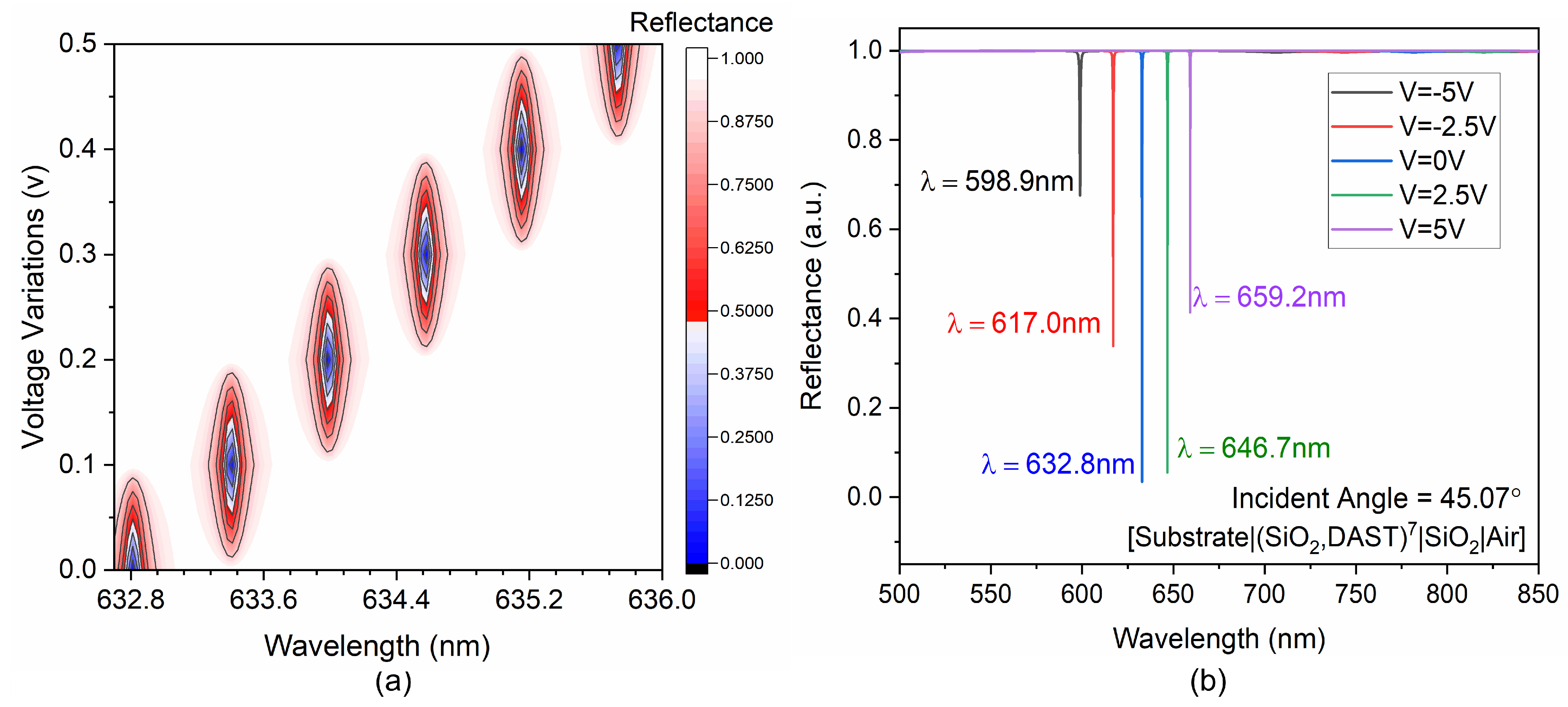
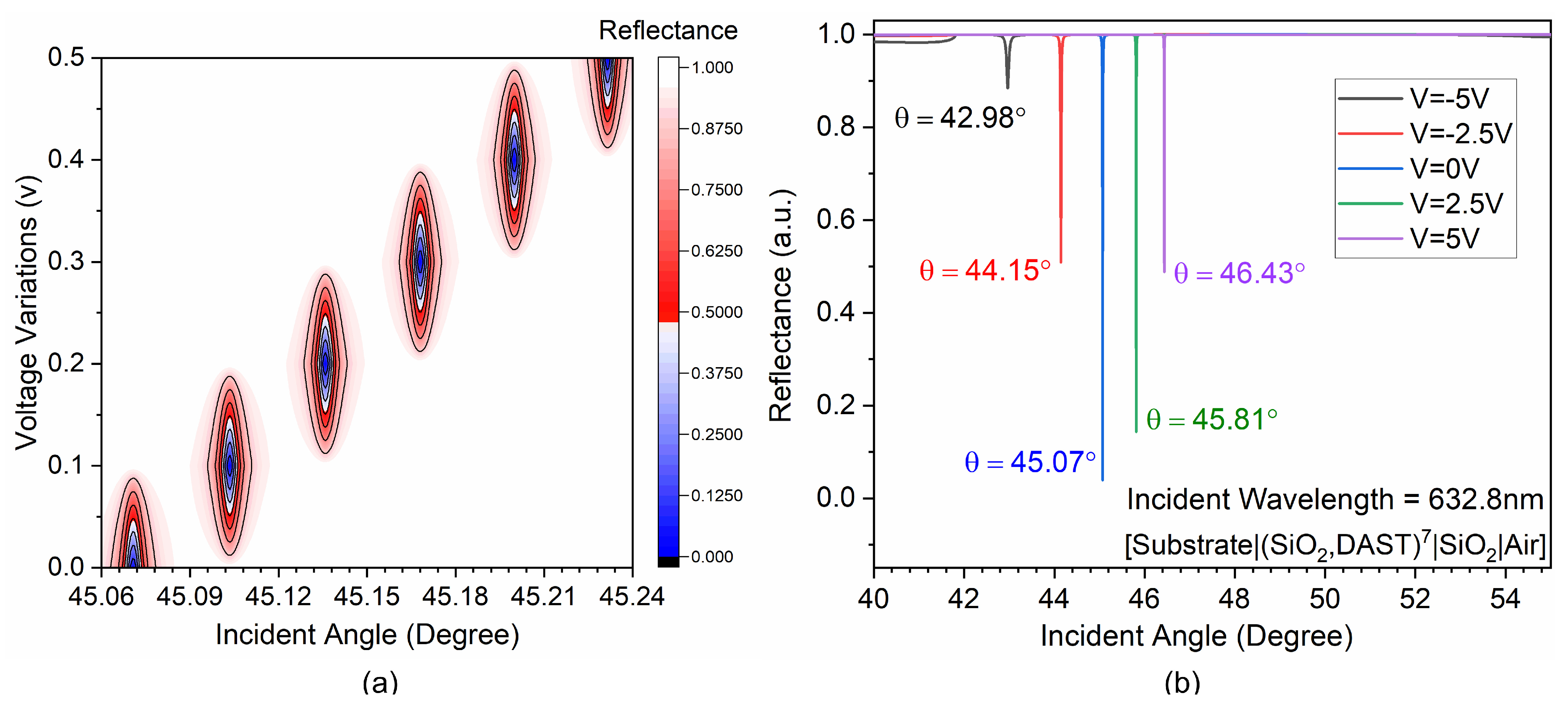
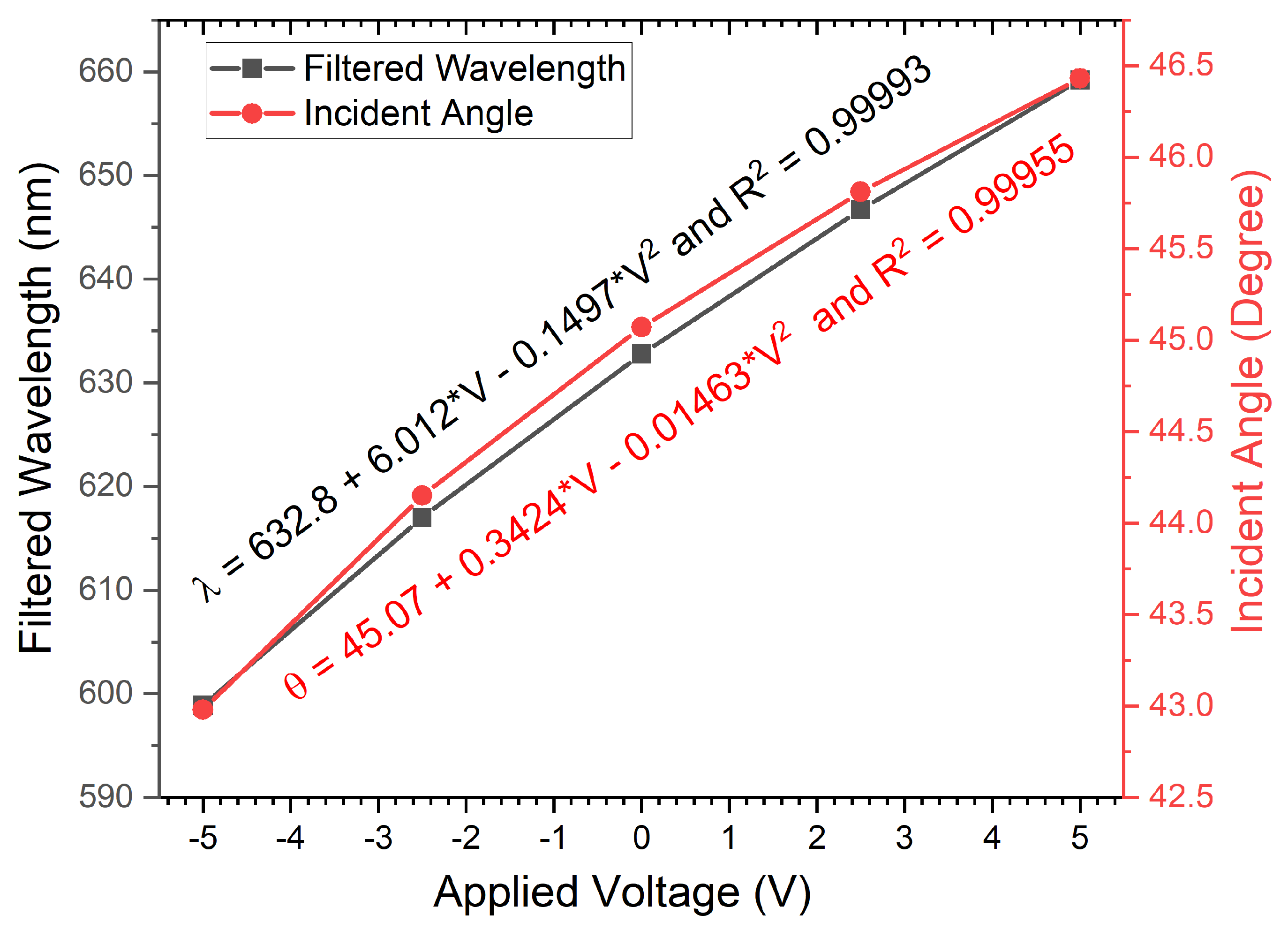
| Bias Voltage | Angular Interrogation | Wavelength Interrogation | ||
|---|---|---|---|---|
| Incidence Angle | FWHM | Resonance Wavelength | FWHM | |
| −5.0 | 42.98 C | 0.06 C | 598.9 nm | 0.45 nm |
| −2.5 | 44.15 C | 0.007 C | 617.0 nm | 0.18 nm |
| 0 | 45.07 C | 0.006 C | 632.8 nm | 0.11 nm |
| 2.5 | 45.81 C | 0.004 C | 646.7 nm | 0.07 nm |
| 5.0 | 46.43 C | 0.005 C | 659.2 nm | 0.08 nm |
Publisher’s Note: MDPI stays neutral with regard to jurisdictional claims in published maps and institutional affiliations. |
© 2022 by the authors. Licensee MDPI, Basel, Switzerland. This article is an open access article distributed under the terms and conditions of the Creative Commons Attribution (CC BY) license (https://creativecommons.org/licenses/by/4.0/).
Share and Cite
Goyal, A.K.; Kumar, A.; Massoud, Y. Performance Analysis of DAST Material-Assisted Photonic-Crystal-Based Electrical Tunable Optical Filter. Crystals 2022, 12, 992. https://doi.org/10.3390/cryst12070992
Goyal AK, Kumar A, Massoud Y. Performance Analysis of DAST Material-Assisted Photonic-Crystal-Based Electrical Tunable Optical Filter. Crystals. 2022; 12(7):992. https://doi.org/10.3390/cryst12070992
Chicago/Turabian StyleGoyal, Amit Kumar, Ajay Kumar, and Yehia Massoud. 2022. "Performance Analysis of DAST Material-Assisted Photonic-Crystal-Based Electrical Tunable Optical Filter" Crystals 12, no. 7: 992. https://doi.org/10.3390/cryst12070992