
Progress of Photonic-Crystal Surface-Emitting Lasers: A Paradigm Shift in LiDAR Application
 , , ,
, , , 
Abstract
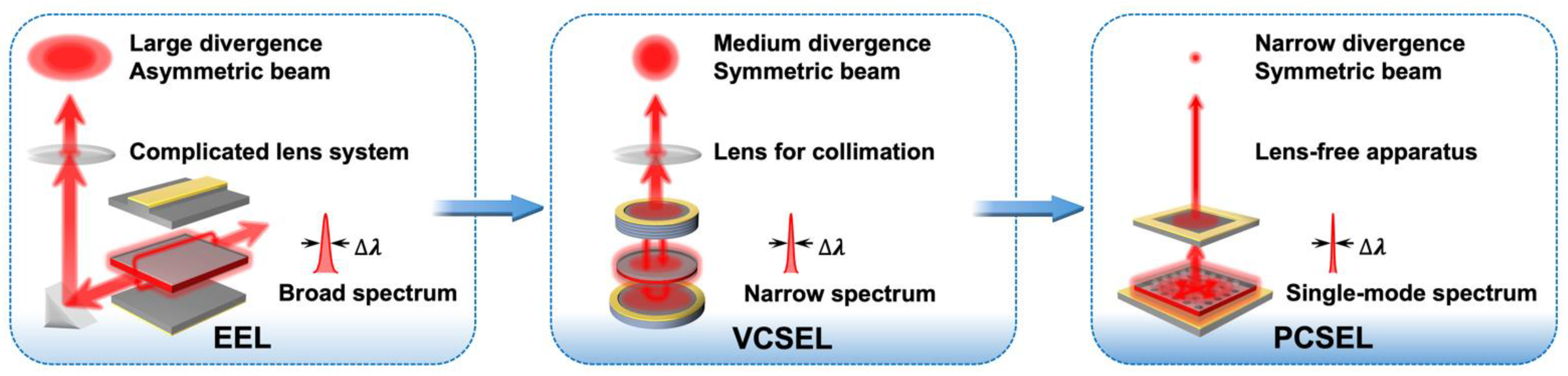
:1. Introduction
2. Analysis of PCSEL Technology Fronts
2.1. Methodology
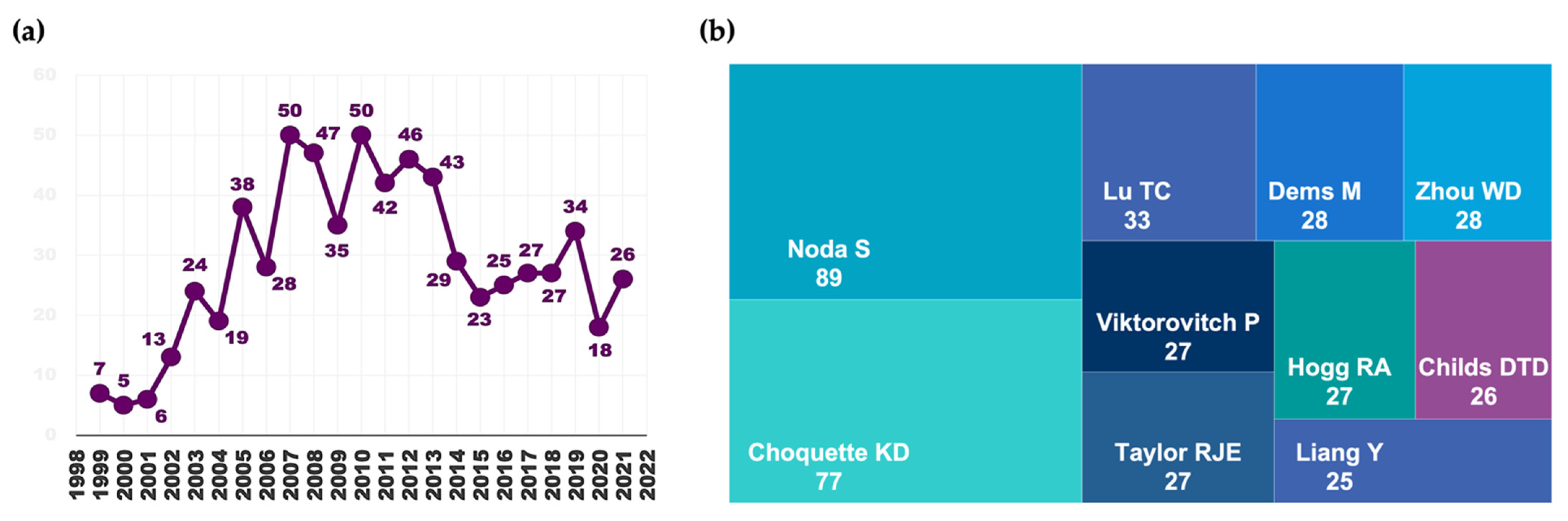
2.2. Overview of Relevant Publications from Web of Science (WoS)
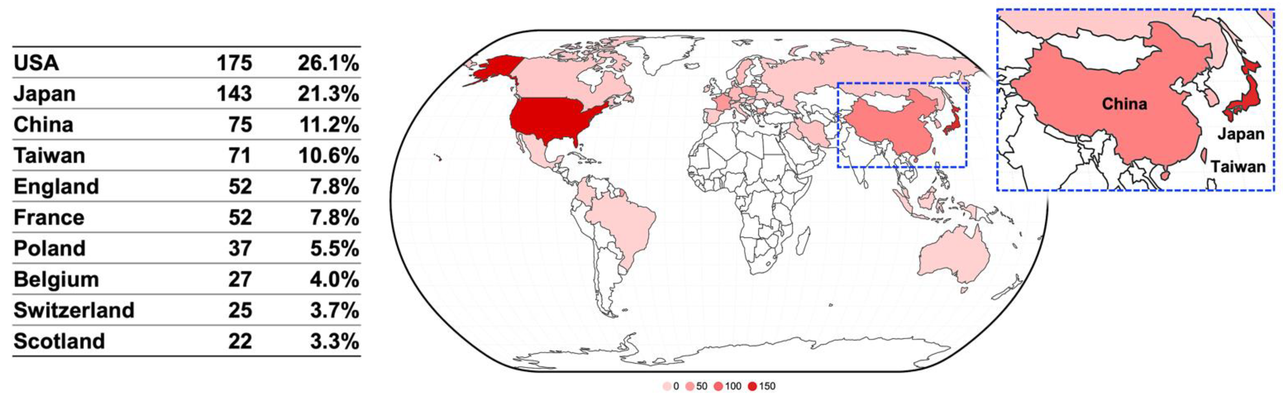
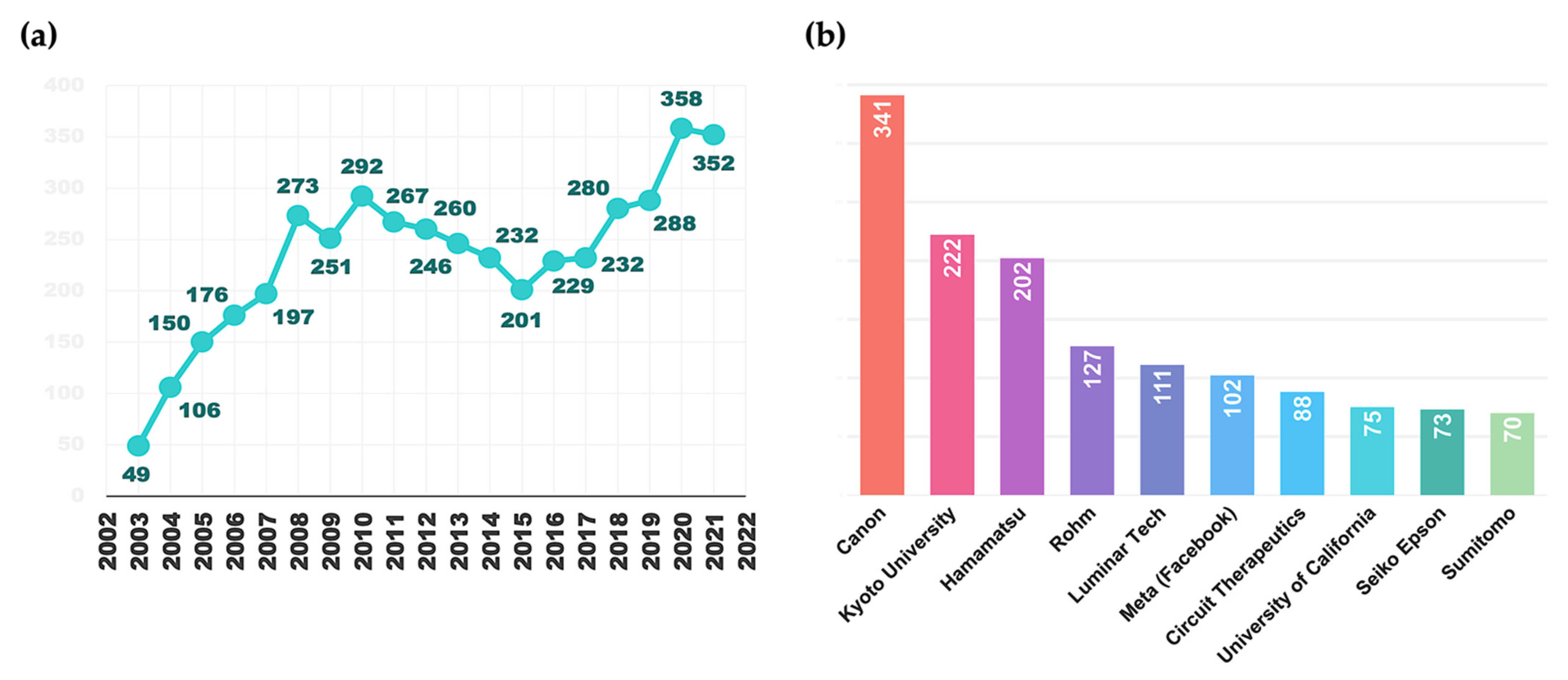
2.3. Overview of Relevant Patents around the World
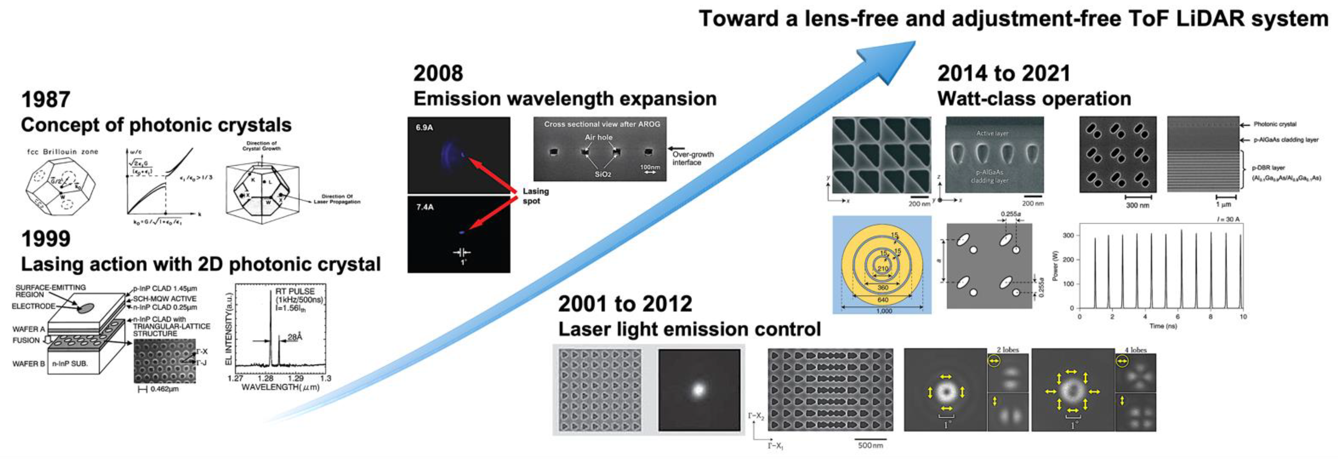
3. Progress in PCSEL Technology
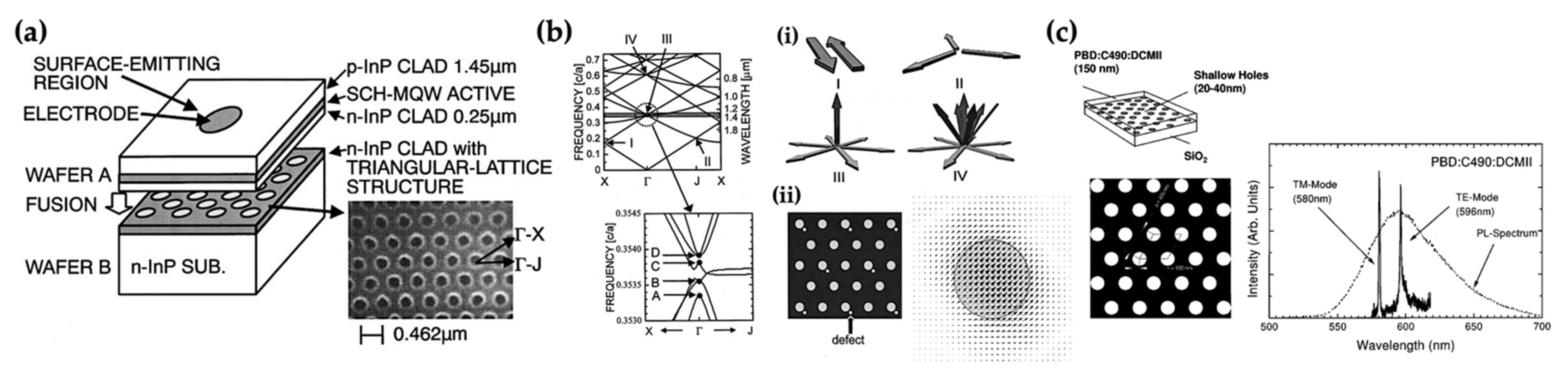
3.1. Operation Principle
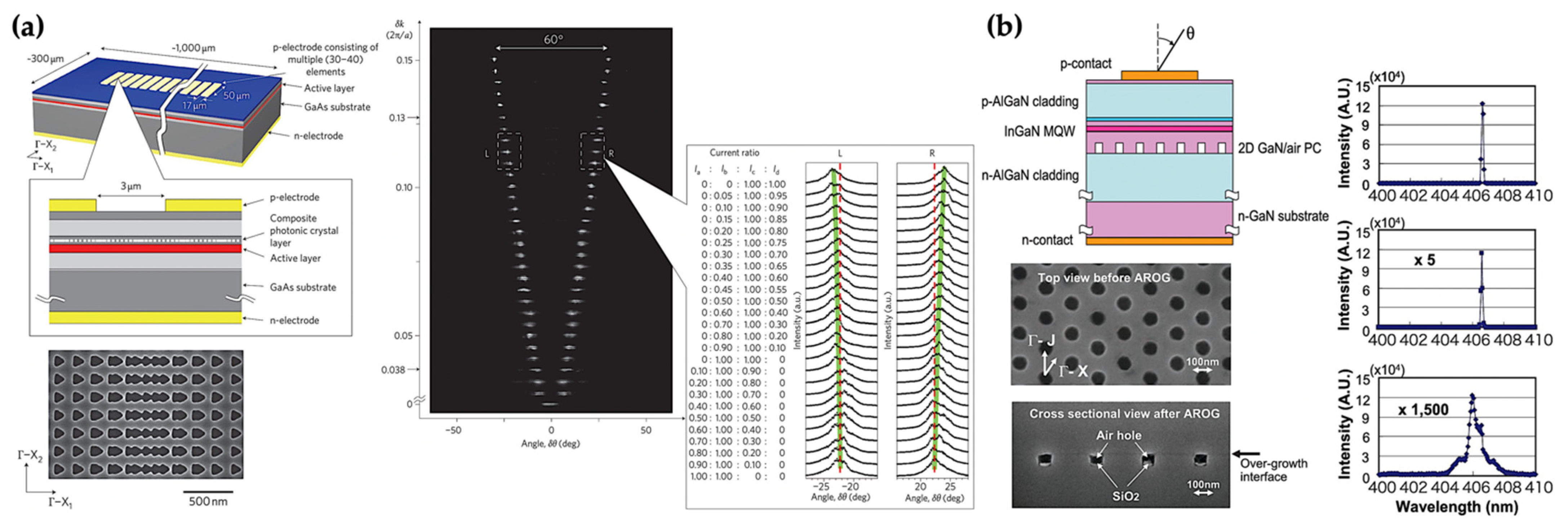
3.2. Light-Emitting Control and Emission Wavelength Expansion
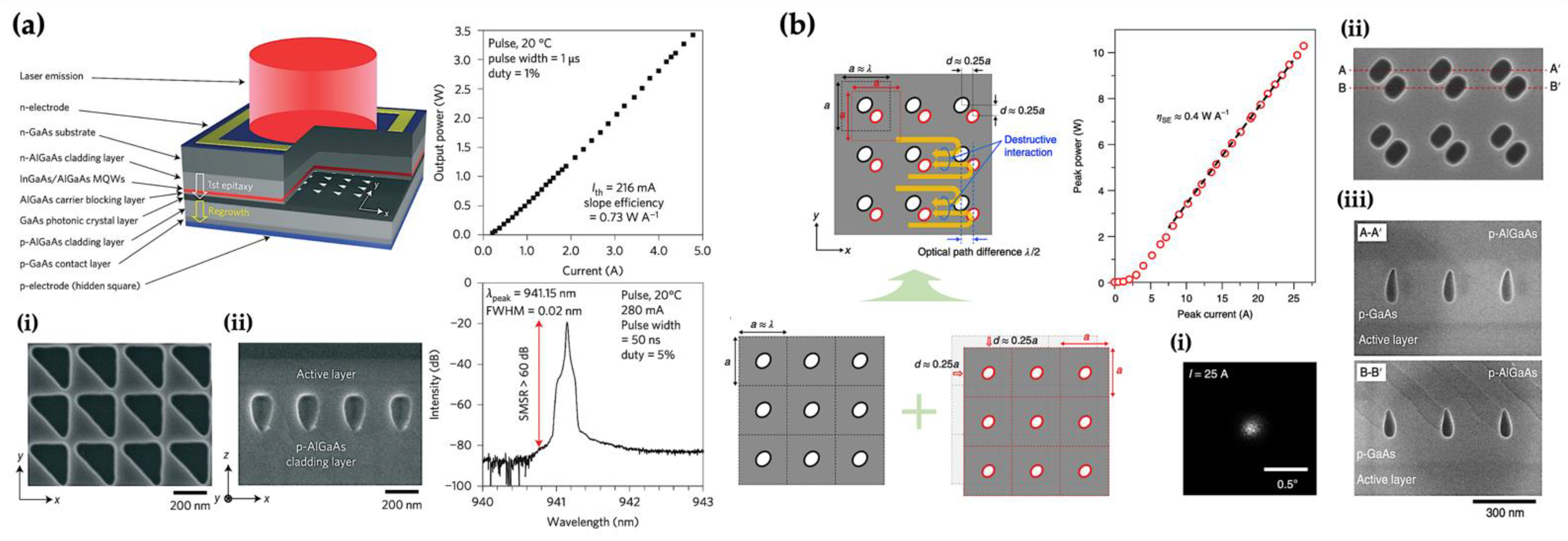
3.3. High-Power Operation with the Concept of Double-Lattice Structure
4. Toward a Lens-Free and Adjustment-Free ToF LiDAR System
4.1. Benchmark of PCSELs for ToF LiDAR System
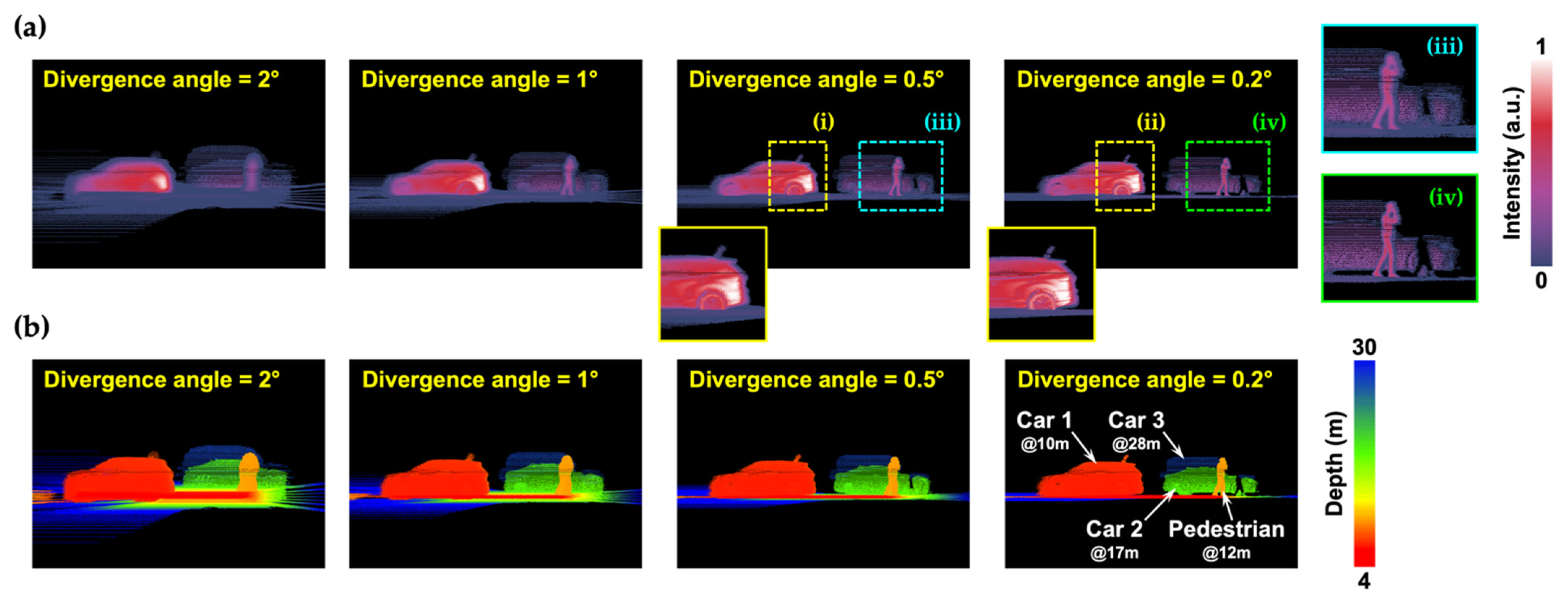
4.2. Real-Time Simulation and Visualisation via HELIOS
5. Conclusions
Author Contributions
Funding
Institutional Review Board Statement
Informed Consent Statement
Data Availability Statement
Acknowledgments
Conflicts of Interest
References
- 3D Imaging and Sensing-Technology and Market Trends 2021. Available online: https://www.i-micronews.com/products/3d-imaging-and-sensing-technology-and-market-trends-2021/ (accessed on 24 April 2022).
- Light Detection and Ranging (LiDAR) Market. Available online: https://www.fortunebusinessinsights.com/light-detection-and-ranging-lidar-market-101969 (accessed on 24 April 2022).
- Iga, K. Laboratory Notebook. March 1977. [Google Scholar]
- Iga, K.; Koyama, F.; Kinoshita, S. Surface emitting semiconductor lasers. IEEE J. Quantum Electron. 1988, 24, 1845–1855. [Google Scholar] [CrossRef]
- Iga, K. Surface-emitting laser-its birth and generation of new optoelectronics field. IEEE J. Sel. Top. Quantum Electron. 2000, 6, 1201–1215. [Google Scholar] [CrossRef]
- Iga, K. Vertical-cavity surface-emitting laser: Its conception and evolution. Jpn. J. Appl. Phys. 2008, 47, 1. [Google Scholar] [CrossRef]
- Iga, K. Vertical-cavity surface-emitting laser (VCSEL). Proc. IEEE 2013, 101, 2229–2233. [Google Scholar] [CrossRef]
- Koyama, F.; Kinoshita, S.; Iga, K. Room temperature cw operation of GaAs vertical cavity surface emitting laser. IEICE Trans. Electron. 1988, 71, 1089–1090. [Google Scholar]
- Larsson, A. Advances in VCSELs for communication and sensing. IEEE J. Sel. Top. Quantum Electron. 2011, 17, 1552–1567. [Google Scholar] [CrossRef]
- Moser, P.; Lott, J.A.; Bimberg, D. Energy efficiency of directly modulated oxide-confined high bit rate 850-nm VCSELs for optical interconnects. IEEE J. Sel. Top. Quantum Electron. 2013, 19, 1702212. [Google Scholar] [CrossRef]
- Pruijmboom, A.; Apetz, R.; Conrads, R.; Deppe, C.; Derra, G.; Gronenborn, S.; Gu, X.; Kolb, J.S.; Miller, M.; Moench, H.; et al. VCSEL arrays expanding the range of high-power laser systems and applications. J. Laser Appl. 2016, 28, 032005. [Google Scholar] [CrossRef]
- Ebeling, K.J.; Michalzik, R.; Moench, H. Vertical-cavity surface-emitting laser technology applications with focus on sensors and three-dimensional imaging. Jpn. J. Appl. Phys. 2018, 57, 08PA02. [Google Scholar] [CrossRef]
- Liu, A.; Wolf, P.; Lott, J.A.; Bimberg, D. Vertical-cavity surface-emitting lasers for data communication and sensing. Photonics Res. 2019, 7, 121–136. [Google Scholar] [CrossRef]
- Ishizaki, K.; De Zoysa, M.; Noda, S. Progress in photonic-crystal surface-emitting lasers. Photonics 2019, 6, 96. [Google Scholar] [CrossRef] [Green Version]
- Kalapala, A.; Song, A.; Pan, M.; Gautam, C.; Overman, L.; Reilly, K.; Rotter, T.; Balakrishnan, G.; Gibson, R.; Bedford, R.; et al. Scaling challenges in high power photonic crystal surface-emitting lasers. IEEE J. Quantum Electron. 2022. [Google Scholar] [CrossRef]
- Wang, Z.; Tong, C.; Wang, L.; Lu, H.; Tian, S.; Wang, L. Photonic crystal surface emitting laser operating in pulse-periodic regime with ultralow divergence angle. Photonics 2021, 8, 323. [Google Scholar] [CrossRef]
- Taylor, R.J.; Childs, D.; Hogg, R. Vector photonics: The commercial journey of PCSELs and their pathway to high power. In Proceedings of the SPIE High-Power Diode Laser Technology XX, San Francisco, CA, USA, 22 January–28 February 2022; Volume PC1198304. [Google Scholar]
- de Zoysa, M.; Inoue, T.; Yoshida, M.; Ishizaki, K.; Kunishi, W.; Gelleta, J.; Noda, S. Light detection functionality of photonic-crystal lasers. IEEE J. Quantum Electron. 2021, 57, 6400208. [Google Scholar] [CrossRef]
- Noda, S. Progress of photonic crystal surface-emitting lasers: Paradigm shift for lidar sensing and laser processing. In Proceedings of the Laser Resonators, Microresonators, and Beam Control XXIII, Virtual, 6–12 March 2021; Volume 11672, p. 1167203. [Google Scholar]
- Noda, S. Photonic crystal surface-emitting lasers and their application to lidar. In Proceedings of the 2021 26th Microoptics Conference (MOC), Hamamatsu, Japan, 26–29 September 2021; pp. 1–2. [Google Scholar]
- Yablonovitch, E. Inhibited spontaneous emission in solid-state physics and electronics. Phys. Rev. Lett. 1987, 58, 2059. [Google Scholar] [CrossRef] [Green Version]
- John, S. Strong localization of photons in certain disordered dielectric superlattices. Phys. Rev. Lett. 1987, 58, 2486. [Google Scholar] [CrossRef] [Green Version]
- Web of Science (WoS) Bibliometric Database. Available online: www.webofscience.com (accessed on 27 April 2022).
- Derwent Innovation’s Patent Database. Available online: www.derwentinnovation.com (accessed on 27 April 2022).
- Purcell, E.M. Spontaneous emission probabilities at radio frequencies. Phys. Rev. 1946, 69, 681. [Google Scholar]
- Heinzen, D.J.; Childs, J.J.; Thomas, J.E.; Feld, M.S. Enhanced and inhibited visible spontaneous emission by atoms in a confocal resonator. Phys. Rev. Lett. 1987, 58, 1320. [Google Scholar] [CrossRef]
- Hirayama, H.; Hamano, T.; Aoyagi, Y. Novel surface emitting laser diode using photonic band-gap crystal cavity. Appl. Phys. Lett. 1996, 69, 791–793. [Google Scholar] [CrossRef]
- Tandaechanurat, A.; Ishida, S.; Guimard, D.; Nomura, M.; Iwamoto, S.; Arakawa, Y. Lasing oscillation in a three-dimensional photonic crystal nanocavity with a complete bandgap. Nat. Photonics 2011, 5, 91–94. [Google Scholar] [CrossRef] [Green Version]
- Ryu, H.Y.; Notomi, M.; Lee, Y.H. High-quality-factor and small-mode-volume hexapole modes in photonic-crystal-slab nanocavities. Appl. Phys. Lett. 2003, 83, 4294–4296. [Google Scholar] [CrossRef] [Green Version]
- Takano, H.; Akahane, Y.; Asano, T.; Noda, S. In-plane-type channel drop filter in a two-dimensional photonic crystal slab. Appl. Phys. Lett. 2004, 84, 2226–2228. [Google Scholar] [CrossRef]
- Sugitatsu, A.; Asano, T.; Noda, S. Line-defect–waveguide laser integrated with a point defect in a two-dimensional photonic crystal slab. Appl. Phys. Lett. 2005, 86, 171106. [Google Scholar] [CrossRef]
- Nozaki, K.; Kita, S.; Baba, T. Room temperature continuous wave operation and controlled spontaneous emission in ultrasmall photonic crystal nanolaser. Opt. Express 2007, 15, 7506–7514. [Google Scholar] [CrossRef]
- Imada, M.; Noda, S.; Chutinan, A.; Tokuda, T.; Murata, M.; Sasaki, G. Coherent two-dimensional lasing action in surface-emitting laser with triangular-lattice photonic crystal structure. Appl. Phys. Lett. 1999, 75, 316–318. [Google Scholar] [CrossRef]
- Meier, M.; Mekis, A.; Dodabalapur, A.; Timko, A.; Slusher, R.E.; Joannopoulos, J.D.; Nalamasu, O. Laser action from two-dimensional distributed feedback in photonic crystals. Appl. Phys. Lett. 1999, 74, 7–9. [Google Scholar] [CrossRef]
- Imada, M.; Chutinan, A.; Noda, S.; Mochizuki, M. Multidirectionally distributed feedback photonic crystal lasers. Phys. Rev. B 2002, 65, 195306. [Google Scholar] [CrossRef]
- Dems, M.; Kotynski, R.; Panajotov, K. Planewave admittance method—A novel approach for determining the electromagnetic modes in photonic structures. Opt. Express 2005, 13, 3196–3207. [Google Scholar] [CrossRef] [PubMed]
- Drong, M.; Dems, M.; Perina, J.; Fordos, T.; Jaffres, H.Y.; Postava, K.; Drouhin, H.J. Time-dependent laser cavity perturbation theory: Exploring future nano-structured photonic devices in semi-analytic way. J. Lightwave Technol. 2022. [Google Scholar] [CrossRef]
- Dems, M. Convergence analysis of various factorization rules in the Fourier-Bessel basis for solving Maxwell equations using modal methods. Opt. Express 2021, 29, 4378–4391. [Google Scholar] [CrossRef] [PubMed]
- Frasunkiewicz, L.; Panajotov, K.; Thienpont, H.; Dems, M.; Czyszanowski, T. Transverse mode mixing in a coupled-cavity VCSEL. J. Lightwave Technol. 2020, 38, 5774–5782. [Google Scholar] [CrossRef]
- Kuc, M.; Piskorski, Ł.; Dems, M.; Wasiak, M.; Sokół, A.K.; Sarzała, R.P.; Czyszanowski, T. Numerical investigation of the impact of ITO, AlInN, plasmonic GaN and top gold metalization on semipolar green EELs. Materials 2020, 13, 1444. [Google Scholar] [CrossRef] [Green Version]
- Noda, S.; Kitamura, K.; Okino, T.; Yasuda, D.; Tanaka, Y. Photonic-crystal surface-emitting lasers: Review and introduction of modulated-photonic crystals. IEEE J. Sel. Top. Quantum Electron. 2017, 23, 1. [Google Scholar] [CrossRef]
- Sakai, K.; Miyai, E.; Noda, S. Coupled-wave model for square-lattice two-dimensional photonic crystal with transverse-electric-like mode. Appl. Phys. Lett. 2006, 89, 021101. [Google Scholar] [CrossRef]
- Sakai, K.; Miyai, E.; Noda, S. Coupled-wave theory for square-lattice photonic crystal lasers with TE polarization. IEEE J. Quantum Electron. 2010, 46, 788–795. [Google Scholar] [CrossRef] [Green Version]
- Liang, Y.; Peng, C.; Sakai, K.; Iwahashi, S.; Noda, S. Three-dimensional coupled-wave model for square-lattice photonic crystal lasers with transverse electric polarization: A general approach. Phys. Rev. B 2011, 84, 195119. [Google Scholar] [CrossRef] [Green Version]
- Yoshida, M.; De Zoysa, M.; Ishizaki, K.; Tanaka, Y.; Kawasaki, M.; Hatsuda, R.; Song, B.; Gelleta, J.; Noda, S. Double-lattice photonic-crystal resonators enabling high-brightness semiconductor lasers with symmetric narrow-divergence beams. Nat. Mater. 2019, 18, 121–128. [Google Scholar] [CrossRef] [PubMed]
- Koba, M.; Szczepański, P. Analysis of mode competition in a 2-D square lattice photonic crystal laser with transverse magnetic polarization. IEEE J. Quantum Electron. 2015, 51, 1–13. [Google Scholar] [CrossRef]
- Yang, Y.; Peng, C.; Liang, Y.; Li, Z.; Noda, S. Three-dimensional coupled-wave theory for the guided mode resonance in photonic crystal slabs: TM-like polarization. Opt. Lett. 2014, 39, 4498–4501. [Google Scholar] [CrossRef] [PubMed]
- Yang, Y.; Peng, C.; Li, Z. Semi-analytical approach for guided mode resonance in high-index-contrast photonic crystal slab: TE polarization. Opt. Express 2013, 21, 20588–20600. [Google Scholar] [CrossRef]
- Liang, Y.; Peng, C.; Ishizaki, K.; Iwahashi, S.; Sakai, K.; Tanaka, Y.; Kitamura, K.; Noda, S. Three-dimensional coupled-wave analysis for triangular-lattice photonic-crystal surface-emitting lasers with transverse-electric polarization. Opt. Express 2013, 21, 565–580. [Google Scholar] [CrossRef] [PubMed]
- Noda, S.; Yokoyama, M.; Imada, M.; Chutinan, A.; Mochizuki, M. Polarization mode control of two-dimensional photonic crystal laser by unit cell structure design. Science 2001, 293, 1123–1125. [Google Scholar] [CrossRef] [PubMed]
- Hong, Y.H.; Hsu, W.C.; Tsai, W.C.; Huang, Y.W.; Chen, S.C.; Kuo, H.C. Ultracompact nanophotonics: Light emission and manipulation with metasurfaces. Nanoscale Res. Lett. 2022, 17, 41. [Google Scholar] [CrossRef] [PubMed]
- Miyai, E.; Sakai, K.; Okano, T.; Kunishi, W.; Ohnishi, D.; Noda, S. Lasers producing tailored beams. Nature 2006, 441, 946. [Google Scholar] [CrossRef] [PubMed]
- Kitamura, K.; Nishimoto, M.; Sakai, K.; Noda, S. Needle-like focus generation by radially polarized halo beams emitted by photonic-crystal ring-cavity laser. Appl. Phys. Lett. 2012, 101, 221103. [Google Scholar] [CrossRef]
- Iwahashi, S.; Kurosaka, Y.; Sakai, K.; Kitamura, K.; Takayama, N.; Noda, S. Higher-order vector beams produced by photonic-crystal lasers. Opt. Express 2011, 19, 11963–11968. [Google Scholar] [CrossRef] [PubMed] [Green Version]
- Kurosaka, Y.; Iwahashi, S.; Liang, Y.; Sakai, K.; Miyai, E.; Kunishi, W.; Ohnishi, D.; Noda, S. On-chip beam-steering photonic-crystal lasers. Nat. Photonics 2010, 4, 447–450. [Google Scholar] [CrossRef]
- Ohnishi, D.; Okano, T.; Imada, M.; Noda, S. Room temperature continuous wave operation of a surface-emitting two-dimensional photonic crystal diode laser. Opt. Express 2004, 12, 1562–1568. [Google Scholar] [CrossRef]
- Kim, M.; Kim, C.S.; Bewley, W.W.; Lindle, J.R.; Canedy, C.L.; Vurgaftman, I.; Meyer, J.R. Surface-emitting photonic-crystal distributed-feedback laser for the midinfrared. Appl. Phys. Lett. 2006, 88, 191105. [Google Scholar] [CrossRef]
- Johnson, M.T.; Siriani, D.F.; Peun, T.M.; Choquette, K.D. Beam steering via resonance detuning in coherently coupled vertical cavity laser arrays. Appl. Phys. Lett. 2013, 103, 201115. [Google Scholar] [CrossRef] [Green Version]
- Siriani, D.F.; Choquette, K.D. Implant defined anti-guided vertical-cavity surface-emitting laser arrays. IEEE J. Quantum Electron. 2011, 47, 160–164. [Google Scholar] [CrossRef]
- Alias, M.S.; Shaari, S.; Leisher, P.O.; Choquette, K.D. Single transverse mode control of VCSEL by photonic crystal and trench patterning. Photonics Nanostructures Fundam. Appl. 2010, 8, 38–46. [Google Scholar] [CrossRef]
- Siriani, D.F.; Choquette, K.D. Electronically controlled two-dimensional steering of in-phase coherently coupled vertical-cavity laser arrays. IEEE Photonics Technol. Lett. 2010, 23, 167–169. [Google Scholar] [CrossRef]
- Gao, Z.; Thompson, B.J.; Dave, H.; Fryslie, S.T.; Choquette, K.D. Non-hermiticity and exceptional points in coherently coupled vertical cavity laser diode arrays. Appl. Phys. Lett. 2019, 114, 061103. [Google Scholar] [CrossRef]
- Kominis, Y.; Choquette, K.D.; Bountis, A.; Kovanis, V. Exceptional points in two dissimilar coupled diode lasers. Appl. Phys. Lett. 2018, 113, 081103. [Google Scholar] [CrossRef] [Green Version]
- Thompson, B.J.; Gao, Z.; Fryslie, S.T.; Choquette, K.D. Mode engineering in linear coherently coupled vertical-cavity surface-emitting laser arrays. IEEE J. Sel. Top. Quantum Electron. 2019, 25, 1701205. [Google Scholar] [CrossRef]
- Dave, H.; Gao, Z.; Fryslie, S.T.M.; Thompson, B.J.; Choquette, K.D. Static and dynamic properties of coherently-coupled photonic-crystal vertical-cavity surface-emitting laser arrays. IEEE J. Sel. Top. Quantum Electron. 2019, 25, 1700208. [Google Scholar] [CrossRef]
- Matsubara, H.; Yoshimoto, S.; Saito, H.; Jianglin, Y.; Tanaka, Y.; Noda, S. GaN photonic-crystal surface-emitting laser at blue-violet wavelengths. Science 2008, 319, 445–447. [Google Scholar] [CrossRef] [Green Version]
- Lu, T.C.; Chen, S.W.; Kao, T.T.; Liu, T.W. Characteristics of GaN-based photonic crystal surface emitting lasers. Appl. Phys. Lett. 2008, 93, 111111. [Google Scholar] [CrossRef]
- Bin, J.; Feng, K.; Shen, W.; Meng, M.; Liu, Q. Investigation on GaN-based membrane photonic crystal surface emitting lasers. Materials 2022, 15, 1479. [Google Scholar] [CrossRef] [PubMed]
- Choi, Y.S.; Hennessy, K.; Sharma, R.; Haberer, E.; Gao, Y.; DenBaars, S.P.; Nakamura, S.; Meier, C. GaN blue photonic crystal membrane nanocavities. Appl. Phys. Lett. 2005, 87, 243101. [Google Scholar] [CrossRef]
- David, A.; Fujii, T.; Moran, B.; Nakamura, S.; DenBaars, S.P.; Weisbuch, C.; Benisty, H. Photonic crystal laser lift-off GaN light-emitting diodes. Appl. Phys. Lett. 2006, 88, 133514. [Google Scholar] [CrossRef] [Green Version]
- Hong, K.B.; Chen, L.R.; Huang, K.C.; Yen, H.T.; Weng, W.C.; Chuang, B.H.; Lu, T.C. Impact of air-hole on the optical performances of epitaxially regrown p-side up photonic crystal surface-emitting lasers. IEEE J. Sel. Top. Quantum Electron. 2021, 28, 9479706. [Google Scholar] [CrossRef]
- Reuterskiöld Hedlund, C.; Martins De Pina, J.; Kalapala, A.; Liu, Z.; Zhou, W.; Hammar, M. Buried InP/air hole photonic-crystal surface-emitting lasers. Phys. Status Solidi A 2021, 218, 2000416. [Google Scholar] [CrossRef]
- McKenzie, A.F.; King, B.C.; Rae, K.J.; Thoms, S.; Gerrard, N.D.; Orchard, J.R.; Nishi, K.; Takemasa, K.; Sugawara, M.; Taylor, R.J.E.; et al. Void engineering in epitaxially regrown GaAs-based photonic crystal surface emitting lasers by grating profile design. Appl. Phys. Lett. 2021, 118, 021109. [Google Scholar] [CrossRef]
- Huang, Y.H.; Yang, Z.X.; Cheng, S.L.; Lin, C.H.; Lin, G.; Sun, K.W.; Lee, C.P. Effect of hole shift on threshold characteristics of gasb-based double-hole photonic-crystal surface-emitting lasers. Micromachines 2021, 12, 468. [Google Scholar] [CrossRef] [PubMed]
- Bian, Z.; Rae, K.J.; King, B.C.; Kim, D.; Li, G.; Thoms, S.; Childs, D.T.D.; Gerrard, N.D.; Babazadeh, N.; Reynolds, P.; et al. Comparative analysis of void-containing and all-semiconductor 1.5 µm InP-based photonic crystal surface-emitting laser diodes. AIP Adv. 2021, 11, 065315. [Google Scholar] [CrossRef]
- Chen, L.R.; Hong, K.B.; Huang, K.C.; Liu, C.L.; Lin, W.; Lu, T.C. Study of an epitaxial regrowth process by MOCVD for photonic-crystal surface-emitting lasers. Cryst. Growth Des. 2021, 21, 3521–3527. [Google Scholar] [CrossRef]
- Hirose, K.; Liang, Y.; Kurosaka, Y.; Watanabe, A.; Sugiyama, T.; Noda, S. Watt-class high-power, high-beam-quality photonic-crystal lasers. Nat. Photonics 2014, 8, 406–411. [Google Scholar] [CrossRef]
- Williams, D.M.; Groom, K.M.; Stevens, B.J.; Childs, D.T.; Taylor, R.J.; Khamas, S.; Hogg, R.A.; Ikeda, N.; Sugimoto, Y. Epitaxially regrown GaAs-based photonic crystal surface-emitting laser. IEEE Photonics Technol. Lett. 2012, 24, 966–968. [Google Scholar] [CrossRef]
- Hamamatsu Photonics, Photonic Crystal Surface Emitting Laser diodes (PCSEL). Available online: https://www.hamamatsu.com/jp/en.html (accessed on 23 April 2022).
- Inoue, T.; Morita, R.; Yoshida, M.; De Zoysa, M.; Tanaka, Y.; Noda, S. Comprehensive analysis of photonic-crystal surface-emitting lasers via time-dependent three-dimensional coupled-wave theory. Phys. Rev. B 2019, 99, 035308. [Google Scholar] [CrossRef]
- De Zoysa, M.; Yoshida, M.; Ishizaki, K.; Song, B.S.; Tanaka, Y.; Hatsuda, R.; Fukuhara, S.; Noda, S. 7W CW Operation of double-lattice photonic-crystal lasers. In Proceedings of the 2018 IEEE International Semiconductor Laser Conference (ISLC), Santa Fe, NM, USA, 16–19 September 2018; pp. 1–2. [Google Scholar]
- Iadanza, S.; Liles, A.A.; Butler, S.M.; Hegarty, S.P.; O’Faolain, L. Photonic crystal lasers: From photonic crystal surface emitting lasers (PCSELs) to hybrid external cavity lasers (HECLs) and topological PhC lasers. Opt. Mater. Express 2021, 11, 3245–3274. [Google Scholar] [CrossRef]
- Gao, X.; Yang, L.; Lin, H.; Zhang, L.; Li, J.; Bo, F.; Wang, Z.; Lu, L. Dirac-vortex topological cavities. Nat. Nanotechnol. 2020, 15, 1012–1018. [Google Scholar] [CrossRef] [PubMed]
- Wang, Z.; Liang, Y.; Beck, M.; Scalari, G.; Faist, J. Topological charge of finite-size photonic crystal modes. Phys. Rev. B 2020, 102, 045122. [Google Scholar] [CrossRef]
- Yoshida, M.; De Zoysa, M.; Ishizaki, K.; Kunishi, W.; Inoue, T.; Izumi, K.; Hatsuda, R.; Noda, S. Photonic-crystal lasers with high-quality narrow-divergence symmetric beams and their application to LiDAR. J. Phys. Photonics 2021, 3, 022006. [Google Scholar] [CrossRef]
- Morita, R.; Inoue, T.; De Zoysa, M.; Ishizaki, K.; Noda, S. Photonic-crystal lasers with two-dimensionally arranged gain and loss sections for high-peak-power short-pulse operation. Nat. Photonics 2021, 15, 311–318. [Google Scholar] [CrossRef]
- Takagi, S.; Tanimura, H.; Kakuno, T.; Hashimoto, R.; Kaneko, K.; Saito, S. Evaluation of thermal resistance of surface-emitting quantum cascade laser using structural function and 3D thermal flow simulation. In Proceedings of the 9th International Conference on Photonics, Optics and Laser Technology (PHOTOPTICS 2021), Online Streaming, 11–13 February 2021; pp. 88–93. [Google Scholar]
- Guo, X.; Wang, Y.; Qi, A.; Qi, F.; Zhang, S.; Zheng, W. Photonic crystal surface emitting laser with ultralow thermal resistance and narrow divergence angle. In Proceedings of the 2016 Conference on Lasers and Electro-Optics (CLEO), San Jose, CA, USA, 5–10 June 2016. [Google Scholar]
- Sciancalepore, C.; Bakir, B.B.; Seassal, C.; Letartre, X.; Harduin, J.; Olivier, N.; Fedeli, J.M.; Viktorovitch, P. Thermal, modal, and polarization features of double photonic crystal vertical-cavity surface-emitting lasers. IEEE Photonics J. 2012, 4, 399–410. [Google Scholar] [CrossRef]
- Haghighat, G.; Ahmadi, V. Analysis of SHB and thermal characteristics in PC-VCSEL considering photonic crystal parameters. In Proceedings of the OSA Asia Communications and Photonics Conference, Shanghai, China, 13–16 November 2011; Volume 83082G. [Google Scholar]
- Czyszanowski, T. Thermal properties and wavelength analysis of telecom oriented photonic-crystal VCSELs. Opto-electron. Rev. 2010, 18, 56–62. [Google Scholar] [CrossRef]
- De Zoysa, M.; Yoshida, M.; Song, B.; Ishizaki, K.; Inoue, T.; Katsuno, S.; Izumi, K.; Tanaka, Y.; Hatsuda, R.; Gelleta, J.; et al. Thermal management for CW operation of large-area double-lattice photonic-crystal lasers. JOSA B 2020, 37, 3882–3887. [Google Scholar] [CrossRef]
- Noda, S.; Yoshida, M.; Kunishi, W.; Inoue, T.; Ishizaki, K.; De Zoysa, M.; Kitamura, K.; Shimaji, N.; Nishimura, K. Photonic crystal lasers: Fabrication with AI-assisted technology and application to LiDAR system. AI Opt. Data Sci. II SPIE 2021, 11703, 117030M. [Google Scholar]
- HELIOS++-Heidelberg LiDAR Operations Simulator. Available online: https://www.geog.uni-heidelberg.de/gis/helios.html (accessed on 28 April 2022).
- Ito, K.; Niclass, C.; Aoyagi, I.; Matsubara, H.; Soga, M.; Kato, S.; Maeda, M.; Kagami, M. System design and performance characterization of a mems-based laser scanning time-of-flight sensor based on a 256 × 64-pixel single-photon imager. IEEE Photonics J. 2013, 5, 6800114. [Google Scholar] [CrossRef]
- Alda, J. Laser and Gaussian beam propagation and transformation. Encycl. Opt. Eng. 2003, 999–1013. [Google Scholar]


| Year | 2014 [77] | 2019 [45] | 2021 [85] | 2021 [86] |
| Lattice | Square lattice Isosceles right triangle | Square lattice Double hole | Square lattice Double hole | Square lattice Double hole |
| Structure (µm) | n-side up, 200 | n-side up, 500 | n-side up, 500 | n-side up, 400 or 1000 |
| Extra design | NA | NA | w/p-side DBR | w/loss section |
| Operation mode | Pulsed mode @20 °C pulse width = 1 μs, duty cycle = 1% | Pulsed mode @200 Hz, pulse width = 200 ns | Pulsed mode @1 kHz, pulse width 100 ns | Pulsed mode @1.1 GHz, pulse width ~ 35 ps |
| CW mode @20 °C | CW mode @5–20 °C | |||
| Threshold current (A) | 0.216 | 2 | 2.1 | NA |
| 0.22 | 3.3 | |||
| Slope efficiency (W/A) | 0.73 | 0.4 | 0.8 | NA |
| 0.66 | 0.48 | |||
| Maximum power (W) | 3.4 @5 A (limited by driver) | >10 @25 A | >10 @15 A | 20 @3–4 A @1 GHz, pulse width ~ 35 ps 300 @30 A @1 GHz, pulse width ~ 40 ps |
| 1.5 @2.5 A | 7 | |||
| Divergence angle | <1° | <0.3° @10 W | 0.17° @10 W | 0.35° |
| <3° @1.5 W | NA | NA | NA |
Publisher’s Note: MDPI stays neutral with regard to jurisdictional claims in published maps and institutional affiliations. |
© 2022 by the authors. Licensee MDPI, Basel, Switzerland. This article is an open access article distributed under the terms and conditions of the Creative Commons Attribution (CC BY) license (https://creativecommons.org/licenses/by/4.0/).
Share and Cite
Hong, Y.-H.; Miao, W.-C.; Hsu, W.-C.; Hong, K.-B.; Lin, C.-L.; Lin, C.; Chen, S.-C.; Kuo, H.-C. Progress of Photonic-Crystal Surface-Emitting Lasers: A Paradigm Shift in LiDAR Application. Crystals 2022, 12, 800. https://doi.org/10.3390/cryst12060800
Hong Y-H, Miao W-C, Hsu W-C, Hong K-B, Lin C-L, Lin C, Chen S-C, Kuo H-C. Progress of Photonic-Crystal Surface-Emitting Lasers: A Paradigm Shift in LiDAR Application. Crystals. 2022; 12(6):800. https://doi.org/10.3390/cryst12060800
Chicago/Turabian StyleHong, Yu-Heng, Wen-Chien Miao, Wen-Cheng Hsu, Kuo-Bin Hong, Chun-Liang Lin, Ching Lin, Shih-Chen Chen, and Hao-Chung Kuo. 2022. "Progress of Photonic-Crystal Surface-Emitting Lasers: A Paradigm Shift in LiDAR Application" Crystals 12, no. 6: 800. https://doi.org/10.3390/cryst12060800