1. Introduction
After decades of vigorous development of microelectronics technology, up to now, silicon materials have gradually penetrated into the fields of optical detection, optical communication, solar cells, and so on, becoming the cornerstone of the semiconductor industry because of their mature technology and rich reserves. With the continuous expansion of the silicon application field, efforts to improve the properties of silicon have become essential. In the 21st century, micro/nanofabrication technology shines brilliantly in the fields of information science, aerospace, and engineering materials, promoting the realization of many new functional electronic and photonic devices [
1]. Micro/nanostructured silicon has also emerged under this background, greatly improving the optical and electrical characteristics of silicon [
2,
3]. Due to the light trapping effect on the surface of micro/nanostructured silicon, the surface reflectance of single crystalline silicon can be reduced to about 10% [
4]. In recent years, it has been reported that surface micro/nanostructured silicon can be obtained by different methods, such as alkaline etching [
5,
6], metal-assisted chemical etching [
7,
8], and ultrafast laser pulse processing [
9,
10,
11,
12]. In particular, impurity elements such as S, Se, and Te can be introduced into the silicon lattice when an ultrafast laser pulse interacts with silicon [
10,
11,
12]. Theoretically [
13] and experimentally [
14], it has been demonstrated that chalcogen-doped (S, Se, Te) silicon can introduce an intermediate band energy level in the silicon band gap that is conducive to sub-bandgap absorption, further enhancing the effectiveness and photoelectric response of silicon-based photodetectors. The chalcogen-doped microstructured silicon thus breaks through the limitations of commercially available silicon-based optoelectronic devices, making silicon materials potentially useful in the field of infrared detectors [
15], or is expected to improve the efficiency of silicon solar cells [
16]. However, femtosecond laser irradiation induces sharp conical spikes on the silicon surface and leaves some lattice defects simultaneously, which are not conducive to the fabrication of optoelectronic devices for CMOS process. In addition, surface morphology, dopant distribution, and impurity energy levels will vary due to different laser processing parameters when the laser pulse interacts with silicon, thereby affecting photoelectric conversion efficiency.
In this paper, we explored the differences in the surface structure, impurity distribution, crystal phase, and near-infrared photocurrent response of Se-doped silicon prepared by fs laser and ps laser, respectively, and discussed the reasons for these differences based on the dopant incorporation mechanism of the laser processing of semiconductors. In this paper, we find ps laser induces less damage to the silicon lattice than the fs laser, and the selenium distribution on the surface of ps-laser-treated Si is more compact. Analysis of near-infrared photocurrent results revealed that a higher doping concentration contributes to a higher near-infrared photocurrent response.
2. Experimental
In the experiments, the Si–Se bilayer film-coated silicon samples were fabricated as follows. Firstly, N-type single-polished Si wafers ((100) orientation, 8–10 Ω cm, 520 μm thick) were cleaned by RCA standard cleaning procedure with each step for 15 min to remove organic and metallic contaminants [
17]. A 100 nm-thick Se film was thermally evaporated onto the cleaned Si wafers. A 150 nm-thick Si film was then deposited on the surface of Se film by magnetic sputtering in order to protect some dopants from evaporating during laser processing [
17]. As shown in
Figure 1, the Si–Se-coated silicon sample was placed on sample stage exposed to the atmosphere and mounted on a computer-controlled three-dimensional translation stage, then scanned line by line using fs laser [
17] and ps laser, respectively, in a raster manner. A Ti: sapphire amplifier laser (
λ = 800 nm,
τ = 100 fs,
f = 1000 Hz) and a fiber ps laser (
λ = 1064 nm,
τ = 8.7 fs,
f = 2000 kHz) were used successively to irradiate Si with an average of 200 pulses at normal incidence. According to the monitoring of Gaussian beam profile by a CCD camera, the fs laser pulses and ps laser pulses have full-width half maximum of 200 μm and 20 μm (FWHM of a Gaussian beam) after focused by convex lens, achieving an average fluence of 4.5 kJ/m
2 and 1.4 kJ/m
2 for each pulse, respectively. Average fluence
can be calculated by the following formula
, where
P,
f, and
D represent the average power, laser repetition frequency, and diameter of the laser spot, respectively. In order to ensure the exposed Si surface receives uniform laser exposure, the distance between adjacent scanning lines during laser processing was designed to be 200 μm and 20 μm for fs laser and ps laser, respectively.
After fs laser and ps laser treatment, the samples were washed in an ultrasonic bath of acetone for 10 min to remove any powder remaining on the surface. A Hitachi SU8010 field emission scanning electron microscope (FESEM) was used to investigate the sample morphology of structural modifications. Atom force microscope (AFM, Digital Instruments, Dimenson Icon) was used to analyze the surface roughness of the processed samples. Field scanning SEM, in combination with energy dispersive (X-ray) spectroscopy (EDX), was used to detect the selenium element and map the Se distribution. The crystallinity of the laser-processed samples was characterized using Thermo’s DXR Raman microscope in backscattering geometry with 780 nm laser at a power of 5.1 mW. Finally, samples were annealed at 773 K for 1 h in a tube furnace under flowing nitrogen, then were used to fabricate Se-doped silicon N
+-N photodiode according to the method in [
14]. Photoelectric response of the photodiodes in near-infrared band was studied using Fourier transform infrared spectroscopy (FTIR) combined with chopper and an external lock-in amplifier.
3. Experimental Results and Discussion
In order to reveal the influence of laser pulse parameters on the processing results of the microstructures, the fs-laser-treated and ps-laser-treated surface morphologies are shown in
Figure 2 for comparison. It can be observed that quasi-ordered micron-size columnar structures, along with some deeper gullies, can be formed after fs laser processing of Si coated with Se film. For the case of ps laser processing, the surface morphologies are identified as cavities and irregular nanoscale spherical particles. Here, for a more detailed comparison, the surface morphologies of the fs-laser-treated and ps-laser-treated samples were further characterized by AFM to obtain a morphological comparison in detail.
Figure 3 shows the AFM photographs obtained for the samples with a scale of 5 × 5 μm. The root mean square (rms) roughness for the fs-laser-treated sample and the ps-laser-treated sample are ~478 nm and ~122 nm, respectively. The maximum height of the fs-laser-formed columnar structure is about 3225 nm, and the maximum height of the ps-laser-formed nanospikes is about 889 nm.
With the same number of incident laser pulses, the large variation in surface morphologies obtained involves different pulse duration, laser fluence and wavelength. Melting, ablation, and microstructure self-organization formation take place successively during the laser interaction with the silicon [
18]. With higher average fluence and wider spot size in diameter, fs laser deposit more energy to the sample surface, resulting heat diffusion into the processed-area is wider and deeper. The difference in energy density and spot diameter causes a difference in the volume of the ablation material. Fs laser ablate away larger volume of silicon to form the resulting 3–4 μm tall columnar structures, however, ps laser can only ablate away the silicon at the shallower surface to form the resulting nano-scale spherical particles. A series of processes of energy deposition, thermal melting and molten layer redepositon can be completed for fs laser treatment on a timescale faster than the ps laser treatment [
19]. As a result, fs laser processing of silicon has the characteristics of higher spatial resolution and less thermal damage to the processed-area periphery [
3]. The dependence of machining characteristics on pulse width can explain why the surface morphologies processed by fs laser are more regular and smoother than those processed by ps laser.
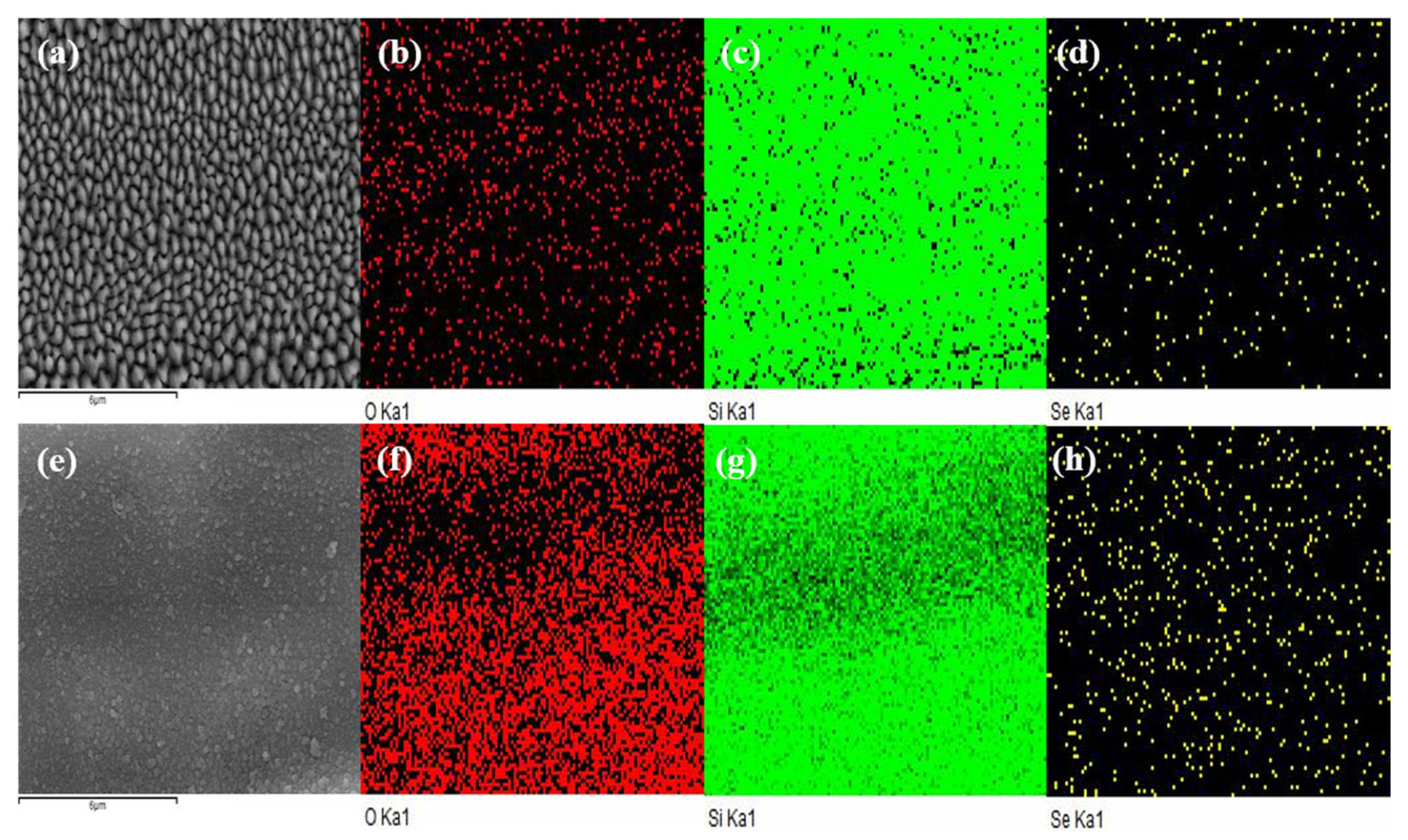
For a demonstration of the incorporation of selenium atoms during laser pulse irradiating silicon in the presence of dopant precursors, SEM-EDX (
Figure 4) of the convex position in micro/nanostructures was taken in spot mode in the same positions marked by the pointer in
Figure 2b and
Figure 3d. In order to highlight the selenium peak, the insets in
Figure 4 are enlarged to show the EDX counts between 0.8 KeV to 1.6 KeV. Obviously, the presence of selenium is confirmed. Six repeated measurements of different points and EDX quantitative analysis show that the selenium concentration of the fs-laser-processed sample is higher than that of the ps-laser-processed sample, and both of them are close to the resolution limit of EDX on the order of 1%. Then, SEM-EDX of the two laser-treated samples was taken in surface scanning mode for the areas in
Figure 5a,e to investigate the distribution of selenium. The maps of oxygen, silicon, and selenium for fs-laser-treated silicon and ps-laser-treated silicon are shown in
Figure 5b–d and
Figure 5f–h, respectively.
Figure 5b,f shows that oxygen is present on the sample surface, and the distribution of oxygen is approximately complementary to that of silicon, indicating the micro/nanostructures of the two samples are mainly composed of SiO
x, which reveals that oxidation occurs during laser pulse processing.
Figure 5d,h for the Se maps shows a difference in selenium distribution between the fs-laser-treated and ps-laser-treated silicon surfaces. Obviously, the selenium distribution on the surface of ps-laser-treated Si is more compact, indicating a higher doping concentration of selenium in ps-laser-processed silicon. This could be ascribed to fs lasers ablation of a larger volume of silicon, leaving deep and wide micron-scale gullies between the cylinder structures. Previous studies have shown that chalcogen dopants can be incorporated into the topmost 300 nm of silicon by laser irradiation on Si coated with chalcogen thin film [
20]. It is considered that impurity atoms are mainly distributed on the surface of the convex cylinder structure, and there is almost no selenium distributed in the gully between the cylinders. However, EDX detection in spot mode showed a lower dopant concentration of ps-laser-treated silicon than that of fs-laser-treated silicon. Dopants can be introduced into silicon using laser pulse irradiating as an evaporated thin film, and the hyper-doping mechanism is that molten liquid can contain more dopants than the solid phase in equilibrium [
3]. Due to the higher average fluence of the fs laser pulse, the fs laser pulse accumulatively deposits more energy than the ps laser pulse after the same number of pulse radiations. The more energy is deposited, the deeper the heat diffuses into the processing area and converts it into a molten layer. The molten layer enables dopants to diffuse in and traps more dopants in silicon, resulting in higher Se atom counts in the microregion.
Then, for further investigation of the crystalline properties of the fs-laser-processed and ps-laser-processed regions, Raman analysis was conducted with a spectral resolution of less than 2 cm
−1.
Figure 6 shows the Raman spectra for fs-laser-processed silicon (solid blue line) and ps-laser-processed silicon (pink dashed line). It can be observed from
Figure 6 that there is only one sharp spectral peak for the ps-treated sample at 520 cm
−1, which is evidence of the single-crystal phase corresponding to the original diamond structure (Si-I). However, for the fs-laser-treated silicon, besides the sharp Raman peak at 520 cm
−1, the Raman spectra show broadband peaks centered at 470 cm
−1, which is characteristic of amorphous silicon (α-Si) [
21]. The simultaneous appearance of two peaks at 520 cm
−1 and t 470 cm
−1 demonstrates that the mixed phase silicon of Si-I and α-Si exists in the fs-laser-treated sample. The formation of amorphous silicon could be attributed to the structural instability caused by laser pulse radiation and silicon doping beyond the solubility limit [
22]. Compared with ps laser pulses, the fs laser pulses generate large peak electric fields [
3], which break the bonds of the atoms to electrons and are more likely to excite the instability of the lattice structure. In addition, the fs laser pulse interacts with silicon on a timescale shorter than the electron–phonon coupling relaxation time [
3]. Most of the laser energy is absorbed by electrons and leaves the ions completely “cold”, resulting in a change in the lattice structure. Moreover, the EDX counts in
Figure 4 show a higher dopant concentration in the microregions of fs-treated Si, meaning a greater probability of lattice damage. This indicates that the doped layer produced by ps laser radiation has better crystallinity than that produced by fs laser radiation.
The above results show that the ps laser produces a Se-doped layer with a higher dopant concentration than the fs-laser-produced Se-doped layer over a larger area, albeit at a lower dopant concentration in the microregion. Chalcogenide doping concentration will affect the sub-bandgap absorption while increasing the doping concentration is beneficial to obtain more sub-bandgap absorption [
3], thereby improving device performance. To compare the optoelectronic properties of fs-laser-produced Se-doped Si and ps-laser-produced Se-doped Si, we tested the photocurrent response spectra of N
+-N junction photodiodes fabricated from these two materials in the near-infrared band from 1.1 to 2.5 μm, as shown in
Figure 7. Before fabricating the diodes, both the two materials were annealed at 773 K for 1 h to ensure optimal rectification characteristics and eliminate the influence of the amorphous silicon structure. Hall measurements (Lake Shore 8400) show that the bulk electron concentration of fs-laser-treated Si and ps-laser-treated Si are 3.57 × 10
14 cm
−3 and 1.49 × 10
15 cm
−3, respectively, and both are higher than that of the substrate with 2.8 × 10
13 cm
−3. As a result,
Figure 7 shows that the photocurrent intensities of the two photodiodes over the range 1.1–1.2 μm are basically the same, and the absorption of photons in this range is independent of selenium doping and depends on the band gap of intrinsic silicon. For the wavelength from 1.2 to 2.5 μm, the photocurrent of the ps-laser-treated silicon diode is greater than that of the fs-laser-treated diode; this can be ascribed to a higher dopant concentration of ps-treated Si with more sub-band absorption.


