
Surface Dispersion Suppression in High-Frequency GaN Devices
Abstract
:1. Introduction
2. Surface States and Virtual Gate
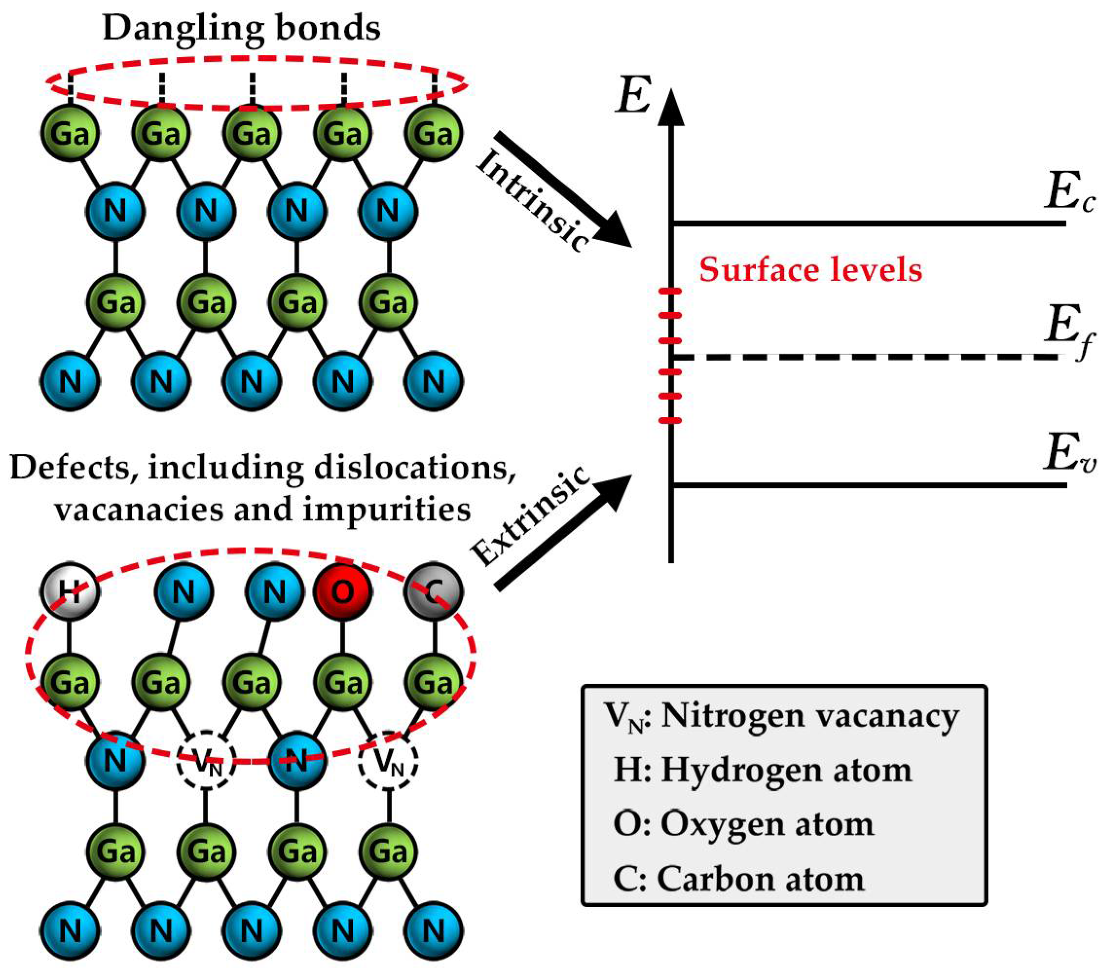
2.1. Sources of Surface States
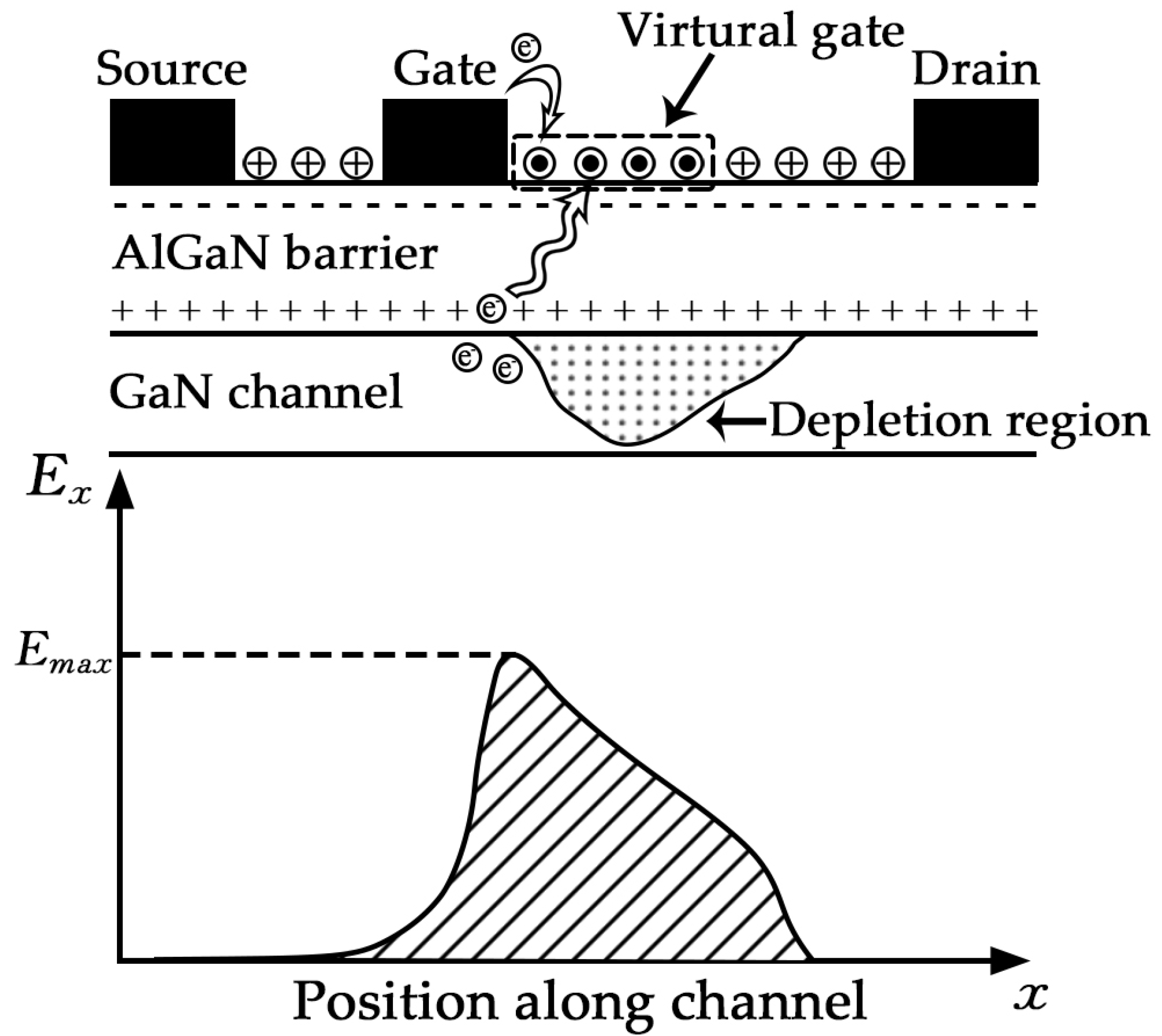
2.2. Virtual Gate Model
3. Methods for Suppression Surface Dispersion and Their Bottlenecks
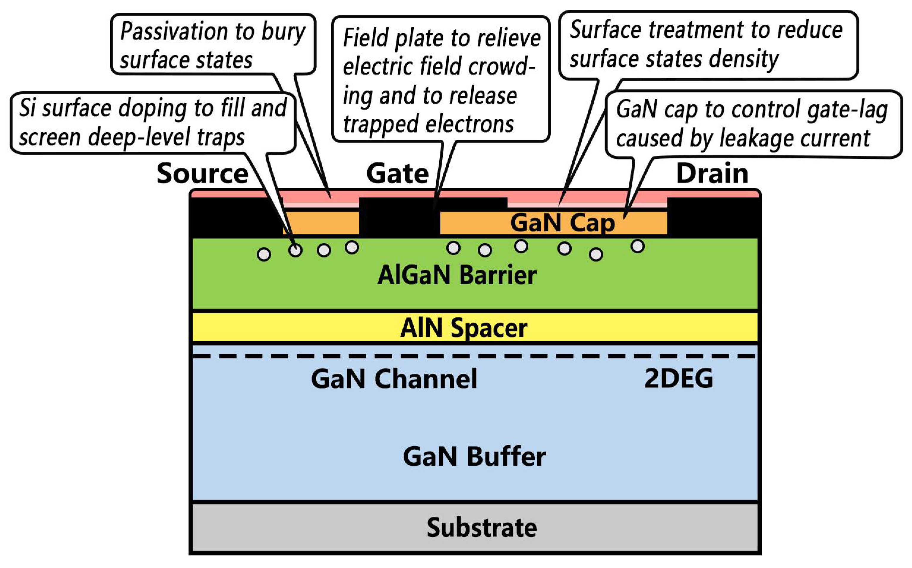
3.1. Common Methods for Suppression Surface Dispersion
3.1.1. Surface Treatment
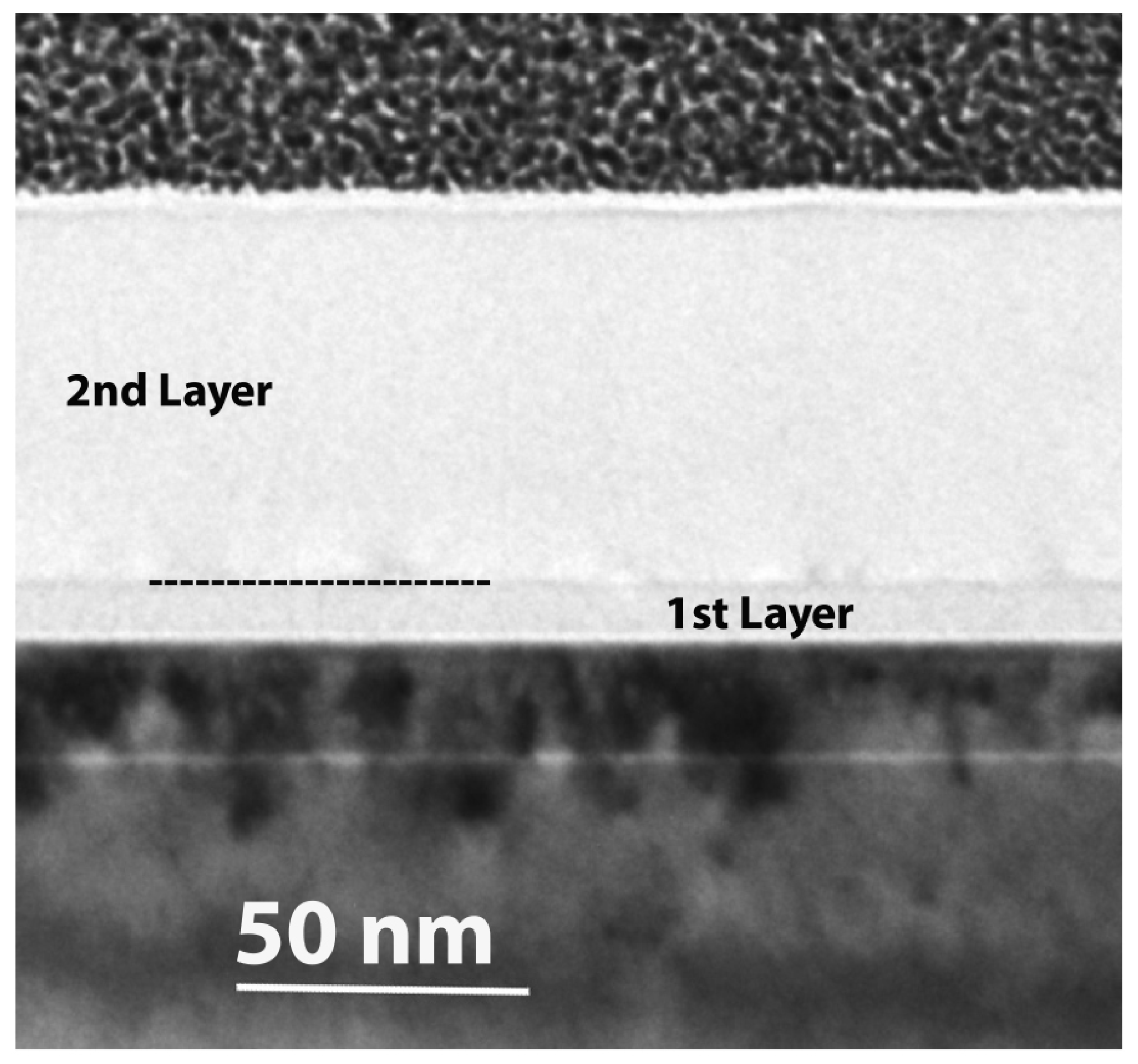
3.1.2. Passivation
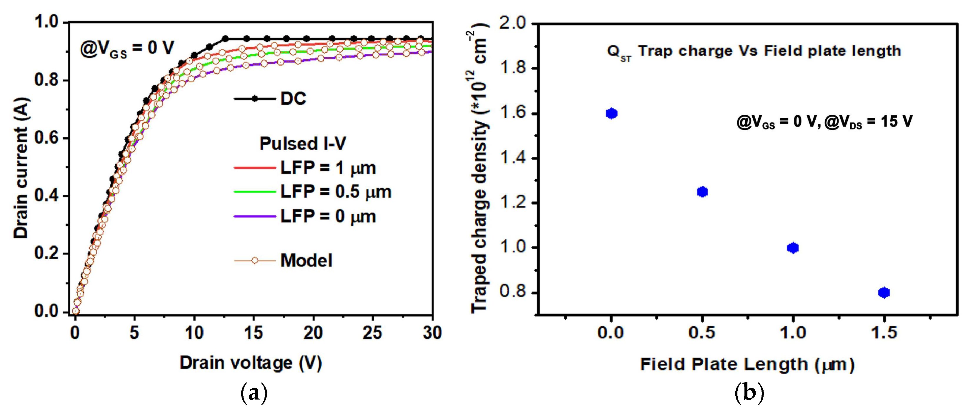
3.1.3. Field Plate
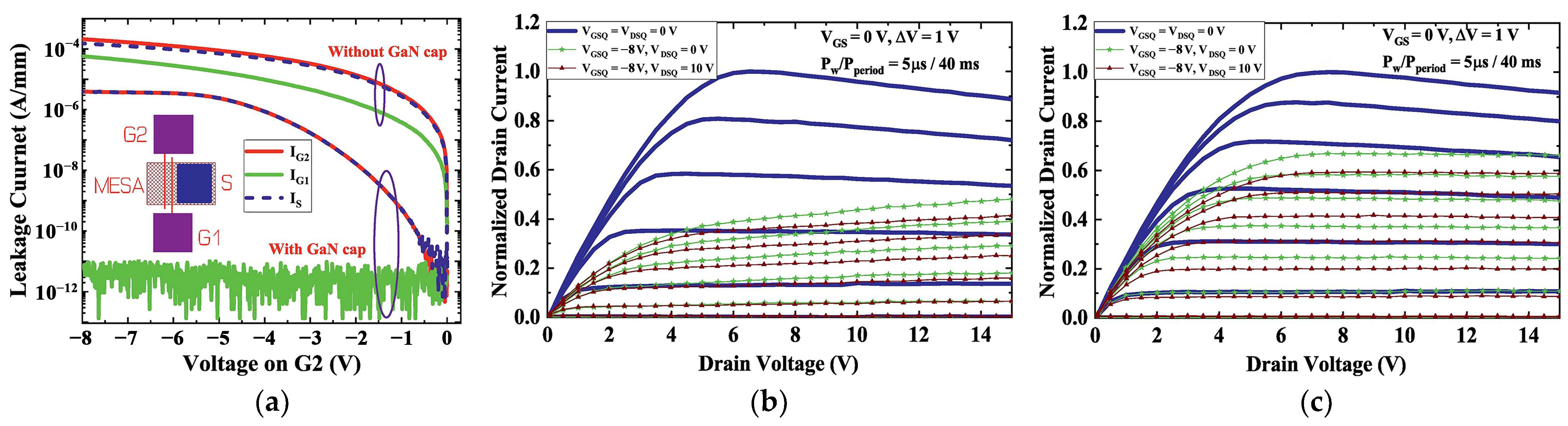
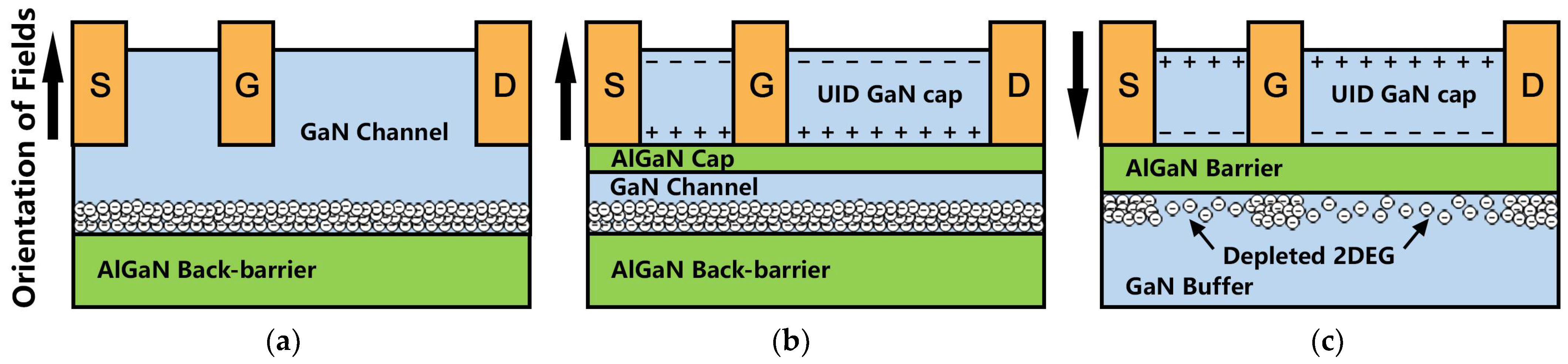
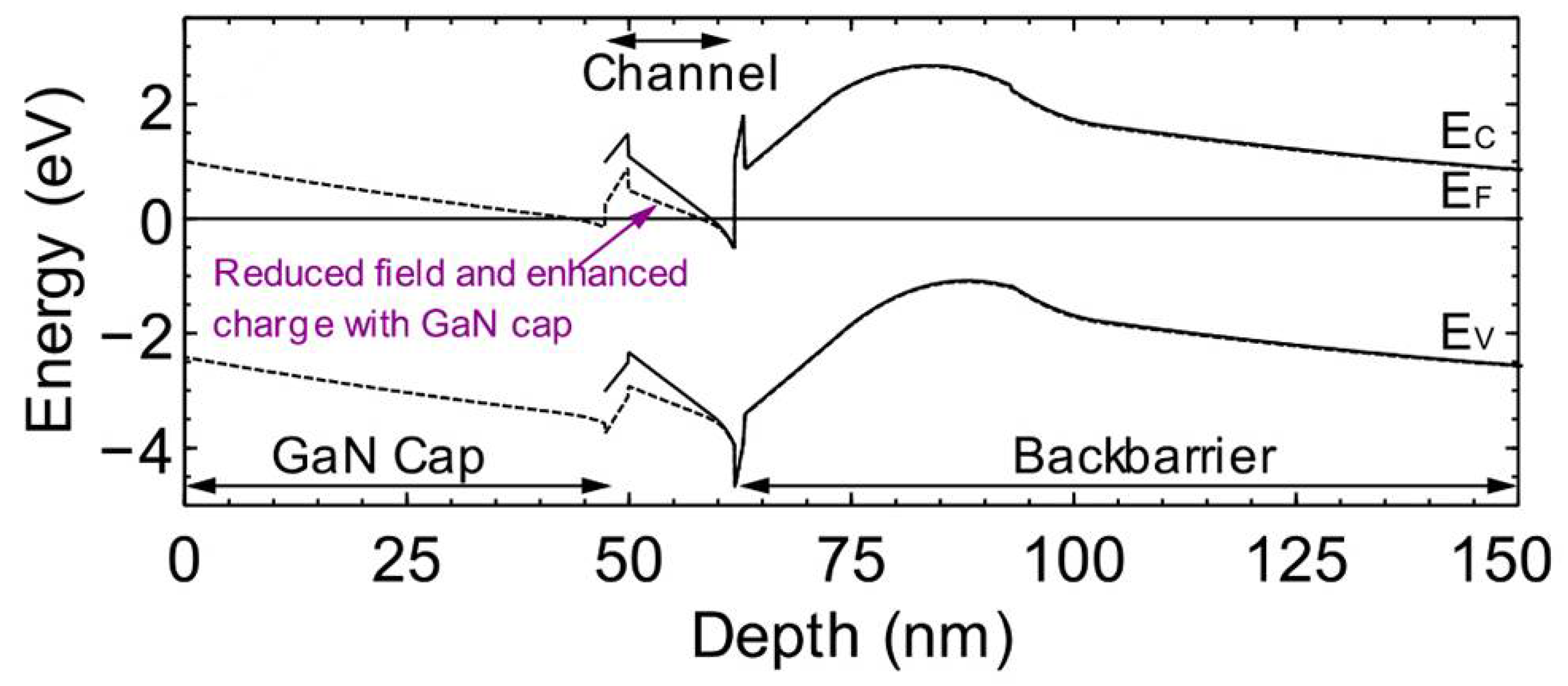
3.1.4. GaN Cap
3.1.5. Si Surface Doping
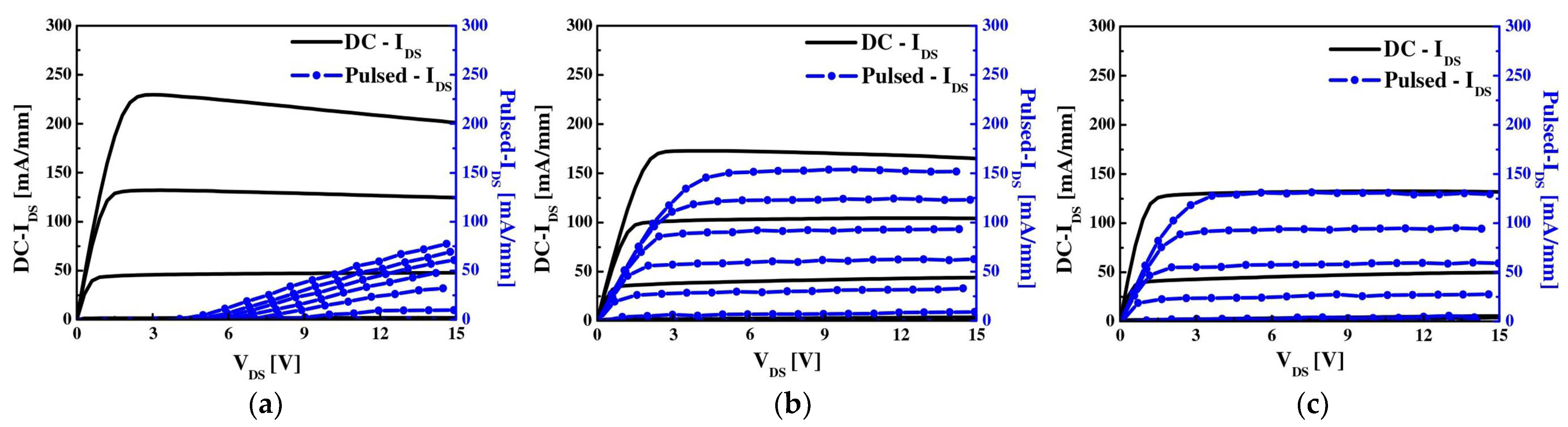
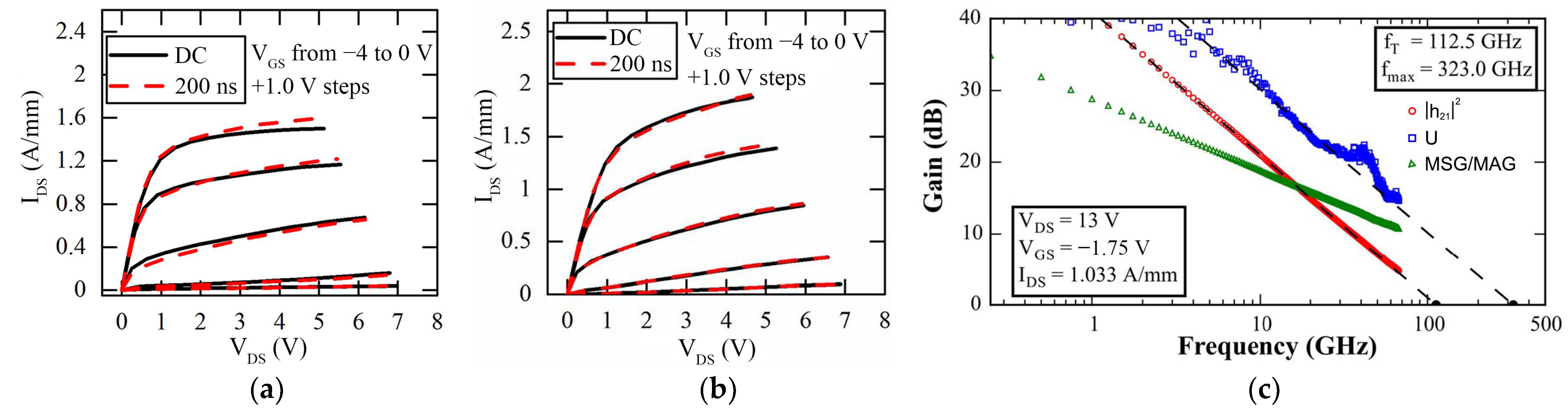
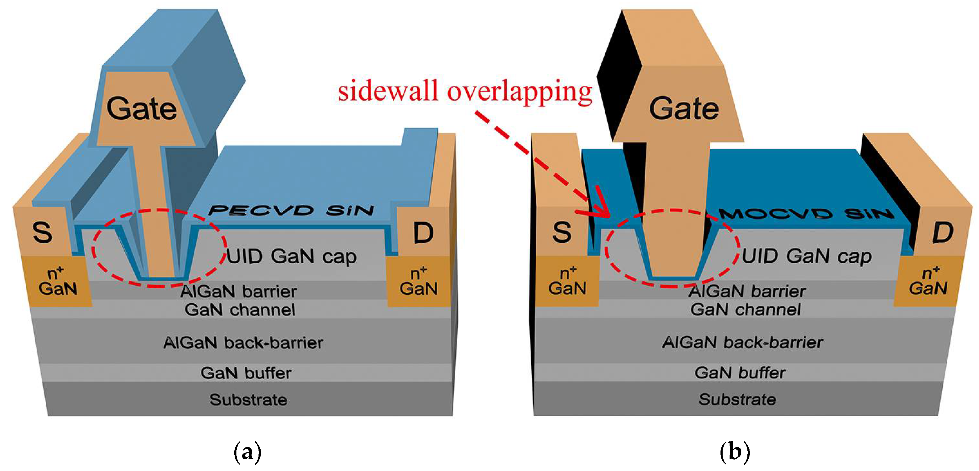
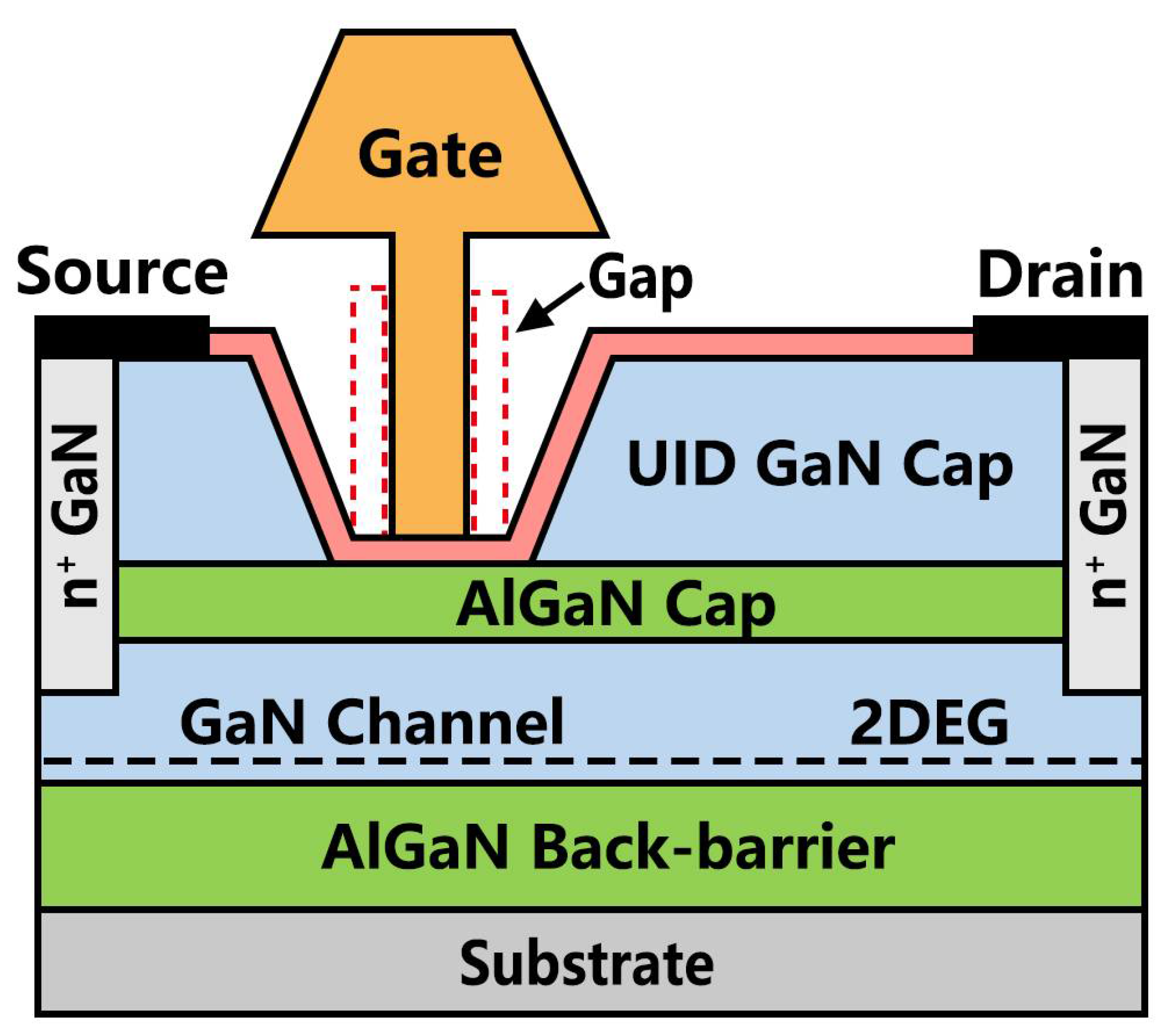
3.2. Bottlenecks Encountered at High Frequencies
4. NPDR MIS-HEMTs for High-Frequency Device
4.1. What and Why Is NPDR?
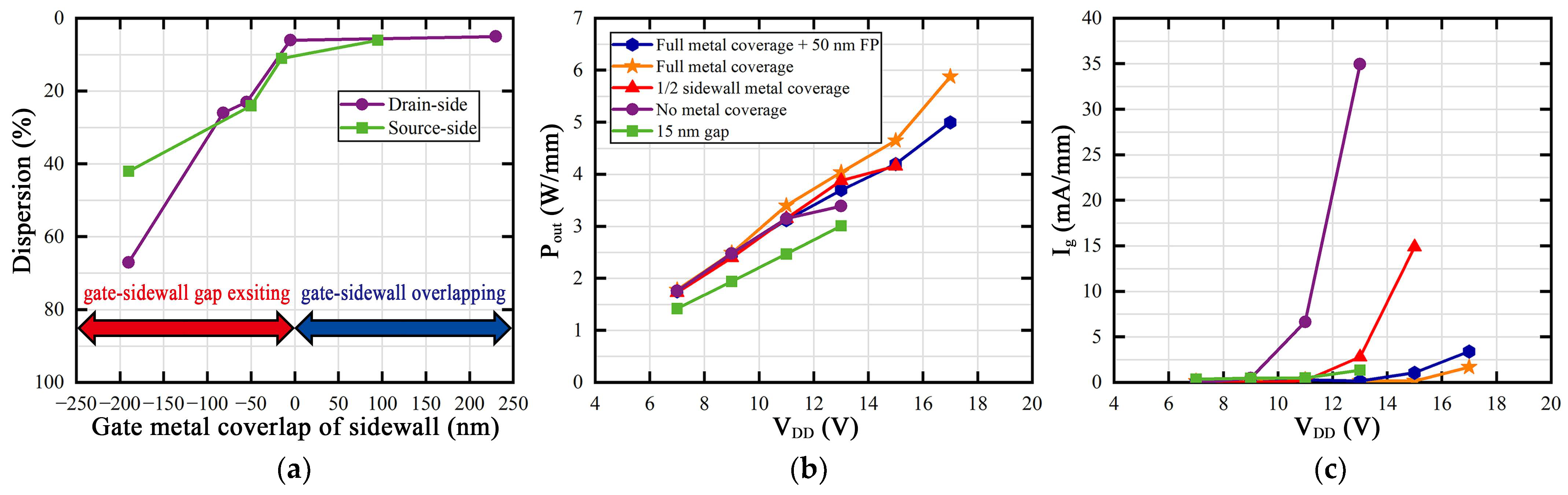
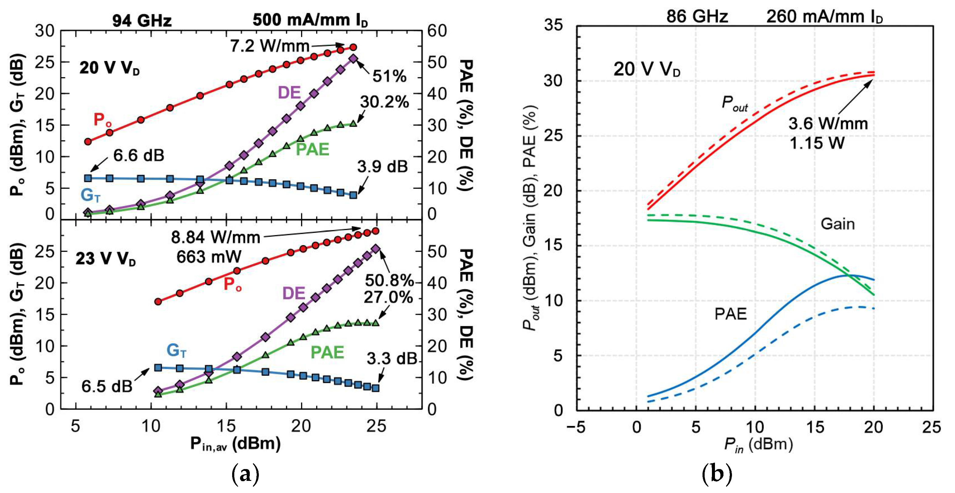
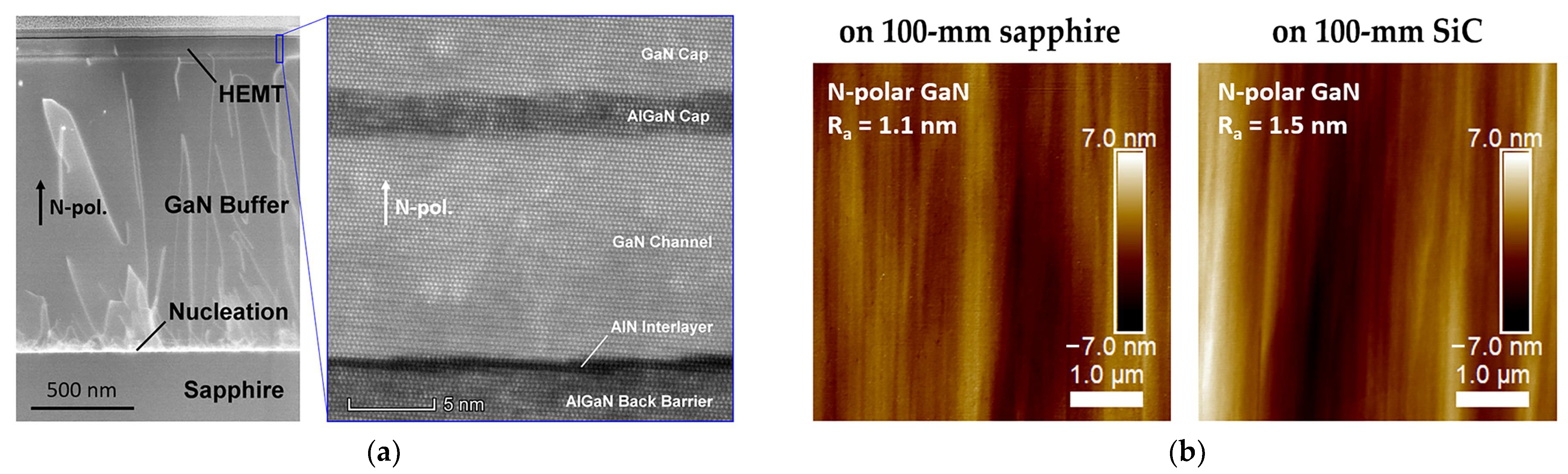
4.2. Research Advances
5. Conclusions
Author Contributions
Funding
Data Availability Statement
Acknowledgments
Conflicts of Interest
References
- Fujita, S. Wide-bandgap semiconductor materials: For their full bloom. Jpn. J. Appl. Phys. 2015, 54, 030101. [Google Scholar] [CrossRef] [Green Version]
- Roccaforte, F.; Fiorenza, P.; Greco, G.; Lo Nigro, R.; Giannazzo, F.; Iucolano, F.; Saggio, M. Emerging trends in wide band gap semiconductors (SiC and GaN) technology for power devices. Microelectron. Eng. 2018, 187–188, 66–77. [Google Scholar] [CrossRef]
- Dubey, S.K.; Mishra, M.; Islam, A. Characterization of AlGaN / GaN based HEMT for low noise and high frequency application. Int. J. Numer. Model. 2022, 35, e2932. [Google Scholar] [CrossRef]
- Chen, S.; Witkowski, L.; Gu, X. (Invited) Important Recent Advancement of GaN Technology and MMICs for W-Band Applications. ECS Trans. 2017, 80, 945–952. [Google Scholar] [CrossRef]
- Ye, R.; Cai, X.; Du, C.; Liu, H.; Zhang, Y.; Duan, X.; Zhu, J. An Overview on Analyses and Suppression Methods of Trapping Effects in AlGaN/GaN HEMTs. IEEE Access 2022, 10, 21759–21773. [Google Scholar] [CrossRef]
- Rongming, C.; Likun, S.; Fichtenbaum, N.; Zhen, C.; Keller, S.; DenBaars, S.P.; Mishra, U.K. Correlation Between DC–RF Dispersion and Gate Leakage in Deeply Recessed GaN/AlGaN/GaN HEMTs. IEEE Electron Device Lett. 2008, 29, 303–305. [Google Scholar] [CrossRef]
- Rawal, D.S.; Amit; Sharma, S.; Kapoor, S.; Laishram, R.; Vinayak, S. Current collapse scaling in GaN/AlGaN/SiC high electron mobility transistors. Solid State Electron. Lett. 2019, 1, 30–37. [Google Scholar] [CrossRef]
- Shuxun, L.; Maoju, W.; Bing, X.; Wen, C.P.; Min, Y.; Jinyan, W.; Yilong, H.; Wengang, W.; Sen, H.; Chen, K.J. Bo Shen Reduction of Current Collapse in GaN High-Electron Mobility Transistors Using a Repeated Ozone Oxidation and Wet Surface Treatment. IEEE Electron Device Lett. 2015, 36, 757–759. [Google Scholar] [CrossRef]
- Madan, J.; Pandey, R.; Arora, H.; Chaujar, R. Analysis of Varied Dielectrics as Surface Passivation on AlGaN/GaN HEMT for Analog Applications. In Proceedings of the 2018 6th Edition of International Conference on Wireless Networks & Embedded Systems (WECON), Rajpura, India, 16–17 November 2018; pp. 15–18. [Google Scholar]
- Hasan, M.T.; Asano, T.; Tokuda, H.; Kuzuhara, M. Current Collapse Suppression by Gate Field-Plate in AlGaN/GaN HEMTs. IEEE Electron Device Lett. 2013, 34, 1379–1381. [Google Scholar] [CrossRef]
- Sarkar, S.; Khade, R.P.; DasGupta, A.; DasGupta, N. Effect of GaN cap layer on the performance of AlInN/GaN-based HEMTs. Microelectron. Eng. 2022, 258, 111756. [Google Scholar] [CrossRef]
- Song, L.; Fu, K.; Zhang, Z.; Sun, S.; Li, W.; Yu, G.; Hao, R.; Fan, Y.; Shi, W.; Cai, Y.; et al. Interface Si donor control to improve dynamic performance of AlGaN/GaN MIS-HEMTs. AIP Adv. 2017, 7, 125023. [Google Scholar] [CrossRef] [Green Version]
- Longobardi, G.; Udrea, F.; Sque, S.; Hurkx, G.A.M.; Croon, J.; Napoli, E.; Sonsky, J. Impact of Donor Traps on the 2DEG and Electrical Behavior of AlGaN/GaN MISFETs. IEEE Electron Device Lett. 2014, 35, 27–29. [Google Scholar] [CrossRef]
- Miczek, M.; Mizue, C.; Hashizume, T.; Adamowicz, B. Effects of interface states and temperature on the C-V behavior of metal/insulator/AlGaN/GaN heterostructure capacitors. J. Appl. Phys. 2008, 103, 104510. [Google Scholar] [CrossRef] [Green Version]
- Green, B.M.; Chu, K.K.; Chumbes, E.M.; Smart, J.A.; Shealy, J.R.; Eastman, L.F. The effect of surface passivation on the microwave characteristics of undoped AlGaN/GaN HEMTs. IEEE Electron Device Lett. 2000, 21, 268–270. [Google Scholar] [CrossRef]
- Jogai, B. Influence of surface states on the two-dimensional electron gas in AlGaN/GaN heterojunction field-effect transistors. J. Appl. Phys. 2003, 93, 1631–1635. [Google Scholar] [CrossRef]
- Ibbetson, J.P.; Fini, P.T.; Ness, K.D.; DenBaars, S.P.; Speck, J.S.; Mishra, U.K. Polarization effects, surface states, and the source of electrons in AlGaN/GaN heterostructure field effect transistors. Appl. Phys. Lett. 2000, 77, 250–252. [Google Scholar] [CrossRef]
- Vetury, R.; Zhang, N.Q.; Keller, S.; Mishra, U.K. The impact of surface states on the DC and RF characteristics of AlGaN/GaN HFETs. IEEE Trans. Electron Devices 2001, 48, 560–566. [Google Scholar] [CrossRef]
- Hwang, I.; Kim, J.; Chong, S.; Choi, H.-S.; Hwang, S.-K.; Oh, J.; Shin, J.K.; Chung, U.-I. Impact of Channel Hot Electrons on Current Collapse in AlGaN/GaN HEMTs. IEEE Electron Device Lett. 2013, 34, 1494–1496. [Google Scholar] [CrossRef]
- Meneghesso, G.; Verzellesi, G.; Pierobon, R.; Rampazzo, F.; Chini, A.; Mishra, U.K.; Canali, C.; Zanoni, E. Surface-Related Drain Current Dispersion Effects in AlGaN–GaN HEMTs. IEEE Trans. Electron Devices 2004, 51, 1554–1561. [Google Scholar] [CrossRef]
- Patanvariya, D.G.; Kumar, S.; Giri, L.I. Influence of Current Collapse in AlGaN/GaN High Electron Mobility Transistors. In Proceedings of the 2019 10th International Conference on Computing, Communication and Networking Technologies (ICCCNT), Kanpur, India, 6–8 July 2019; pp. 1–5. [Google Scholar]
- Huang, H.; Liang, Y.C.; Samudra, G.S.; Chang, T.-F.; Huang, C.-F. Effects of Gate Field Plates on the Surface State Related Current Collapse in AlGaN/GaN HEMTs. IEEE Trans. Power Electron. 2014, 29, 2164–2173. [Google Scholar] [CrossRef]
- Tingting, Y.; Xinyu, L.; Yingkui, Z.; Chengzhan, L.; Ke, W.; Guoguo, L. Impact of UV/ozone surface treatment on AlGaN/GaN HEMTs. J. Semicond. 2009, 30, 124001. [Google Scholar] [CrossRef]
- King, S.W.; Barnak, J.P.; Bremser, M.D.; Tracy, K.M.; Ronning, C.; Davis, R.F.; Nemanich, R.J. Cleaning of AlN and GaN surfaces. J. Appl. Phys. 1998, 84, 5248–5260. [Google Scholar] [CrossRef]
- Diale, M.; Auret, F.D.; van der Berg, N.G.; Odendaal, R.Q.; Roos, W.D. Analysis of GaN cleaning procedures. Appl. Surf. Sci. 2005, 246, 279–289. [Google Scholar] [CrossRef]
- Kim, J.H.; Choi, H.G.; Ha, M.-W.; Song, H.J.; Roh, C.H.; Lee, J.H.; Park, J.H.; Hahn, C.-K. Effects of Nitride-Based Plasma Pretreatment Prior to SiNx Passivation in AlGaN/GaN High-Electron-Mobility Transistors on Silicon Substrates. Jpn. J. Appl. Phys. 2010, 49, 04DF05. [Google Scholar]
- Romero, M.F.; Jimenez, A.; Miguel-Sanchez, J.; Brana, A.F.; Gonzalez-Posada, F.; Cuerdo, R.; Calle, F.; Munoz, E. Effects of N-2 plasma pretreatment on the SiN passivation of AlGaN/GaN HEMT. IEEE Electron Device Lett. 2008, 29, 209–211. [Google Scholar] [CrossRef]
- Shih-Chien, L.; Bo-Yuan, C.; Yueh-Chin, L.; Ting-En, H.; Huan-Chung, W.; Chang, E.Y. GaN MIS-HEMTs With Nitrogen Passivation for Power Device Applications. IEEE Electron Device Lett. 2014, 35, 1001–1003. [Google Scholar] [CrossRef]
- Mi, M.; Lu, Y.; Hao, Y.; Ma, X.; Yang, L.; Hou, B.; Zhang, M. Improved fmax and breakdown voltage in AlGaN/GaN HEMT with plasma treatment. In Proceedings of the 2018 1st Workshop on Wide Bandgap Power Devices and Applications in Asia (WiPDA Asia), Xi’an, China, 16–18 May 2018; pp. 208–211. [Google Scholar]
- Machuca, F.; Liu, Z.; Sun, Y.; Pianetta, P.; Spicer, W.E.; Pease, R.F.W. Simple method for cleaning gallium nitride (0001). J. Vac. Sci. Technol. A Vac. Surf. Film. 2002, 20, 1784–1786. [Google Scholar] [CrossRef]
- Geng, K.; Chen, D.; Zhou, Q.; Wang, H. AlGaN/GaN MIS-HEMT with PECVD SiNx, SiON, SiO2 as Gate Dielectric and Passivation Layer. Electronics 2018, 7, 416. [Google Scholar] [CrossRef] [Green Version]
- Grabow, L.C.; Uhlrich, J.J.; Kuech, T.F.; Mavrikakis, M. Effectiveness of in situ NH3 annealing treatments for the removal of oxygen from GaN surfaces. Surf. Sci. 2009, 603, 387–399. [Google Scholar] [CrossRef]
- Cheng, K.-Y.; Wu, S.-C.; Yu, C.-J.; Wang, T.-W.; Liao, J.-H.; Wu, M.-C. Comparative study on performance of AlGaN/GaN MS-HEMTs with SiNx, SiOx, and SiNO surface passivation. Solid-State Electron. 2020, 170, 107824. [Google Scholar] [CrossRef]
- Huang, T.; Malmros, A.; Bergsten, J.; Gustafsson, S.; Axelsson, O.; Thorsell, M.; Rorsman, N. Suppression of Dispersive Effects in AlGaN/GaN High-Electron-Mobility Transistors Using Bilayer SiNx Grown by Low Pressure Chemical Vapor Deposition. IEEE Electron Device Lett. 2015, 36, 537–539. [Google Scholar] [CrossRef]
- Zhao, S.-X.; Liu, X.-Y.; Zhang, L.-Q.; Huang, H.-F.; Shi, J.-S.; Wang, P.-F. Impacts of Thermal Atomic Layer-Deposited AlN Passivation Layer on GaN-on-Si High Electron Mobility Transistors. Nanoscale Res. Lett. 2016, 11, 137. [Google Scholar] [CrossRef] [PubMed] [Green Version]
- Huang, S.; Jiang, Q.; Yang, S.; Zhou, C.; Chen, K.J. Effective Passivation of AlGaN/GaN HEMTs by ALD-Grown AlN Thin Film. IEEE Electron Device Lett. 2012, 33, 516–518. [Google Scholar] [CrossRef]
- Liu, S.C.; Wong, Y.-Y.; Lin, Y.-C.; Chang, E.Y. Low Current Collapse and Low Leakage GaN MIS-HEMT Using AlN/SiN as Gate Dielectric and Passivation Layer. ECS Trans. 2014, 61, 211–214. [Google Scholar] [CrossRef] [Green Version]
- Huang, T.; Bergsten, J.; Thorsell, M.; Rorsman, N. Small- and Large-Signal Analyses of Different Low-Pressure-Chemical-Vapor-Deposition SiNx Passivations for Microwave GaN HEMTs. IEEE Trans. Electron Devices 2018, 65, 908–914. [Google Scholar] [CrossRef]
- Godfrey, D.; Nirmal, D.; Arivazhagan, L.; Godwinraj, D.; Mohan Kumar, N.; Chen, Y.; Yeh, W. Current collapse degradation in GaN High Electron Mobility Transistor by virtual gate. Microelectron. J. 2021, 118, 105293. [Google Scholar] [CrossRef]
- Arulkumaran, S.; Egawa, T.; Ishikawa, H. Studies on the Influences of i -GaN, n -GaN, p -GaN and InGaN Cap Layers in AlGaN/GaN High-Electron-Mobility Transistors. Jpn. J. Appl. Phys. 2005, 44, 2953–2960. [Google Scholar] [CrossRef]
- Kordoš, P.; Bernát, J.; Marso, M. Impact of layer structure on performance of unpassivated AlGaN/GaN HEMT. Microelectron. J. 2005, 36, 438–441. [Google Scholar] [CrossRef]
- Mitrofanov, O.; Manfra, M.; Weimann, N. Impact of Si doping on radio frequency dispersion in unpassivated GaN/AlGaN/GaN high-electron-mobility transistors grown by plasma-assisted molecular-beam epitaxy. Appl. Phys. Lett. 2003, 82, 4361–4363. [Google Scholar] [CrossRef] [Green Version]
- Gambin, V.; Gu, X.; Heying, B. AIN buffer N-polar GaN HEMT Profile. Patent US8710511B2, 4 April 2014. [Google Scholar]
- Gambin, V.; GU, X. Ingan channel n-polar gan hemt Profile. Patent WO2014031229A1, 27 February 2014. [Google Scholar]
- Wong, M.H.; Keller, S.; Nidhi, S.D.; Denninghoff, D.J.; Kolluri, S.; Brown, D.F.; Lu, J.; Fichtenbaum, N.A.; Ahmadi, E.; Singisetti, U.; et al. N-polar GaN epitaxy and high electron mobility transistors. Semicond. Sci. Technol. 2013, 28, 074009. [Google Scholar] [CrossRef] [Green Version]
- Nakajima, A.; Fujii, K.; Horio, K. Numerical Analysis of Buffer-Trap Effects on Gate Lag in AlGaN/GaN High Electron Mobility Transistors. Jpn. J. Appl. Phys. 2011, 50, 104303. [Google Scholar] [CrossRef]
- Smorchkova, I.; Grundbacher, R.; Gambin, V.; Gu, X.; Lewis, G.; Oshita, F.; Namba, C.; Liu, P.; Poust, S.; Nam, P.; et al. N-Face GaN HEMT Technology for Next-Generation Mixed-Signal Electronics. In Proceedings of the 37th Annual GOMACTech Conference, Las Vegas, NV, USA, 19–22 March 2012. [Google Scholar]
- Gu, X.; Xie, J.; Lee, C. Process of fabricating high efficiency, high linearity N-polar gallium-nitride (GaN) Transistors. Patent US10749009B1, 18 August 2020. [Google Scholar]
- Steven, W.; Romanczyk, B.; Guidry, M.; Li, H.; Ahmadi, E.; Hestroffer, K.; Zheng, X.; Keller, S.; Mishra, U.K. N-Polar GaN Cap MISHEMT With Record Power Density Exceeding 6.5 W/mm at 94 GHz. IEEE Electron Device Lett. 2017, 38, 359–362. [Google Scholar]
- Shen, L.; Coffie, R.; Buttari, D.; Heikman, S.; Chakraborty, A.; Chini, A.; Keller, S.; DenBaars, S.P.; Mishra, U.K. High-Power Polarization-Engineered GaN/AlGaN/GaN HEMTs Without Surface Passivation. IEEE Electron Device Lett. 2004, 25, 7–9. [Google Scholar] [CrossRef]
- Shen, L.; Palacios, T.; Poblenz, C.; Corrion, A.; Chakraborty, A.; Fichtenbaum, N.; Keller, S.; Denbaars, S.P.; Speck, J.S.; Mishra, U.K. Unpassivated high power deeply recessed GaN HEMTs with fluorine-plasma surface treatment. IEEE Electron Device Lett. 2006, 27, 214–216. [Google Scholar] [CrossRef] [Green Version]
- Shen, L.; Pei, Y.; McCarthy, L.; Poblenz, C.; Corrion, A.; Fichtenbaum, N.; Keller, S.; Denbaars, S.P.; Speck, J.S.; Mishra, U.K. Deep-recessed GaN HEMTs using selective etch technology exhibiting high microwave performance without surface passivation. In Proceedings of the 2007 IEEE/MTT-S International Microwave Symposium, Honolulu, HI, USA, 3–8 June 2007; pp. 623–626. [Google Scholar]
- Romanczyk, B.; Wienecke, S.; Guidry, M.; Li, H.; Ahmadi, E.; Zheng, X.; Keller, S.; Mishra, U.K. Demonstration of Constant 8 W/mm Power Density at 10, 30, and 94 GHz in State-of-the-Art Millimeter-Wave N-Polar GaN MISHEMTs. IEEE Trans. Electron Devices 2018, 65, 45–50. [Google Scholar] [CrossRef]
- Kolluri, S.; Brown, D.F.; Wong, M.H.; Dasgupta, S.; Keller, S.; DenBaars, S.P.; Mishra, U.K. RF Performance of Deep-Recessed N-Polar GaN MIS-HEMTs Using a Selective Etch Technology Without Ex Situ Surface Passivation. IEEE Electron Device Lett. 2011, 32, 134–136. [Google Scholar] [CrossRef]
- Wienecke, S.; Romanczyk, B.; Guidry, M.; Li, H.; Zheng, X.; Ahmadi, E.; Hestroffer, K.; Megalini, L.; Keller, S.; Mishra, U.K. N-Polar Deep Recess MISHEMTs with Record 2.9 W/mm at 94 GHz. IEEE Electron Device Lett. 2016, 37, 713–716. [Google Scholar] [CrossRef]
- Mohapatra, M.; De, T.; Panda, A.K. Performance analysis of AlGaN/GaN based HEMT for different gate structure (Normal gate and T-shaped gate). In Proceedings of the 2017 Devices for Integrated Circuit (DevIC), Kalyani, India, 23–24 March 2017; pp. 144–148. [Google Scholar]
- Zheng, X.; Guidry, M.; Li, H.; Romanczyk, B.; Ahmadi, E.; Hestroffer, K.; Wienecke, S.; Keller, S.; Mishra, U.K. N-polar GaN MIS-HEMTs on sapphire with a proposed figure of merit fmax·VDS, Q of 9.5 THz.V. In Proceedings of the 2017 75th Annual Device Research Conference (DRC), South Bend, IN, USA, 25–28 June 2017; pp. 1–2. [Google Scholar]
- Zheng, X.; Li, H.; Ahmadi, E.; Hestroffer, K.; Guidry, M.; Romanczyk, B.; Wienecke, S.; Keller, S.; Mishra, U.K. High frequency N-polar GaN planar MIS-HEMTs on sapphire with high breakdown and low dispersion. In Proceedings of the 2016 Lester Eastman Conference (LEC), Bethlehem, PA, USA, 2–4 August 2016; pp. 42–45. [Google Scholar]
- Wienecke, S.M. N-Polar Deep Recess MISHEMTs for mm-Wave Applications. Ph.D. Thesis, University of California-Santa Barbara, Los Angeles, CA, USA, 2018. [Google Scholar]
- Romanczyk, B.; Wienecke, S.; Guidry, M.; Li, H.; Hestroffer, K.; Ahmadi, E.; Zheng, X.; Keller, S.; Mishra, U.K. mm-Wave N-polar GaN MISHEMT with a self-aligned recessed gate exhibiting record 4.2 W/mm at 94 GHz on Sapphire. In Proceedings of the 2016 74th Annual Device Research Conference (DRC), Newark, DE, USA, 19–22 June 2016; pp. 1–2. [Google Scholar]
- Romanczyk, B.; Li, W.; Guidry, M.; Hatui, N.; Krishna, A.; Wurm, C.; Keller, S.; Mishra, U.K. N-Polar GaN-on-Sapphire Deep Recess HEMTs With High W-Band Power Density. IEEE Electron Device Lett. 2020, 41, 1633–1636. [Google Scholar] [CrossRef]
- Romanczyk, B.; Zheng, X.; Guidry, M.; Li, H.; Hatui, N.; Wurm, C.; Krishna, A.; Ahmadi, E.; Keller, S.; Mishra, U.K. W-Band Power Performance of SiN-Passivated N-Polar GaN Deep Recess HEMTs. IEEE Electron Device Lett. 2020, 41, 349–352. [Google Scholar] [CrossRef]
- Romanczyk, B.; Guidry, M.; Zheng, X.; Shrestha, P.; Li, H.; Ahmadi, E.; Keller, S.; Mishra, U.K. Evaluation of linearity at 30 GHz for N-polar GaN deep recess transistors with 10.3 W/mm of output power and 47.4% PAE. Appl. Phys. Lett. 2021, 119, 072105. [Google Scholar] [CrossRef]
- Niida, Y.; Kamada, Y.; Ohki, T.; Ozaki, S.; Makiyama, K.; Minoura, Y.; Okamoto, N.; Sato, M.; Joshin, K.; Watanabe, K. 3.6 W/mm high power density W-band InAlGaN/GaN HEMT MMIC power amplifier. In Proceedings of the 2016 IEEE Topical Conference on Power Amplifiers for Wireless and Radio Applications (PAWR), Austin, TX, USA, 24–27 January 2016; pp. 24–26. [Google Scholar]
- Harrouche, K.; Kabouche, R.; Okada, E.; Medjdoub, F. High Performance and Highly Robust AlN/GaN HEMTs for Millimeter-Wave Operation. IEEE J. Electron Devices Soc. 2019, 7, 1145–1150. [Google Scholar] [CrossRef]
- Shrestha, P.; Guidry, M.; Romanczyk, B.; Hatui, N.; Wurm, C.; Krishna, A.; Pasayat, S.S.; Karnaty, R.R.; Keller, S.; Buckwalter, J.F.; et al. High Linearity and High Gain Performance of N-Polar GaN MIS-HEMT at 30 GHz. IEEE Electron Device Lett. 2020, 41, 681–684. [Google Scholar] [CrossRef]
- Bisi, D.; Romanczyk, B.; Liu, X.; Gupta, G.; Brown-Heft, T.; Birkhahn, R.; Lal, R.; Neufeld, C.J.; Keller, S.; Parikh, P.; et al. Commercially Available N-polar GaN HEMT Epitaxy for RF Applications. In Proceedings of the 2021 IEEE 8th Workshop on Wide Bandgap Power Devices and Applications (WiPDA), Redondo Beach, CA, USA, 7–9 November 2021; pp. 250–254. [Google Scholar]
- Gu, X.; Lee, C.; Xie, J.; Beam, E.; Becker, M.; Grotjohn, T.; Anaya, J.; Kuball, M. GaN-on-Diamond with Ultra-Low Thermal Barrier Resistance; Qorvo Inc.: Richardson, TX, USA, 2016. [Google Scholar]
- Zhou, Y.; Anaya, J.; Pomeroy, J.; Sun, H.; Gu, X.; Xie, A.; Beam, E.; Becker, M.; Grotjohn, T.A.; Lee, C.; et al. Barrier-Layer Optimization for Enhanced GaN-on-Diamond Device Cooling. ACS Appl. Mater. Interfaces 2017, 9, 34416–34422. [Google Scholar] [CrossRef] [PubMed]
- Yates, L.; Anderson, J.; Gu, X.; Lee, C.; Bai, T.; Mecklenburg, M.; Aoki, T.; Goorsky, M.S.; Kuball, M.; Piner, E.L.; et al. Low Thermal Boundary Resistance Interfaces for GaN-on-Diamond Devices. ACS Appl. Mater. Interfaces 2018, 10, 24302–24309. [Google Scholar] [CrossRef] [PubMed]
- Romanczyk, B.; Guidry, M.; Wienecke, S.; Li, H.; Ahmadi, E.; Zheng, X.; Keller, S.; Mishra, U.K. W-band N-polar GaN MISHEMTs with high power and record 27.8% efficiency at 94 GHz. In Proceedings of the 2016 IEEE International Electron Devices Meeting (IEDM), San Francisco, CA, USA, 3–7 December 2016; pp. 3.5.1–3.5.4. [Google Scholar]
- Liu, W.; Romanczyk, B.; Guidry, M.; Hatui, N.; Wurm, C.; Li, W.; Shrestha, P.; Zheng, X.; Keller, S.; Mishra, U.K. 6.2 W/Mm and Record 33.8% PAE at 94 GHz From N-Polar GaN Deep Recess MIS-HEMTs With ALD Ru Gates. IEEE Microw. Wirel. Compon. Lett. 2021, 31, 748–751. [Google Scholar] [CrossRef]
- Romanczyk, B.; Guidry, M.; Zheng, X.; Li, H.; Ahmadi, E.; Keller, S.; Mishra, U.K. Bias-Dependent Electron Velocity Extracted From N-Polar GaN Deep Recess HEMTs. IEEE Trans. Electron Devices 2020, 67, 1542–1546. [Google Scholar] [CrossRef]
- Romanczyk, B.; Guidry, M.; Wienecke, S.; Li, H.; Ahmadi, E.; Zheng, X.; Keller, S.; Mishra, U.K. Record 34.2% efficient mm-wave N-polar AlGaN/GaN MISHEMT at 87 GHz. Electron. Lett. 2016, 52, 1813–1814. [Google Scholar] [CrossRef]


| Type | Empty | Filled |
|---|---|---|
| Donor surface states | Positive | Neutral |
| Acceptor surface states | Neutral | Negative |
| Ref. | Band | Freq. (GHz) | Peak Po | Peak PAE | Disp. (%) | Cap Thk. (nm) | SiNx Thk. (nm) | Substrate | ||||
|---|---|---|---|---|---|---|---|---|---|---|---|---|
| VD(V) | Po (W/mm) | PAE (%) | VD(V) | Po (W/mm) | PAE (%) | |||||||
| [55] | W | 94 | 10 | 2.9 | 15.5 | 8 | 1.7 | 20 | 110 | 18 | Sapphire | |
| [60] | 14 | 4.2 | 8 | 1.6 | 16.5 | 22 | NO | Sapphire | ||||
| [61] | 16 | 5.5 | 20.6 | 12 | 3.7 | 25.9 | <5 | 20 | 20 | Sapphire | ||
| [71] | 11 | 3.7 | 9 | 3.0 | 27.8 | <5 | 47.5 | NO | SiC | |||
| [72] | 18 | 6.2 | 33.8 | 16 | 5.6 | 34.8 | 47.5 | 24 | SiC | |||
| [49] | 16 | 6.7 | 14.4 | 15 | 4.8 | 16.9 | NO | 47.5 | NO | SiC | ||
| [73] | 20 | 7.1 | 25.1 | 14 | 4.6 | 27.5 | 47.5 | NO | SiC | |||
| [53] | 20 | 7.9 | 26.9 | 16 | 5.3 | 28.8 | <10 | 47.5 | NO | SiC | ||
| [62] | 23 | 8.8 | 27 | 20 | 7.2 | 30.2 | 8.5 | 47.5 | 40 | SiC | ||
| [74] | 87 | 8 | 2.5 | 34.2 | NO | 47.5 | NO | SiC | ||||
| [66] | Ka | 30 | 10 | 12.6 | 20 | SiC | ||||||
| [53] | 20 | 8.1 | 52.5 | 14 | 5.6 | 55.9 | <10 | 47.5 | NO | SiC | ||
| [63] | 26 | 10.3 | 47.4 | 47.5 | 40 | SiC | ||||||
| [53] | X | 10 | 20 | 7.8 | 54.9 | 14 | 5.1 | 58.1 | <10 | 47.5 | NO | SiC |
| [54] | C | 4 | 24 | 5.5 | 74 | NO | 120 | NO | Sapphire | |||
Publisher’s Note: MDPI stays neutral with regard to jurisdictional claims in published maps and institutional affiliations. |
© 2022 by the authors. Licensee MDPI, Basel, Switzerland. This article is an open access article distributed under the terms and conditions of the Creative Commons Attribution (CC BY) license (https://creativecommons.org/licenses/by/4.0/).
Share and Cite
Zhu, P.; Ni, X.; Fan, Q.; Gu, X. Surface Dispersion Suppression in High-Frequency GaN Devices. Crystals 2022, 12, 1461. https://doi.org/10.3390/cryst12101461
Zhu P, Ni X, Fan Q, Gu X. Surface Dispersion Suppression in High-Frequency GaN Devices. Crystals. 2022; 12(10):1461. https://doi.org/10.3390/cryst12101461
Chicago/Turabian StyleZhu, Pengfei, Xianfeng Ni, Qian Fan, and Xing Gu. 2022. "Surface Dispersion Suppression in High-Frequency GaN Devices" Crystals 12, no. 10: 1461. https://doi.org/10.3390/cryst12101461