Article

Effect of Source Field Plate Cracks on the Electrical Performance of AlGaN/GaN HEMT Devices

1
State Key Laboratory of Mobile Network and Mobile Multimedia Technology, Shenzhen 518055, China
2
Wireless Product Planning Department, ZTE Corporation, Shenzhen 518057, China
3
School of Microelectronics, Xidian University, Xi’an 710071, China
*
Authors to whom correspondence should be addressed.
Crystals 2022, 12(9), 1195; https://doi.org/10.3390/cryst12091195
Submission received: 29 July 2022 / Revised: 22 August 2022 / Accepted: 23 August 2022 / Published: 25 August 2022
(This article belongs to the Special Issue Recent Advances in III-Nitride Semiconductors)

Abstract

:
In the current study, the effects of cracks in source field plates (SFPs) on the electrical performance of AlGaN/GaN high electron mobility transistors (HEMTs) are investigated systematically using numerical simulation. In detail, the influence of crack width and junction angle in SFPs on device performance is studied. The results indicate that the SFP structure increases the breakdown voltage of a device, but the occurrence of cracks causes premature breakdown, which is confirmed experimentally by the structural analysis of these devices after breakdown. With an increase in crack width, the electrical performance becomes worse. A beveled SFP architecture is proposed by increasing the angle at the SFP junction to reduce the probability of cracking and enhance the reliability of the device. However, with an increase in bevel angle, the modulation effect of the SFP on the channel electric field is gradually weakened. Therefore, it is necessary to balance the relationship between electrical performance and bevel angle according to the actual demands. This work provides potential support for SFP structural optimization design for AlGaN/GaN HEMTs.

1. Introduction

Compared with silicon, gallium nitride (GaN) has a wider band gap, higher thermal conductivity and higher electron mobility in AlGaN/GaN heterostructures. At present, GaN-based power and radio frequency high-electron-mobility transistors (HEMTs) show excellent performance and are widely applied in the field of base station communication, aerospace and radar systems [1,2,3,4]. As a core component of the power amplifier (PA) in the radio remote unit of a base station, the failure of an AlGaN/GaN HEMT reduces the product yield, work efficiency and service life, further aggravating the failure rate of PAs.
AlGaN/GaN HEMTs usually work under high-frequency and high-voltage conditions. On the one hand, low-frequency dispersion is induced by traps and has an impact on high-frequency performance [5,6,7]. On the other hand, these devices need to withstand extremely high drain voltages. The electric potential lines gather at either the gate or drain of the device and result in an electric field peak. When the electric field peak is higher than the critical breakdown electric field, avalanche ionization occurs and the device breaks down [8,9]. Therefore, it is necessary to optimize the electric field distribution by designing the device structure so as to improve the breakdown voltage (Vbr). The electrical characteristics of AlGaN/GaN HEMTs can be enhanced by introducing a field plate structure, which brings in a uniform space charge distribution in a lateral direction and, therefore, increases the Vbr [10,11,12,13,14,15]. In a failure analysis and reliability study of AlGaN/GaN HEMTs, cracks are always found at the junctions of the source field plate (SFP). It is reported that these cracks may come from the process of field plate metal deposition on uneven surfaces because of the stresses at these junctions [16,17,18]. However, SFP cracks are potentially risky, and their effects on a device’s electrical performance are still unclear; therefore, further research is urgently needed.
In this work, firstly, an AlGaN/GaN HEMT device with an SFP structure is characterized experimentally after its breakdown, and cracks are found at the junctions of the SFP. Secondly, the effects of these SFP cracks on the device’s electrical performance are studied systematically based on TCAD simulations. Various device structures with and without an SFP and with differing crack widths are simulated and compared. Finally, a beveled SFP architecture is proposed to provide a feasible solution for avoiding cracks and increasing the reliability of AlGaN/GaN HEMTs.

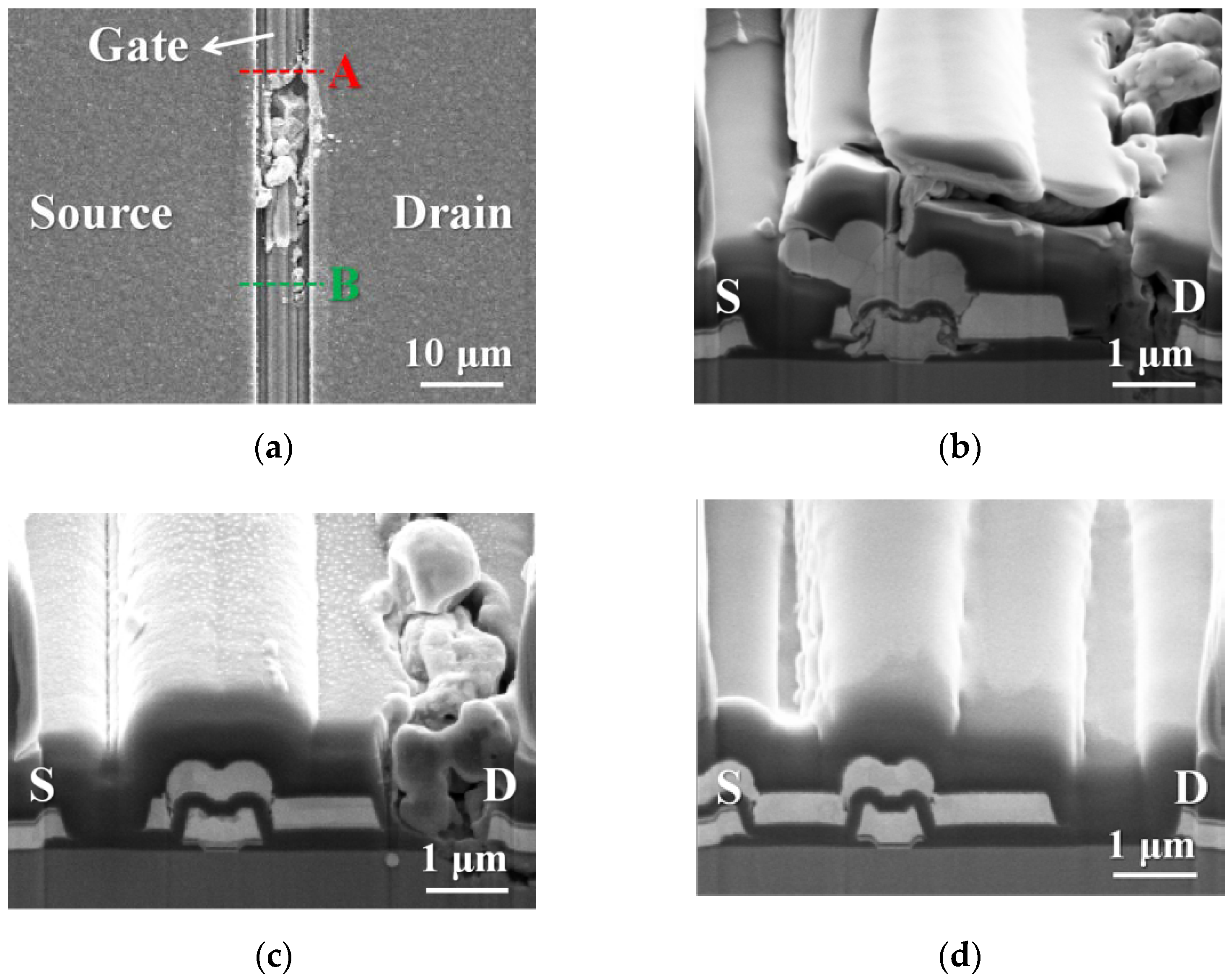
2. Failure Analysis Experiments

During the failure analysis of a commercial AlGaN/GaN HEMT device, a large number of focused ion beam (FIB, Thermo Scientific Helios G4 PFIB UXe DualBeam system) characterizations were carried out after breakdown. The images were acquired at 5 kV and 0.17 nA under secondary electron imaging mode. From scanning electron microscope (SEM) surface morphology, the gate metal at the breakdown points was broken or partially damaged, as shown in Figure 1a. FIB cross-section characterization was carried out at position A, near the breakdown point as shown in Figure 1b. The morphology of the gate metal was partially damaged, and there was a crack in the SFP near the drain side. The SFP broke at the crack and was lifted near the source side. Position B, with a better surface morphology below the breakdown point, was characterized as shown in Figure 1c. The SFP was disconnected, and there were cracks at the junctions above the gate cap. Another position, C (not shown in Figure 1a), on the same gate where no breakdown occurred was also characterized. As shown in Figure 1d, the SFP was still connected, but there was also a trend of cracking at the junctions. It is inferred that the cracks were not caused by breakdown but caused by the SFP deposition process, since there was no crack in the secondary passivation layer between the SFP and the gate cap. In the SFP deposition process, the metal is relatively prone to fracture due to stress [16,17,18]. According to the FIB characterization results, there is a certain correlation between gate breakdown and SFP cracking; however, a further study of the internal mechanism is still needed.

3. Materials and Methods

APSYS (Crosslight, Vancouver, Canada) device simulations were carried out to analyze the detailed electrical characteristics [19]. The simulated AlGaN/GaN HEMT structure with a T-gate is illustrated in Figure 2. The epitaxial layer structure consisted of an n-doped (2 × 1016 cm−3) semi-insulating SiC substrate layer, AlN nucleation layer, GaN buffer layer and GaN channel layer. Above these were an unintentionally doped Al0.3Ga0.7N barrier layer and a SiN passivation layer. Traps with a maximum concentration of 1 × 1017 cm−3 and a relative energy level of 0.45 eV were assigned to model Fe doping in the buffer layer [20,21]. Two-dimensional electron gas was generated using interface and polarization statements, and the electron mobility of 1400 cm2V−1s1 was used in the simulation. In order to simulate the breakdown mechanism, the Chenoweth law for impact ionization with user-definable parameters was used [22]. The Vbr was defined as the drain voltage when the drain-to-source current reached 1 mA/mm [10,23].
A Schottky contact with a work function of 5.4 eV was used as a gate electrode, and an ohmic contact with a work function of 4.0 eV was used for the source and drain electrodes. For the AlGaN/GaN HEMT with a cracked SFP, the crack height was set as 200 nm, and the width was varied from 0–50 nm in 10 nm step. In addition, the material within the crack was set as air in the simulation. The SiC substrate and source electrode were grounded. For the breakdown simulation, a gate voltage of Vg = −6 V was applied to imitate the off-state situation. The SFP and source electrode maintained the same potential in the simulation. The other main dimension parameters used are provided in Table 1.

4. Results and Discussion

Cracks of different shapes often appear at the junctions of a SFPs, and it is necessary to investigate the effect of different crack widths on a device’s electrical performance. Therefore, simulations of different AlGaN/GaN HEMT structures were carried out. When w = 0 nm, it means an HEMT with a conventional SFP but without a crack. For comparison, an HEMT without an SFP was also investigated. The transfer and transconductance characteristics of these devices are shown in Figure 3a. The drain voltage (Vd) was set to 10 V, and the gate voltage (Vg) was swept from −6 V–2 V. Then, the threshold voltage (Vth) was extracted from a linear extrapolation of the transfer characteristics at the point of maximum transconductance. The presence of an SFP and SFP cracks had little effect on the transfer and transconductance properties of the device. The Vth and the maximum transconductance were about −2.53 V and 227 mS/mm, respectively. As shown in Figure 3b, the Vbr was 160 V at Vg = −6 V for the HEMT without an SFP. For the HEMT with an SFP, when w increased from 0 nm to 50 nm, the Vbr decreased from 261 V to 181 V. This decreasing trend slowed down when w increased to 20 nm. It was seen that the SFP had a positive effect, improving the Vbr. However, once the SFP had a crack, the Vbr considerably decreased. Furthermore, the relationship between Vbr and Vth depending on crack width is depicted in Figure 3c. Figure 3d shows simulated pulsed I-V characteristics with a 1 μs pulse width and a 1 ms pulse period. The quiescent bias point was set as (Vg,q = −6 V, Vd,q = 80 V). In contrast to the static results, the HEMT with a conventional SFP showed a maximum saturated drain current, while the HEMT without an SFP showed a minimum one. The reason for the discrepancy between the dynamic and static I-V characteristics is that the SFP alleviates the high electric field and restrains the trapping in the buffer [24,25]. The appearance of a crack affected the modulation effect of the SFP on the electric field. As a result, the trapping process increased, and the saturated drain current decreased.
In order to find the weak point where the device is prone to breakdown, the impact ionization rates were simulated at their respective Vbr points. Cross-sections of the impact ionization rate distribution for three different AlGaN/GaN HEMT structures are shown in Figure 4. For the HEMT without an SFP and the HEMT with a 20 nm wide cracked SFP, the max impact ionization rate was located at the gate edge of the drain side. However, if there was no crack in the SFP (w = 0 nm), the position of the max impact ionization rate moved to the SFP edge of the drain side, as shown in Figure 4b. High impact ionization rates lead to enhanced carrier generation and early breakdowns of a device [8,9], and the appearance of an SFP decreases the impact ionization rate and changes the distributions at the same time [13,14].
The potential distributions for the three different aforementioned AlGaN/GaN HEMT structures were simulated at Vg = −6 V and Vd = 160 V. The contours for a closeup region, including the gate and SFP, are shown in Figure 5. It was observed that for the HEMT without an SFP, most of the potential lines crowded at the drain side of the gate, as well as in the barrier and buffer layers. Crowded potential lines usually lead to a high electric field and consequently a high impact ionization rate. For the HEMT with a conventional SFP, high potential line density appeared at both the drain side of the gate and the drain side of the SFP, which is attributed to the modulation effect of the SFP [12,26,27]. The potential line densities in the barrier and buffer layers were also lower than those for the HEMT without an SFP. Once the SFP had cracked, some potential lines appeared in the cracked region. The right part of the SFP did not share the same potential as the left part anymore, and its modulation effect finally weakened.
The electric field is also an important parameter which determines the Vbr of an HEMT device [28,29,30]. Therefore, the electric field along the channel before breakdown (Vg = −6 V, Vd = 160 V) is shown in Figure 6. It was found that the electric field peaks all appeared at the gate edge of the drain side. The HEMT without an SFP showed the maximum electric field peak of 1.82 MV/cm. As the w increased, the electric field peak increased from 1.38 MV/cm to 1.70 MV/cm. It is obvious that the Vbr is inversely proportional to the electric field peak. The field plate plays a major role in the electric field, impact ionization rate distribution and the breakdown of the AlGaN/GaN HEMT; however, the occurrence of a crack will reduce the electric field peak inhibition by the field plate. Given this, the wider the SFP crack becomes, the poorer the electrical performance.
As discussed above, the appearance of SFP cracks degrades the electrical performance of AlGaN/GaN HEMTs. In the process of SFP metal deposition, cracks form easily at these junctions due to the steep angle and high stresses [16,17,18]. High stress usually appears at the right-angled corner. When the angle increases, the stress reduces, and, consequently, the cracking tendency decreases [31,32]. Accordingly, we propose a beveled SFP structure (see Figure 7a) since increasing the bevel angle at this junction may relieve the stress and reduce the probability of cracking. A further simulation study investigating whether the rise of junction angle affects the electrical performance of a device was carried out. For convenience, the angle is named θ as illustrated in Figure 7a. When θ = 90°, it means the HEMT with a conventional SFP of which the junction is a right angle. In the following simulations, the total length of SFP was kept unchanged and θ changed from 90° to 162° (90°, 108°, 135°, 149°, 157° and 162°). The same electrical parameter simulations were carried out as in the above study. As an example, a proposed HEMT with an SFP bevel angle of 108° achieved a Vbr of 256 V, which is very close to the HEMT with a conventional SFP. The channel electric field and the cross-sectional impact ionization rate distributions also showed similar results. As shown in Figure 7b, when θ increased from 90° to 162°, the Vbr decreased from 261 V to 201 V. Furthermore, when θ was increased to 135°, the rate of decline in Vbr increased. Even so, the Vbr of 201 V was still higher than that of the HEMT with a 20 nm wide cracked SFP. The channel electric field peak was extracted before breakdown (Vg = −6 V, Vd = 200 V), and it showed an inverse trend compared with the Vbr. With an increase in θ, the distance from the lower edge of the SFP to the channel becomes longer, so the modulation effect of the SFP on the electric field is weakened [12,33,34]. As a result, the beveled SFP reduces the stress and the risk of cracking, but it also reduces the electrical performance of the device.

5. Conclusions

To investigate the effects of cracks in SFPs on a device’s electrical performance, AlGaN/GaN HEMTs with different SFP structures were studied by using simulations. The results show that compared with the HEMT without an SFP, the HEMT with a conventional SFP showed better breakdown and dynamic I-V performances. However, we found that once a crack appeared in the SFP, the device’s electrical performance degraded, and the decreasing trend slowed down when the crack width increased to 20 nm. The physical mechanism was investigated from the aspects of impact ionization rate, potential and channel electric field. The SFP structure effectively alleviated the peak electric field at the gate edge of the drain side, but the crack reduced the effect of SFP undesirably. The beveled SFP structure is a good strategy to reduce the risk of cracking; however, this is at the expense of a device’s electrical indicators. When the bevel angle increases to 135°, the breakdown voltage begins to drop rapidly. Thus, it is recommended to balance these factors according to actual needs, and a bevel angle of no more than 135° is suggested. Field plate technology is simple and compatible with other electric field optimization technologies. These results can be used for fabricating future HEMT devices with SFPs to achieve a high breakdown voltage and high reliability.

Author Contributions

Conceptualization, Y.-N.B., C.-L.D. and X.-L.C.; characterization, C.-L.D.; simulation, Y.-N.B. and C.-L.D.; data curation and analysis, Y.-N.B., C.-L.D., X.-L.C. and R.Y.; writing—original draft preparation, Y.-N.B. and C.-L.D.; writing—review and editing, Y.-N.B., C.-L.D., X.-L.C., R.Y., H.-J.L., Y.Z., X.-Y.D. and J.-J.Z. All authors have read and agreed to the published version of the manuscript.

Funding

This research was funded by the Fundamental Research Funds for the Central Universities under Grant QTZX22022.

Institutional Review Board Statement

Not applicable.

Informed Consent Statement

Not applicable.

Data Availability Statement

Not applicable.

Conflicts of Interest

The authors declare no conflict of interest.

References

  1. Fletcher, A.S.; Nirmal, D. A survey of gallium nitride HEMT for RF and high power application. J. Superlattice Microst. 2017, 109, 519–537. [Google Scholar] [CrossRef]
  2. Amano, H.; Baines, Y.; Beam, E.; Matteo, B. The 2018 GaN power electronics roadmap. J. Appl. Phys. 2018, 51, 163001. [Google Scholar] [CrossRef]
  3. Nakajima, S. GaN HEMTs for 5G Base Station Applications. In Proceedings of the 2018 IEEE International Electron Devices Meeting (IEDM), San Francisco, CA, USA, 1–5 December 2018; pp. 14.2.1–14.2.4. [Google Scholar]
  4. Huang, L.H.; Chiou, H.K. An Ultra-compact 14.9-W X-Band GaN MMIC Power Amplifier. In Proceedings of the 2020 IEEE Asia-Pacific Microwave Conference (APMC), Hong Kong, China, 8–11 December 2020; pp. 257–259. [Google Scholar]
  5. Jardel, O.; Groote, F.D.; Reveyrand, T.; Jacquet, J.-C.; Charbonniaud, C.; Teyssier, J.-P.; Floriot, D.; Quere, R. An Electrothermal Model for AlGaN/GaN Power HEMTs Including Trapping Effects to Improve Large-Signal Simulation Results on High VSWR. IEEE Trans. Microw. Theory Tech. 2007, 55, 2660–2669. [Google Scholar] [CrossRef]
  6. Raffo, A.; Vadala, V.; Schreurs, D.M.M.-P.; Crupi, G.; Avolio, G.; Caddemi, A.; Vannini, G. Nonlinear Dispersive Modeling of Electron Devices Oriented to GaN Power Amplifier Design. IEEE Trans. Microw. Theory Tech. 2010, 58, 710–718. [Google Scholar] [CrossRef]
  7. Potier, C.; Martin, A.; Campovecchio, M.; Laurent, S.; Quere, R.; Jacquet, J.C.; Jardel, O.; Piotrowicz, S.; Delage, S. Trap characterization of microwave GaN HEMTs based on frequency dispersion of the output-admittance. In Proceedings of the 2014 9th European Microwave Integrated Circuit Conference, Rome, Italy, 6–7 October 2014; pp. 464–467. [Google Scholar]
  8. Gaudenzio, M.; Matteo, M.; Enrico, Z. Breakdown mechanisms in AlGaN/GaN HEMTs: An overview. Jpn. J. Appl. Phys. 2014, 53, 100211. [Google Scholar]
  9. Saito, W.; Suwa, T.; Uchihara, T.; Naka, T.; Kobayashi, T. Breakdown behaviour of high-voltage GaN-HEMTs. Microelectron. Reliab. 2015, 55, 1682–1686. [Google Scholar] [CrossRef]
  10. Kwak, H.T.; Chang, S.B.; Jung, H.G.; Kim, H.S. Thermal Analysis of AlGaN/GaN High-Electron-Mobility Transistor and Its RF Power Efficiency Optimization with Source-Bridged Field-Plate Structure. J. Nanosci. Nanotechnol. 2018, 18, 5860–5867. [Google Scholar] [CrossRef]
  11. Godfrey, D.; Nirmal, D.; Arivazhagan, L.; Roy, B.; Chen, Y.L.; Yu, T.H.; Roy, B.; Yeh, W.K.; Godwinraj, D. Investigation of AlGaN/GaN HEMT Breakdown analysis with Source field plate length for High power applications. In Proceedings of the 2020 5th International Conference on Devices, Circuits and Systems (ICDCS), Coimbatore, India, 5–6 March 2020; pp. 244–246. [Google Scholar]
  12. Liao, B.Y.; Zhou, Q.B.; Qin, J.; Wang, H. Simulation of AlGaN/GaN HEMTs’ Breakdown Voltage Enhancement Using Gate Field-Plate, Source Field-Plate and Drain Field Plate. Electronics 2019, 8, 406. [Google Scholar] [CrossRef]
  13. Soni, A.; Singh, A.; Shrivastava, M. Novel Drain-Connected Field Plate GaN HEMT Designs for Improved VBD–RON Tradeoff and RF PA Performance. IEEE Trans. Electron Devices 2020, 67, 1718–1725. [Google Scholar] [CrossRef]
  14. Augustine Fletcher, A.S.; Nirmal, D.; Ajayan, J.; Arivazhagan, L. Analysis of AlGaN/GaN HEMT using discrete field plate technique for high power and high frequency applications. AEU Int. J. Electron. Commun. 2019, 99, 325–330. [Google Scholar] [CrossRef]
  15. Kwak, H.K.; Jang, K.W.; Kim, H.J.; Lee, S.H.; Lim, J.W.; Kim, H.S. DC Characteristics of AlGaN/GaN High-Electron Mobility Transistor with a Bottom Plate Connected to Source-Bridged Field Plate Structure. J. Nanosci. Nanotechnol. 2019, 19, 2319–2322. [Google Scholar] [CrossRef] [PubMed]
  16. Zhou, L.; San, Z.W.; Hua, Y.J.; Lin, L.; Zhang, S.; Zhao, Z.G.; Zhou, H.J.; Yin, W.Y. Investigation on Failure Mechanisms of GaN HEMT Caused by High-Power Microwave (HPM) Pulses. IEEE Trans. Electromagn. Compat. 2017, 59, 902–909. [Google Scholar] [CrossRef]
  17. Zhang, S.; Wei, K.; Ma, X.H.; Zhang, Y.C.; Asif, M.; Liu, G.G.; Huang, S.; Zheng, Y.K.; Wang, X.H.; Niu, J.B.; et al. Millimeter-wave AlGaN/GaN HEMTs breakdown voltage enhancement by an air-bridge recessed source field plate (RSFP). Solid State Electron. 2019, 160, 107629. [Google Scholar] [CrossRef]
  18. Bothe, K.M.; Ganguly, S.; Guo, J.; Liu, Y.Y.; Niyonzima, A.; Tornblad, O.; Fisher, J.; Gajewski, D.A.; Sheppard, S.T.; Noori, B. Improved X-Band Performance and Reliability of a GaN HEMT with Sunken Source Connected Field Plate Design. IEEE Electron Device Lett. 2022, 43, 354–357. [Google Scholar] [CrossRef]
  19. User’s Manual. 2019. Available online: www.crosslight.com (accessed on 25 June 2022).
  20. Sharma, K.; Dupouy, E.; Bouslama, M.; Sommet, R.; Nallatamby, J.-C. Impact of the Location of Iron Buffer Doping on Trap Signatures in GaN HEMTs. In Proceedings of the 2020 International Workshop on Integrated Nonlinear Microwave and Millimetre-Wave Circuits (INMMiC), Cardiff, UK, 16–17 July 2020; pp. 1–3. [Google Scholar]
  21. Raja, P.V.; Subramani, N.K.; Gaillard, F.; Bouslama, M.; Sommet, R.; Nallatamby, J.-C. Identification of Buffer and Surface Traps in Fe-Doped AlGaN/GaN HEMTs Using Y21 Frequency Dispersion Properties. Electronics 2021, 10, 3096. [Google Scholar] [CrossRef]
  22. Chynoweth, A.G. Ionization rates for electrons and holes in silicon. Phys. Rev. 1958, 109, 1537–1540. [Google Scholar] [CrossRef]
  23. Zhang, J.L.; He, L.; Li, L.A.; Yang, F.; Shen, Z.; Zhou, D.Q.; Chen, Z.J.; Zhang, X.R.; He, L.; Wu, Z.S.; et al. The breakdown behavior of GaN epitaxial material on silicon. In Proceedings of the 2016 13th China International Forum on Solid State Lighting: International Forum on Wide Bandgap Semiconductors China (SSLChina: IFWS), Beijing, China, 15–17 November 2016; pp. 81–84. [Google Scholar]
  24. Saito, Y.; Tsurumaki, R.; Noda, N.; Horio, K. Analysis of reduction in lag phenomena and current collapse in field-plate AlGaN/GaN HEMTs with high acceptor density in a buffer layer. IEEE Trans. Device Mater. Rel. 2018, 18, 46–53. [Google Scholar] [CrossRef]
  25. Meneghini, M.; Rossetto, I.; Bisi, D.; Stocco, A.; Chini, A.; Pantellini, A.; Lanzieri, C.; Nanni, A.; Meneghesso, G.; Zanoni, E. Buffer traps in Fe-doped AlGaN/GaN HEMTs: Investigation of the physical properties based on pulsed and transient measurements. IEEE Trans. Electron Devices 2014, 61, 4070–4077. [Google Scholar] [CrossRef]
  26. Mao, W.; Fan, J.S.; Du, M.; Zhang, J.F.; Zheng, X.F.; Wang, C.; Ma, X.H.; Zhang, J.C.; Hao, Y. Analysis of the modulation mechanisms of the electric field and breakdown performance in AlGaN/GaN HEMT with a T-shaped field-plate. Chin. Phys. B 2016, 25, 127305. [Google Scholar] [CrossRef]
  27. Wu, H.; Fu, X.J.; Hu, S.D. A 650V Enhancement Mode GaN HEMT Device with Field Plate for Power Electronic Applications. In Proceedings of the 2021 International Conference on Electrical, Communication, and Computer Engineering (ICECCE), Kuala Lumpur, Malaysia, 12–13 June 2021; pp. 1–5. [Google Scholar]
  28. Lashway, C.R.; Berzoy, A.; Mohammed, O. Field-plate length variation on GaN devices for BV and on-resistance characterization. In Proceedings of the 2018 International Applied Computational Electromagnetics Society Symposium (ACES), Denver, CO, USA, 25–29 March 2018; pp. 1–2. [Google Scholar]
  29. Berzoy, A.; Lashway, C.R.; Moradisizkoohi, H.; Mohammed, O.A. Breakdown voltage improvement and analysis of GaN HEMTs through field plate inclusion and substrate removal. In Proceedings of the 2017 IEEE 5th Workshop on Wide Bandgap Power Devices and Applications (WiPDA), Albuquerque, NM, USA, 30 October–1 November 2017; pp. 138–142. [Google Scholar]
  30. Soni, A.; Shrivastava, M. Implications of Various Charge Sources in AlGaN/GaN Epi-Stack on the Drain & Gate Connected Field Plate Design in HEMTs. IEEE Access 2022, 10, 74533–74541. [Google Scholar]
  31. Ackaert, J.; Vanderstraeten, D.; Vandevelde, B. On the impact of the edge profile of interconnects on the occurrence of passivation cracks of plastic-encapsulated electronic power devices. In Proceedings of the 2011 IEEE International Conference on IC Design & Technology, Kaohsiung, Taiwan, 2–4 May 2011; pp. 1–4. [Google Scholar]
  32. Huang, X.K.; Zhu, L.P.; Nguyen, B.; Tran, V.; Isom, H.S. Passivation Stress versus Top Metal Profiles by 3 D Finite Element Modeling. In Proceedings of the 2013 International Conference on Compound Semiconductor Manufacturing Technology, New Orleans, LA, USA, 13–16 May 2013; pp. 323–326. [Google Scholar]
  33. Chen, T.; Zhou, Q.; Wei, D.; Dong, C.; Chen, W.; Zhang, B. Physics-Based 2-D Analytical Model for Field-Plate Engineering of AlGaN/GaN Power HFET. IEEE Trans. Electron Devices 2019, 66, 116–125. [Google Scholar] [CrossRef]
  34. Chugh, N.; Kumar, M.; Haldar, S.; Bhattacharya, M.; Gupta, R.S. Applicability of Field Plate in Double Channel GaN HEMT for Radio-Frequency and Power-Electronic Applications. Silicon 2022, 14, 1029–1038. [Google Scholar] [CrossRef]
Figure 1. (a) SEM surface image of the AlGaN/GaN HEMT after breakdown; (bd) SEM cross-section images of different breakdown and non-breakdown points along the same gate as marked in (a).
Crystals 12 01195 g001
Figure 2. Cross-sectional illustration of the AlGaN/GaN HEMT with a cracked SFP.
Crystals 12 01195 g002
Figure 3. (a) Drain current and transconductance versus gate voltage; (b) off-state drain current versus drain voltage; (c) breakdown voltage and threshold voltage versus crack width; (d) pulsed I-V characteristics for AlGaN/GaN HEMTs without SFP and with SFP of different crack widths.
Crystals 12 01195 g003
Figure 4. Impact ionization rate contours for AlGaN/GaN HEMT (a) without an SFP; (b) with a conventional SFP; (c) with a 20 nm wide cracked SFP at their respective Vbr points.
Crystals 12 01195 g004
Figure 5. Potential contours for AlGaN/GaN HEMT (a) without an SFP; (b) with a conventional SFP; (c) with a 20 nm wide cracked SFP at Vg = −6 V, Vd = 160 V.
Crystals 12 01195 g005
Figure 6. Electric field along the channel for various AlGaN/GaN HEMTs.
Crystals 12 01195 g006
Figure 7. (a) Cross-sectional illustration of AlGaN/GaN HEMT with a bevel SFP; (b) breakdown voltage and channel electric field peak versus the bevel angle.
Crystals 12 01195 g007
Table 1. Dimension parameters for simulation.
NameValueNameValue
Source-to-gate distance1.7 μmGate foot thickness0.05 μm
Gate-to-drain distance4.5 μmGate head thickness0.55 μm
Source/drain length1 μmSource/drain thickness0.2 μm
Gate foot length0.45 μmSFP length1.7 μm
Gate head length1.25 μmSFP thickness0.55 μm
Publisher’s Note: MDPI stays neutral with regard to jurisdictional claims in published maps and institutional affiliations.

