Article

Charge Compensation by Iodine Covalent Bonding in Lead Iodide Perovskite Materials

1
CubicPV, 1807 Ross Ave, Ste. 333, Dallas, TX 75201, USA
2
Metallurgical and Materials Engineering, Colorado School of Mines, 1500 Illinois St., Golden, CO 80401, USA
3
Physics Department, Colorado School of Mines, 1500 Illinois St., Golden, CO 80401, USA
*
Author to whom correspondence should be addressed.
Crystals 2022, 12(1), 88; https://doi.org/10.3390/cryst12010088
Submission received: 20 December 2021 / Revised: 31 December 2021 / Accepted: 2 January 2022 / Published: 9 January 2022
(This article belongs to the Special Issue Advances in Halide Perovskite Materials)

Abstract

:
Metal halide perovskite materials (MHPs) are a family of next-generation semiconductors that are enabling low-cost, high-performance solar cells and optoelectronic devices. The most-used halogen in MHPs, iodine, can supplement its octet by covalent bonding resulting in atomic charges intermediate to I and I 0 . Here, we examine theoretically stabilized defects of iodine using density functional theory (DFT); defect formation enthalpies and iodine Bader charges which illustrate how MHPs adapt to stoichiometry changes. Experimentally, X-ray photoelectron spectroscopy (XPS) is used to identify perovskite defects and their relative binding energies, and validate the predicted chemical environments of iodine defects. Examining MHP samples with excess iodine compared with near stoichiometric samples, we discern additional spectral intensity in the I 3d 5 / 2 XPS data arising from defects, and support the presence of iodine trimers. I 3d 5 / 2 defect peak areas reveal a ratio of 2:1, matching the number of atoms at the ends and middle of the trimer, whereas their binding energies agree with calculated Bader charges. Results suggest the iodine trimer is the preferred structural motif for incorporation of excess iodine into the perovskite lattice. Understanding these easily formed photoactive defects and how to identify their presence is essential for stabilizing MHPs against photodecomposition.

1. Introduction

Organometal lead halide perovskite materials (MHPs) (APbX 3 where A = methylammonium MA + , formamidinium FA + ; X = iodide I , bromide Br , chloride Cl ) have demonstrated enormous potential as high bandgap absorber layers in single-junction and tandem solar cells. MHPs’ astonishing rise has been driven in part by their unique defect physics [1,2]. Ion migration through crystallographic point defects is responsible for a wide range of phenomena in perovskite materials: current–voltage hysteresis in functional devices [3,4,5], giant photocapacitance [6,7], the light soaking effect [8,9,10], and photo-induced anion segregation [10,11,12]. Defects also play an essential role in degradation of the perovskite active layer, providing a path for ion loss [13].
In order to produce stable and high-performance perovskite-based devices, it is critically important that the perovskite community identify the most prevalent defects, their associated chemical reactions, and their impact on performance. A vast number of defects have been proposed from A, Pb, and X constituents [14]. An understanding of perovskite defects begins with individual lattice site defects including halide vacancies (V X ) [15,16,17], A-site vacancies (V A ) [18], and halide interstitials (X i ) [15,19]. Larger defects have been proposed as well, including Schottky (V X + V A ) [20], Frenkel (V X + X i ) [21,22], and iodine trimer (I 3 ) [14,19,23,24,25,26] defects.
Defect type and concentration can be inferred by measuring the stoichiometry of the A 1 + x PbX 3 + y material. For three-dimensional perovskites, deviations in the A:Pb and X:Pb ratios from their ideal values of 1 and 3, respectively, indicate non-ideal site occupancy which must be fulfilled by defects. Techniques such as X-ray photoelectron spectroscopy (XPS) [27], scanning (transmission) electron microscopy energy dispersive X-ray spectroscopy (STEM-EDX) [28], ion chromatography, inductively coupled plasma [17], and even precursor chemistry [29] can provide chemical information such as the quantity of A, Pb, and X ions.
Beyond its ability to assess stoichiometry, XPS is particularly useful for elucidating the elemental chemical environments, moieties, and associated electronic properties. Prior XPS analysis found that the perovskite structure allows for substantial stoichiometric shifts while the material phase largely maintains the same bonding arrangement [30]. XPS assessments of halide perovskite composition and chemical coordination of cation and anion sites have helped elucidate several bulk- and surface-mediated reactions in situ and ex situ, such as organic cation stabilization [31], light-halide responses [32], and oxide interface reactions [33]. When chemical shifts are sufficiently large, such as for the Pb(0)/Pb(2+) transition, their signals are easily separated in XPS data for analysis [34,35]. On the other hand, close attention is called for when chemical shifts are small, such as the discernment between phases having similar oxidation states of lead, as well as MHPs, where only a small fraction of the sample volume may be affected. Such is the case for defect identification and impurities found in halide perovskites.
Perovskite charge redistribution from defect formation is well-modeled by first-principles electronic structure calculations including density functional theory (DFT) [36]. Structural representations of perovskite lattices have developed from pure-cubic (monomorphic) [37] to stochastic approximations for free rotation of A-site cations and octahedral tilting (polymorphic) [38]. From electronic structure calculations, atomic charges can be calculated through Bader charge analysis [26,39]. Bader charge analysis is a fully ab initio method for the calculation of atomic charges and assignment of oxidation states based upon a topological analysis of the electron charge density of the system [40,41].
Herein, we present DFT calculations for defects associated with the I to I 0 transition ( y x in FA 1 + x PbI 3 + y ) with a specific focus on the formed chemical species [42]: I 2 , I 3 , I 4 2 , V F A + V I + , V F A , and V F A + I 3 . Experimental comparisons are made as we assess the impact of halide- and A-site excess on the chemical structure of FAPbI 3 when normalizing XPS spectra to baseline Pb 4f signals. Supporting this approach, Pb Bader charges showed negligible difference between the defect structures mentioned above, while XPS Pb 4f core-level spectra showed nominally identical shape between samples. Iodine Bader charges are then compared with binding energies (BE) in the iodine XPS data, implicating a defect formation mechanism involving both I 0 and atomic charges intermediate to I and I 0 . We find spectroscopic evidence for the iodine trimer defect (I 3 ) signature in XPS spectra of iodine-rich perovskite as compared with near-stoichiometric perovskite. Earlier work on identically prepared samples [35] identified iodine trimers to be responsible for rapid anaerobic decomposition in samples with excess iodine under illumination.

2. Materials and Methods

Thin film perovskite samples were prepared on indium tin oxide (ITO) coated glass substrates (Delta Technologies, Ltd., Loveland, CO, USA). The ITO-coated glass was cleaned via sonication in detergent, deionized water, isopropanol, and acetone, sequentially. Directly prior to thin film deposition, the ITO surface was cleaned via oxygen plasma for 5 min. Nickel oxide was deposited from a molecular ink and annealed using methods similar to previous reports [43]. A mixed-cation Cs:FAPbI 3 perovskite thin film was deposited using a two-step method and annealed to remove residual solvent [44,45,46]. Films were deposited via blade-coating on 50 mm substrates in humidity-controlled glove boxes. Samples contained a small amount of Cs (<5% of FA). The Cs content does not alter the conclusions based on stoichiometry. Excess I in test samples resulted from increased FAI concentration, as described in Donakowski et al. [35].

2.1. Density Functional Theory Simulations

Representative structures of pristine and defective FAPbI 3 were modeled using the projector augmented wave (PAW) method for treatment of atomic cores as implemented in the Vienna Ab Initio Software Package (VASP) [47,48]. Electron energy levels were filled with the same number of electrons as core charges to achieve charge neutrality in every structure. Exchange and correlation were treated by the Perdue–Berke–Erzenhof form of the generalized gradient approximation (GGA-PBE) [49]. A 2 × 2 × 2 supercell was used for all calculations. A 500 eV plane wave cutoff and a 3 × 3 × 3 gamma-centered k-point mesh was used for relaxation [50]. Each structure was relaxed until atomic forces were less than 0.01 eV/Å. The structures used here were consistent with the polymorphic representation of cation rotation and octahedral tilting [38,51]. The bandgap of the pristine structure was 1.69 eV as compared to the experimentally observed bandgap of 1.53 eV for FAPbI 3  [52,53]. Briefly, the initial structure representing the pristine perovskite was generated by starting with randomly rotated FA molecules and random displacement of iodine atoms up to 0.5 Å from their cubic lattice positions prior to relaxation. Both atomic positions and cell parameters were allowed to relax. Lattice parameters in each direction were approximately equal (6.47 Å) after relaxation of the pristine perovskite, and cell angles all approached 90 degrees. The experimentally-determined lattice parameter of FAPbI 3 was 6.36 Å [37].
Defect structures were produced in MedeA [54] by inserting, deleting, or replacing atoms to achieve the requisite stoichiometry, as well as displacing defects to achieve the specific bond order prior to relaxation. Reaction enthalpies were additionally calculated using solid FAI, solid PbI 2 , and gaseous I 2 . Iodine also forms a molecular solid with adjacent iodine molecules held together by van der Waals (VDW) forces. The enthalpy of sublimation for solid iodine is 647 meV per molecule [55]. Solid iodine is expected to sublime under experimental conditions (vapor pressure: 16 mbar at 75 °C). Computational treatment of solid iodine would necessitate VDW corrected potentials be applied to all DFT structures. Therefore, we used gaseous iodine as the reference structure for iodine.
Prior to calculation of atomic charges and density of states (DOS), the GGA-PBE electronic structure was calculated on a denser 7 × 7 × 7 gamma-centered k-point mesh using the same 500 eV plane wave cutoff. Atomic charges were calculated from electronic structure by Bader charge analysis. The pseudopotential charge representing core electrons is merged with the valence charge density calculated by self-consistent field to generate the electron charge density. The electron charge density is divided into charge basins. Each atom sits at a local maximum of electron charge density within a charge basin. The basin’s surface is a minima along the surface normal. The nuclear charge combined with the charge of the charge basin constitutes the Bader charge of an atom. The DOS of each structure was compared to the pristine perovskite by shifting the Fermi level to achieve alignment of the valence bands of the pristine and defect-containing structures.

2.2. X-ray Photoelectron Spectroscopy

XPS was performed on a Scienta-Omicron HiPP-3 system with monochromatic Al K α X-rays. BE calibration was performed on clean Au foil using the established Au 4f 7 / 2 = 83.98 eV. Scans were performed in the dark to eliminate photoinduced BE shifts. Variation of X-ray power showed no evidence for surface charging from the X-rays. Scans were measured at 69 °C with pressure between 10 8 and 5 × 10 8 mbar. The relative sensitivity factors for measured core levels were adjusted based on pure lead iodide samples. Processing of XPS data was performed using in-house code written in Python based on the Python package minespex [56]. Peak fits were carried out using Igor Pro.
Prior to comparison and analysis of XPS core-level spectra, the data from each sample was first regularized based on its Pb 4f signal. In this regard, prior studies have established that Pb 4f in organometal halide perovskites maintains a predominant chemical environment even during significant changes to perovskite stoichiometry, and in some cases due to mobile defects and ions. However, this property can affect the position of the Fermi level at the surface, causing a consistent BE shift across all XPS spectra. This effect is fundamentally different than a chemical shift [30,35]. We address this effect here. First, XPS core level spectra are corrected by Shirley background subtraction. Next, the Pb 4f peak areas are normalized to 1 and the resulting Pb 4f peak area normalization factor is also applied to all other core level spectra. Then, the Pb 4f BE are shifted to achieve identical peak positions and this shift is applied to all other core-level spectra from the same sample. This approach is reasonable because the BE distance between peaks arising from perovskite should be identical from sample to sample, while slight changes to rear contact, mobile charge species, or internal field can cause a static and consistent change to their positions. The dominant effect in samples in this study is found to result from a built-in field for the perovskite grown on top of the p-type surface NiO [57]. Heo and Kearney ascribed similar Fermi-level shifts to deep-level traps caused by I P b and I M A in MAPbI 3 [58,59]. BE shifts applied were ca. 0.4 eV. Note that the Au 4f spectrometer calibration was maintained for the reference spectra for which test samples were analyzed.

3. Results

3.1. Defect Simulations

DFT structures, chemical reactions to generate them, and associated formation enthalpies are presented here. Figure 1a shows the pristine FAPbI 3 in the polymorphic configuration. FAPbI 3 is generated from FAI and PbI 2 precursors (Reaction (1), Δ H = 0.01 eV). The pristine polymorphic perovskite serves as the starting point for all defect structures. All defects which are presented have y x in FA 1 + x Pb I 3 + y and are charge-balanced either by oxidation of iodide (I to I 0 ) with I–I covalent bonding filling the remainder of the octet or by two oppositely-charged point defects, in the case of the Schottky defect.
Figure 1b shows an iodine dimer, I 2 , which is formed by addition of a single iodine atom (Reaction (2), Δ H = 0.58 eV). Figure 1c depicts an iodine trimer which is formed by addition of I 2 to pristine perovskite (Reaction (3), Δ H = 0.11 eV). Figure 1d shows an iodine tetramer (I 4 2 ) formed by addition of I 2 to pristine perovskite (Reaction (4), Δ H = 0.14 eV).
We also examine iodine addition when a Schottky defect is present. The Schottky defect is depicted in Figure 1e and forms by expulsion of FAI (Reaction (5), Δ H = 0.81 eV). A formamidinium vacancy is shown in Figure 1f and is formed by addition of a single iodine atom to the Schottky defect (Reaction (6), Δ H = 0.01 eV). Finally, another form of the iodine trimer, which sits in an A-site vacancy, is shown in Figure 1g. It is formed by adding an iodine molecule to a Schottky defect (Reaction (7), Δ H = 0.70 eV).

3.2. Bader Charges

The chemical environment of each iodine atom determines its atomic charge. In Figure 2, we show the seven unique chemical environments of the DFT structures in Figure 1. Furthermore, Table 1 shows the Bader charge of each unique iodine chemical environment and the associated DFT structure. The iodine chemical environments range from formal charge I to I 0 . Intermediate charges are obtained by resonance structures. Iodine in its pristine configuration, I , is present in all DFT structures (Environment: I, Bader charge: −0.57). When the iodine surrounds a V F A , the charge of the A-site is distributed to the eight surrounding iodine atoms (Environment: II, Bader charge −0.50). If two iodine atoms sit on a single X-site, they form an iodine dimer: I 2 (Environment: III Bader charge −0.34 and −0.31). When an iodine trimer, I 3 , is formed, the iodine atoms in the original X-sites are covalently bonded to excess iodine atoms. These form the ends of a trimer (Environment: IV, Bader charge: −0.36 and −0.23). Hence, the center of the iodine trimer contains an iodine atom which is covalently bonded to two other iodine atoms and has a formal charge of I 0 (Environment: V, Bader charge: −0.04 and 0.00). Each iodine trimer contains two iodine atoms in environment IV and one atom in environment V. In an iodine tetramer, I 4 2 , the atoms at the ends have formal charge of −1 (Environment VI, Bader charge −0.47 and −0.45). The central atoms have formal charge of 0 (Environment: VII, Bader charge −0.12 and −0.11). Each iodine tetramer contains two iodine atoms in environment VI and two atoms in environment VII. As a point of comparison, the Bader charge of iodide in solid FAI was found to be −0.72.
Iodine trimers lose their symmetry within the lattice. The trimers bend, shrink on one end, and elongate on the other end. The iodine trimer in Figure 1c has a bond length of 2.90 Å on the short end and 3.02 Å on the long end. The bond angle is 176.8°. The iodine trimer in Figure 1g has a bond length of 2.88 Å on the short end and 3.01 Å on the long end. The bond angle is 162.2°. The long bond corresponds to the more-negative iodine charge in both cases. Here we note that periodic boundary conditions likely induced the edge-sharing bond in structure c (I 3 ).
F A I ( s ) + P b I 2 ( s ) F A P b I 3 ( s )       ( Δ H = 0.01 eV )
I + 1 2 I 2 ( g ) I 2                   ( Δ H = + 0.58 eV )
I + I 2 ( g ) I 3                     ( Δ H = 0.11 eV )
2 I + I 2 ( g ) I 4 2                   ( Δ H = 0.14 eV )
n i l F A I ( s ) + V I + + V F A             ( Δ H = + 0.81 eV )
V I + + V F A + 1 2 I 2 ( g ) V F A             ( Δ H = + 0.01 eV )
V I + + V F A + I + I 2 ( g ) V F A + I 3       ( Δ H = 0.70 eV )

3.3. X-ray Photoelectron Spectroscopy

In order to obtain the spectral and stoichiometric differences in the XPS core level signals of each sample, we first ensured the phase purity of each sample. This was measured by X-ray diffraction to be only α -phase perovskite. Fresh pieces of the same samples were measured in XPS. Pb 4f 7 / 2 core-level spectra indicated similar chemical signatures, although with different measured intensities and BE positions as described in the following. XPS core-level spectra were regularized using Pb 4f 7 / 2 for energy alignment and normalization as described in Methods. Lead, iodine, and nitrogen ratios were calculated using XPS core levels: Pb 4f, I 3d 5 / 2 , and N 1s, respectively, with atomic concentration error near 5%. Table 2 shows resulting stoichiometric ratios for four samples. Stoichiometry for sample A is the closest to expected, whereas samples B, C, and D all exhibit high iodine and nitrogen ratios. For stoichiometric FAPbI 3 (FA = HC(NH 2 ) 2 ), the I:Pb and N:Pb ratios are 3 and 2, respectively. Therefore, sample A (I:Pb = 2.9 and N:Pb = 2.0) was chosen to be our relative reference scan for further analysis. This sample A exhibits a symmetric XPS peak shape indicative of a nominally uniform I chemical environment in FAPbI 3 . The I 3d 5 / 2 spectra were then normalized and shifted according to the Pb 4f 7 / 2 signal as described in the Methods section. The high iodine concentration samples were found to contain additional peaks in the I 3d 5 / 2 spectra. All high iodine samples (B–D) produced similar results.
Figure 3a,b show this process for the Pb 4f spectra measured on samples A and B. Their line shapes are identical and the spectral difference plotted in Figure 3b is within noise limits. The same process is then applied to the I 3d 5 / 2 spectra, but using the area normalization and BE shifts obtained from the Pb 4f spectra. Results from this process are shown in Figure 3c,d. There are notable differences in the I 3d 5 / 2 spectra of sample A and sample B. On the low-BE side in Figure 3d, the spectral overlap is nearly perfect, whereas near the middle and on the high-BE side of the spectra, positive differences have clear shape and spectral features. We repeated this process on three different samples having similar excess iodine concentrations and developed a model to fit the individual and averaged differences.

3.4. Three-Peak Model

The fit model consists of only Gaussian peak shapes in order to reduce the number of parameters and increase fit confidence. The peak widths were all locked to 1.0 eV, owing to the resolution limits for signal present and determined from the low BE signal onset. The center peak BE was locked to 620.06 eV at a distance of 482.31 eV from the Pb 4f 7 / 2 taken to be 137.75 eV and based on the anchor scan from sample A. All other parameters were allowed to vary, including all peak heights. The choice to lock the center peak provided the least variance in the two adjacent peak positions.
Model fits to the I 3d 5 / 2 difference spectra are shown in Figure 4. Figure 4a is the fit to the average difference spectra from samples B, C, and D. Figure 4b–d are fits to difference spectra from samples B, C, and D, respectively, to show fit qualities. The model results in Figure 4 and Table 3 indicate at least three chemical species present, all of which are located at higher BE than the lattice iodine signal (618.6 eV) found in the as-measured I 3d 5 / 2 spectrum for sample A. Relative distances from the Pb 4f 7 / 2 are reported for model fit results to assist comparisons with other perovskite work. Note that peak 1 and peak 2 are significantly higher BE than the lattice iodine, indicating increased oxidation for those atoms. In all cases, the peak 0 area was largest, followed by peak 1 and then peak 2 being the smallest. Note that we also considered a two-peak model which gave less satisfactory fits with larger parameter variances and large FWHM up to 1.8 eV for the high BE feature.
The binding energies of the identified peaks of the XPS spectrum are given in Table 3. The peak areas are also given relative to the normalized intensity of the I 3d 5 / 2 spectrum. The Bader charges of each defect structure are listed in Table 1. The peak 1 to peak 2 ratios of 2.28, 2.20, 1.74, and 2.01 are observed for samples B, C, D, and the combined B–D spectra, respectively. Taking the I 3d 5 / 2 area into account, peaks 0, 1, and 2 provide an estimated molar fraction I of 0.125, 0.051, and 0.025, respectively.

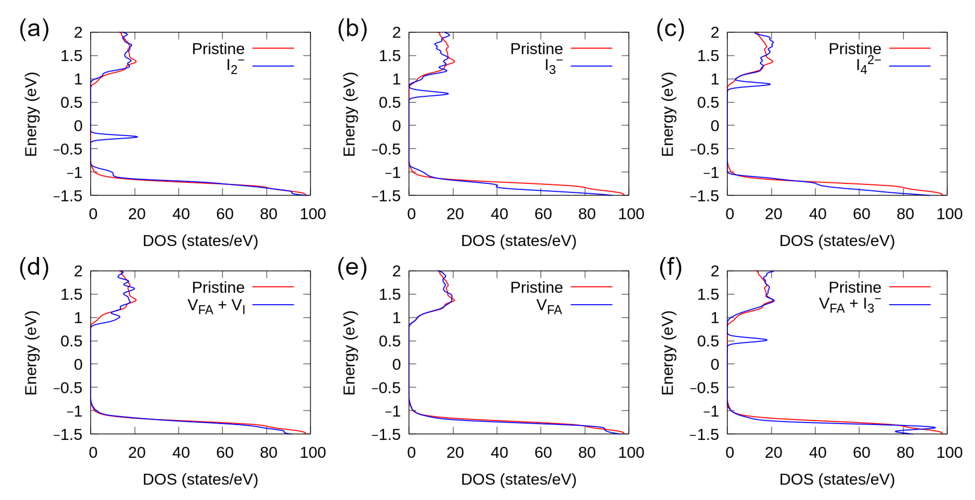
3.5. Density of States

The density of states calculated for each defect structure is presented in Figure 5. Differences between the DOS of the defect-containing and pristine perovskite then represent electronic states that were introduced by defect formation. Excess iodine defects introduce defect states associated with the I to I 0 transition. Iodine dimers, I 2 , are amphoteric with degenerate defect states near the center of the gap [19]. I 2 can adopt the I 2 0 , I 2 , or I 2 2 formal charge depending on whether the Fermi level is below, within, or above the defect states, respectively. On the other hand, the iodine trimer has a nearly-degenerate pair of defect states near the conduction band. Occupation of one defect state changes the charge to I 3 2 , whereas occupation of both states forms I 3 3 . V F A + I 3 exhibits a quite similar, but slightly deeper, pair of degenerate states near the CB. The iodine tetramer similarly shows defect states within the conduction band (CB). V F A + V I + shows a pair of defect states in the CB due to a Pb 2 + to Pb + transition. V F A produces very little change to the density of states, instead behaving as a p-type dopant.

4. Discussion

The reaction enthalpies for Reactions (1)–(7) demonstrate the hierarchy of most-preferential structural motifs for excess iodine introduced into the perovskite. The order of preference is: V F A + I 3 (Reaction (7)), I 4 2 (Reaction (4)), I 3 (Reaction (3)), V F A (Reaction (6)), and I 2 (Reaction (2)). The latter two are energetically unfavorable, but Reaction (6) is nearly isoenergetic. Reaction (7) presupposes the existence of a Schottky defect. The low formation enthalpy of Reaction (7) illustrates how an iodine trimer can partially fill the void created by V F A and support the perovskite lattice. If the material does not have a Schottky defect, then Reactions (4) (I 4 2 ) and (3) (I 3 ) become the most energetically favorable. The formation enthalpy of the trimer and tetramer are within the thermal energy (~25 meV) of one another. However, we expect the iodine tetramer to prevent cation rotation. We have also not observed the expected binding energy signature of the iodine tetramer discussed below. Instead, the iodine trimer stands out as the most likely form. In dye-sensitized solar cells, iodine trimers form a stable component of a redox couple, whereas iodine dimers are metastable [60]. A comparison of Reactions (3) and (5) suggests that iodine trimers form more easily than Schottky defects in pristine perovskite materials.
The most energetically favorable reactions for iodine incorporation result in small changes to the iodine oxidation states. Reaction (7) results in different charges on the two iodine atoms of the I 2 reactant. The first atom retains its I 0 oxidation state as the central atom in an iodine trimer, while the second atom picks up the − 1 2 resonance average, receiving a small charge transfer from the lattice. Reaction (3) produces I 0 and I from the I 2 reactant. Once again, one atom is contributed into the trimer at the same I 0 charge state as molecular iodine. The other atom is reduced to I and binds to the same lead to form a PbI 8 4 polyhedra. We note that both iodine atoms from the original I 2 molecule could become part of the trimer. This would involve less charge transfer from the lattice, but it would require substantial rearrangement. We depict the reaction pathway where the Pb–I bonds of the original corner-sharing motif remain along the path to trimer formation. The trimer defect alters the coordination environment of several adjacent PbI 6 4 octahedra, as well. The octahedra sharing the ends of the trimer are charge excess due to the − 1 2 resonance charge. Similarly, the reduced I from the I 2 reactant leaves an adjacent polyhedra with charge deficiency. No additional chemical environments were observed in DFT calculations containing these altered polyhedra besides the three iodine in the trimer itself. Notably, Reactions (2)–(4) and (7) reduce the number of lattice iodide, I .
While a small number of charged defects can remain in a space charge region, charge-balanced defects can form in larger quantities. Each charged defect increases an energetic penalty for additional defects of the same charge, thereby limiting their concentration. In contrast, the formation energy of dilute charge-balanced defects is essentially concentration-independent. Iodine’s unique position within the lattice allows it to fulfill its octet by ionic or covalent bonding. Defects can be charge-balanced by oxidative or reductive responses within the lattice. Iodide oxidation is observed, whereas we do not see any reduced species in the perovskite lattice. The acid dissociation constant of formamidine (11.5 [61]) indicates a strong base utilized to form the A-site of the perovskite, imbuing thermal and kinetic stability while mitigating the possibility of deprotonation reactions in equilibrium conditions. Moreover, the Bader charge of I found to be −0.72 supports predominant ionic bonding. As additional iodine are introduced to the perovskite lattice and form defects, the tendency towards more covalent bonding character therefore does not strongly redistribute charge on the A-site cation; rather, it redistributes additional electron density among the iodine trimer, for example. Furthermore, the XPS data shows no evidence for the presence of Pb + , Pb 0 , FA 0 , or I + .
Importantly, the reaction enthalpies reveal that certain defects are unstable. For example, the iodine near two A-site vacancies (Figure 1f) is expected to covalently bond to form a Schottky defect ( V F A + V I + , Figure 1e) and an iodine trimer in an A-site vacancy (V F A + I 3 , Figure 1g), the latter of which, V F A , is charge-balanced by the iodine trimer along the edge of the A-site vacancy (cf Reactions (6) and (7)). Similarly, I 3 is more energetically favorable than two I 2 . Thus, it is possible for formamidinium vacancies (V F A ), iodine vacancies (V I ), and iodine trimers (I 3 ) to coexist simultaneously.
Defect levels in the gap often introduce sub-gap absorption features due to the band edge–defect interactions. The simulated defect energy level within the band edge for the Shottky defect is likely to enhance band edge absorption. Our earlier results support that the trimer defect exhibits a high absorption in the blue range from 400 nm to 550 nm in the MHP host material [35]. We note that single particle energy levels were calculated with respect to neutral supercells. The positions of defect states can shift when occupied and generally move away from the center of the gap. Furthermore, whenever defect states are near a band edge, there is potential for coupling between the defect state and the band. In this case, interaction between defect states and bands should be examined with higher-order electronic structure methods to assess whether the state lies within the gap or within the band. Du observed that with hybrid functionals and spin orbit coupling, defect states could move into or out of the gap compared to GGA-PBE even if both methods produce a similar bandgap [62]. Further analysis is needed to evaluate the oscillator strength of the defect-level transitions.
Bader charge analysis reveals drastically different atomic charges between each defect structure, which were used as a basis to differentiate defects through spectroscopic methods. Notably, the iodine trimer, I 3 , contains one atom with the formal charge I 0 (Environment V) and two iodine atoms with a resonance average charge of − 1 2 (Environment IV). The asymmetric ends of the trimer further enrich its spectrum. This gives the trimer a unique signature of three separate atomic charges in a 1:1:1 ratio. If the two ends of the trimer are within the resolution limit of one another, the trimer appears as two different atomic charges in a 2:1 ratio. We observed a ratio of peak 1 to peak 2 of nearly 2:1 for each sample. In comparison, I 2 could produce peak 1 and I 4 2 could produce peaks 0 and 2. However, I 2 is calculated to be unstable compared to I 3 . Moreover, I 4 2 is symmetric and would be expected to produce peak 0 and peak 2 in equal concentrations. Additionally, the Bader charges at the two ends of the tetramer are more similar to one another than the two ends of the trimer. (cf. environments IV and VI). These facts combined support the conclusion that a combination of I 2 and I 4 2 would not produce the observed signal. Instead, the iodine trimer stands out as a reasonable match to the observed data.
Changes to the iodine oxidation state are observable as chemical shifts in the iodine 3d 5 / 2 X-ray photoelectron spectra. Four peaks were observed in the I 3d 5 / 2 spectra when additional iodine was present: the original I peak of pristine perovskite (618.6 eV), peak 0 (618.9 eV), peak 1 (620.06 eV), and peak 2 (620.85 eV). X-ray induced photoelectrons that originate from iodine atoms with a more positive atomic charge are measured at higher BE values. In this regard, peak 1 is assigned to the resonance average charge of − 1 2 coming from environment IV of the iodine trimer. Peak 2 would result from I 0 and environment V of the iodine trimer. The XPS difference spectra of three samples exhibits the trend of atomic charge (binding energy) and relative abundance expected from the I 3 defect by Bader charge analysis.
Identification of chemical species for peak 0 requires additional discussion. The increased signal from I could owe to several distinct sample properties. The first would be the addition of lattice iodine following an increase of I:Pb, assuming I depletion in the reference sample A. The second is possible I 4 2 , as shown in Figure 1d, which is not likely in the measured samples, as discussed in detail above. The third is the reduction of iodine trimers to I 3 2 , which would require a large shift in E F (not observed) to populate enough trimers for observation in XPS. The fourth is the impact of V F A on the I chemical environment would have nearly the right Bader charge prediction. It would be due to weak covalent bonding of iodine surrounding V F A . However, V F A is unlikely to form where excess FA is present. The fifth is the likely presence of non-perovskite organic halide phases due to excess FA cations, which is supported by samples B–D having both increased N:Pb and increased peak 0 areas. Because peak 0 is slightly oxidized relative to the perovskite, it cannot originate from FAI commensurate with the Bader charge analysis. While FAI is unlikely to remain after film formation, and its iodine is reduced relative to the perovskite, substantial FAI excess could in principle-form amorphous FA 2 PbI 4 . This type of second phase inclusion, whether surface-bound or found at grain boundaries is possible, relates to the material crystallinity and cannot be ruled out. Hence, we speculate that peak 0 most likely corresponds to additional lattice iodide filling the small amount of vacancies present in sample A and any surface species, such as second-phase inclusions. This speculation is supported by sample B having both the highest N:Pb and the largest peak 0 area among the samples tested.
There is a clear change in the shape of the I 3d 5 / 2 spectra due to excess iodine that leads to additional photoelectron signal at higher BE. Other examples of shifting I chemical environments have been reported, including dopants that move the I 3d peak positions relative to Pb in XPS [63]. However, this effect is difficult to observe when the Fermi level may also change, and indeed does in the report from [64], where all core levels shift to higher BE values. Analytically, the correction to the Fermi level can be accomplished by shifting the Pb 4f to coincide with a reference spectra, and the spectral changes to the I 3d 5 / 2 become clear and repeatable. Kerner et al. identified similar I 3d features as either I 2 or I 3 during a process designed to generate these species [65]. Mundt et al. fit their mixed-cation perovskite I 3d spectra with one peak for I located at 619.1 eV and one peak for the I 3 at 620.2 eV [66]. The higher binding energy for increasingly covalent iodine atoms occurs owed to the decreased electron density available to the iodine in the defect structure, which lowers the screening effect for the I 3d photoelectrons during the photoemission process. Considering the different fit models and the different perovskite formulations, the similar results are significant and support a broader trend in iodine based perovskites. The further identification of features in I 3d 5 / 2 spectra is especially relevant to the assignment of defects in the samples.

5. Conclusions

Oxidation of iodine from I to I 0 by mixed ionic and covalent bonding is a critical factor allowing for perovskite lattice defects to form in large quantities. Our results show that the I to I 0 transition is responsible for electronically-active defects in MHPs which are observed using chemically sensitive XPS measurements. These results highlight an asymmetry in the types of defects that can form in large quantities. An iodine deficiency must be accompanied by a corresponding A-site deficiency. However, iodine excess can be compensated by iodine oxidation. Conversely, A-site deficiency can be compensated by iodine oxidation, but A-site excess must be compensated by iodine excess. Iodine’s flexibility between the I and I 0 charge states adds degrees of freedom and elasticity to soft perovskite materials. This flexibility stabilizes a range of stoichiometries through the formation of iodine trimers.
Iodine trimers are important to perovskite durability and are observable in XPS measurements. Because these defects are also photoactive [67], need no oxygen or water to react, and their decomposition leads to self-replication, the durability of perovskite with iodine trimers is likely to be low. This was shown in Donakowski et al. under exposure to light in UHV, where the rapid photodecomposition mechanism was elucidated. Regarding expanding the triiodide study to include other halides, our preliminary assessments suggest chloride substitution disfavors trimer formation. We speculate that surface passivation by a higher oxidation potential halide (e.g., Br or Cl) would inhibit I 2 from binding to the perovskite surface. If proven, this could provide a route to mitigating trimer formation and their effects within the perovskite.
Broadly speaking, excess FAI has the potential to improve device performance [68], but also increases the likelihood to form point defects such as I 3 . This combined effect appears to reduce the material durability and poses a significant challenge for technical advancements. The I 3 defect in Cs:FAPI DOS indicates a moderate donor-type property which would shift the Fermi level in the direction of the CB and help to explain how these defects are able to eliminate deep-level electronically active defects [69]. Spectroscopic reference to a particular MHPs formulation or internal standard can be used as a quality control check for perovskite manufacturers, identifying excess halide or other chemical varieties. We anticipate the data treatment process outlined for perovskite spectral analysis to be extendable to other peaks and perovskite systems. The advantages in academic research include deciphering Fermi-level trends in correlation to exact sample growth and processing variables, identification of new spectral signals for particular chemical motifs, and exploring halide charge redistribution for a given metal cation or alloy therof.

Author Contributions

A.R. (Anthony Ruth) and K.X.S. devised the study. E.S. made the samples. A.R. (Anthony Ruth) conducted the simulations. K.X.S. conducted the experiments. A.R. (Anthony Ruth) and K.X.S. drafted the manuscript. All authors analyzed the results, reviewed and commented on the manuscript. All authors refined the analysis and contributed to the final manuscript. All authors have read and agreed to the published version of the manuscript.

Funding

This work is funded by the U.S. Department of Energy Solar Energy Technologies Office, under Award Number DE-EE0008540.

Data Availability Statement

Data available by request.

Conflicts of Interest

Authors Anthony Ruth, Michael Holland, Erin Sanehira, and Michael D. Irwin declare that they are employees at CubicPV which is a commercial entity developing perovskite/silicon tandem modules.

Abbreviations

The following abbreviations are used in this manuscript:
MHPsMetal halide perovskite materials
XPSX-ray photoelectron spectroscopy
BEBinding energy
FWHMFull width half max
VASPVienna Ab Initio Software Package
DFTDensity functional theory
GGA-PBEThe Perdew, Burke, Erzenhof formulation of the generalized gradient approximation
VDWvan der Waals
PAWProjector augmented wave
DOSDensity of states
CBConduction band
VBValence band

References

  1. Zhang, J.; Chen, R.; Wu, Y.; Shang, M.; Zeng, Z.; Zhang, Y.; Zhu, Y.; Han, L. Extrinsic Movable Ions in MAPbI3 Modulate Energy Band Alignment in Perovskite Solar Cells. Adv. Energy Mater. 2018, 8, 1701981. [Google Scholar] [CrossRef]
  2. Liu, N.; Yam, C. First-principles study of intrinsic defects in formamidinium lead triiodide perovskite solar cell absorbers. Phys. Chem. Chem. Phys. 2018, 20, 6800–6804. [Google Scholar] [CrossRef]
  3. Miller, D.W.; Eperon, G.E.; Roe, E.T.; Warren, C.W.; Snaith, H.J.; Lonergan, M.C. Defect states in perovskite solar cells associated with hysteresis and performance. Appl. Phys. Lett. 2016, 109, 153902. [Google Scholar] [CrossRef]
  4. Kim, H.S.; Jang, I.H.; Ahn, N.; Choi, M.; Guerrero, A.; Bisquert, J.; Park, N.G. Control of IV Hysteresis CH3NH3PbI3 Perovskite Solar Cell. J. Phys. Chem. Lett. 2015, 6, 4633–4639. [Google Scholar] [CrossRef]
  5. Calado, P.; Telford, A.M.; Bryant, D.; Li, X.; Nelson, J.; O’Regan, B.C.; Barnes, P.R.F. Evidence for ion migration in hybrid perovskite solar cells with minimal hysteresis. Nat. Commun. 2016, 7, 13831. [Google Scholar] [CrossRef]
  6. Zarazua, I.; Bisquert, J.; Garcia-Belmonte, G. Light-Induced Space-Charge Accumulation Zone as Photovoltaic Mechanism in Perovskite Solar Cells. J. Phys. Chem. Lett. 2016, 7, 525–528. [Google Scholar] [CrossRef] [Green Version]
  7. Moia, D.; Gelmetti, I.; Calado, P.; Fisher, W.; Stringer, M.; Game, O.; Hu, Y.; Docampo, P.; Lidzey, D.; Palomares, E.; et al. Ionic-to-electronic current amplification in hybrid perovskite solar cells: Ionically gated transistor-interface circuit model explains hysteresis and impedance of mixed conducting devices. Energy Environ. Sci. 2019, 12, 1296–1308. [Google Scholar] [CrossRef]
  8. Watts, C.L.; Aspitarte, L.; Lin, Y.H.; Li, W.; Elzein, R.; Addou, R.; Hong, M.J.; Herman, G.S.; Snaith, H.J.; Labram, J.G. Light soaking in metal halide perovskites studied via steady-state microwave conductivity. Commun. Phys. 2020, 3, 73. [Google Scholar] [CrossRef]
  9. Mosconi, E.; Meggiolaro, D.; Snaith, H.J.; Stranks, S.D.; De Angelis, F. Light-induced annihilation of Frenkel defects in organo-lead halide perovskites. Energy Environ. Sci. 2016, 9, 3180–3187. [Google Scholar] [CrossRef]
  10. Knight, A.J.; Wright, A.D.; Patel, J.B.; McMeekin, D.P.; Snaith, H.J.; Johnston, M.B.; Herz, L.M. Electronic Traps and Phase Segregation in Lead Mixed-Halide Perovskite. ACS Energy Lett. 2019, 4, 75–84. [Google Scholar] [CrossRef]
  11. Brennan, M.C.; Ruth, A.; Kamat, P.V.; Kuno, M. Photoinduced anion segregation in mixed Halide perovskites. Trends Chem. 2020, 2, 282–301. [Google Scholar] [CrossRef] [Green Version]
  12. Hoke, E.T.; Slotcavage, D.J.; Dohner, E.R.; Bowring, A.R.; Karunadasa, H.I.; McGehee, M.D. Reversible photo-induced trap formation in mixed-halide hybrid perovskites for photovoltaics. Chem. Sci. 2015, 6, 613–617. [Google Scholar] [CrossRef] [PubMed] [Green Version]
  13. Kerner, R.A.; Rand, B.P. Ionic–Electronic Ambipolar Transport in Metal Halide Perovskites: Can Electronic Conductivity Limit Ionic Diffusion? J. Phys. Chem. Lett. 2018, 9, 132–137. [Google Scholar] [CrossRef] [PubMed]
  14. Chen, Y.; Zhou, H. Defects chemistry in high-efficiency and stable perovskite solar cells. J. Appl. Phys. 2020, 128, 060903. [Google Scholar] [CrossRef]
  15. Yang, J.H.; Yin, W.J.; Park, J.S.; Wei, S.H. Fast self-diffusion of ions in CH3NH3PbI3: The interstiticaly mechanism versus vacancy-assisted mechanism. J. Mater. Chem. A 2016, 4, 13105–13112. [Google Scholar] [CrossRef]
  16. Eames, C.; Frost, J.M.; Barnes, P.R.F.; O’Regan, B.C.; Walsh, A.; Islam, M.S. Ionic transport in hybrid lead iodide perovskite solar cells. Nat. Commun. 2015, 6, 7497. [Google Scholar] [CrossRef] [Green Version]
  17. Ruth, A.; Brennan, M.C.; Draguta, S.; Morozov, Y.V.; Zhukovskyi, M.; Janko, B.; Zapol, P.; Kuno, M. Vacancy-Mediated Anion Photosegregation Kinetics in Mixed Halide Hybrid Perovskites: Coupled Kinetic Monte Carlo and Optical Measurements. ACS Energy Lett. 2018, 3, 2321–2328. [Google Scholar] [CrossRef]
  18. Rothmann, M.U.; Kim, J.S.; Borchert, J.; Lohmann, K.B.; O’Leary, C.M.; Sheader, A.A.; Clark, L.; Snaith, H.J.; Johnston, M.B.; Nellist, P.D.; et al. Atomic-scale microstructure of metal halide perovskite. Science 2020, 370, eabb5940. [Google Scholar] [CrossRef] [PubMed]
  19. Meggiolaro, D.; Mosconi, E.; De Angelis, F. Modeling the Interaction of Molecular Iodine with MAPbI3: A Probe of Lead-Halide Perovskites Defect Chemistry. ACS Energy Lett. 2018, 3, 447–451. [Google Scholar] [CrossRef]
  20. Walsh, A.; Scanlon, D.O.; Chen, S.; Gong, X.G.; Wei, S. Self-Regulation Mechanism for Charged Point Defects in Hybrid Halide Perovskites. Angew. Chem. Int. Ed. 2015, 54, 1791–1794. [Google Scholar] [CrossRef] [PubMed] [Green Version]
  21. Evarestov, R.A.; Senocrate, A.; Kotomin, E.A.; Maier, J. First-principles calculations of iodine-related point defects in CsPbI 3. Phys. Chem. Chem. Phys. 2019, 21, 7841–7846. [Google Scholar] [CrossRef]
  22. Meggiolaro, D.; Mosconi, E.; De Angelis, F. Formation of Surface Defects Dominates Ion Migration in Lead-Halide Perovskites. ACS Energy Lett. 2019, 4, 779–785. [Google Scholar] [CrossRef] [Green Version]
  23. Wang, F.; Bai, S.; Tress, W.; Hagfeldt, A.; Gao, F. Defects engineering for high-performance perovskite solar cells. NPJ Flex. Electron. 2018, 2, 22. [Google Scholar] [CrossRef] [Green Version]
  24. Samu, G.F.; Balog, A.; De Angelis, F.; Meggiolaro, D.; Kamat, P.V.; Janáky, C. Electrochemical Hole Injection Selectively Expels Iodide from Mixed Halide Perovskite Films. J. Am. Chem. Soc. 2019, 141, 10812–10820. [Google Scholar] [CrossRef] [PubMed] [Green Version]
  25. Park, J.S.; Calbo, J.; Jung, Y.K.; Whalley, L.D.; Walsh, A. Accumulation of Deep Traps at Grain Boundaries in Halide Perovskites. ACS Energy Lett. 2019, 4, 1321–1327. [Google Scholar] [CrossRef]
  26. Naskar, A.; Khanal, R.; Choudhury, S. Role of Chemistry and Crystal Structure on the Electronic Defect States in Cs-Based Halide Perovskites. Materials 2021, 14, 1032. [Google Scholar] [CrossRef] [PubMed]
  27. Das, C.; Wussler, M.; Hellmann, T.; Mayer, T.; Jaegermann, W. In situ XPS study of the surface chemistry of MAPI solar cells under operating conditions in vacuum. Phys. Chem. Chem. Phys. 2018, 20, 17180–17187. [Google Scholar] [CrossRef] [PubMed]
  28. Doherty, T.A.S.; Winchester, A.J.; Macpherson, S.; Johnstone, D.N.; Pareek, V.; Tennyson, E.M.; Kosar, S.; Kosasih, F.U.; Anaya, M.; Abdi-Jalebi, M.; et al. Performance-limiting nanoscale trap clusters at grain junctions in halide perovskites. Nature 2020, 580, 360–366. [Google Scholar] [CrossRef] [PubMed]
  29. Reichert, S.; An, Q.; Woo, Y.W.; Walsh, A.; Vaynzof, Y.; Deibel, C. Probing the ionic defect landscape in halide perovskite solar cells. Nat. Commun. 2020, 11, 6098. [Google Scholar] [CrossRef]
  30. Steirer, K.X.; Schulz, P.; Teeter, G.; Stevanovic, V.; Yang, M.; Zhu, K.; Berry, J.J. Defect Tolerance in Methylammonium Lead Triiodide Perovskite. ACS Energy Lett. 2016, 1, 360–366. [Google Scholar] [CrossRef]
  31. Park, B.w.; Kwon, H.W.; Lee, Y.; Lee, D.Y.; Kim, M.G.; Kim, G.; Kim, K.j.; Kim, Y.K.; Im, J.; Shin, T.J.; et al. Stabilization of formamidinium lead triiodide α-phase with isopropylammonium chloride for perovskite solar cells. Nat. Energy 2021, 6, 419–428. [Google Scholar] [CrossRef]
  32. Cacovich, S.; Messou, D.; Bercegol, A.; Béchu, S.; Yaiche, A.; Shafique, H.; Rousset, J.; Schulz, P.; Bouttemy, M.; Lombez, L. Light-Induced Passivation in Triple Cation Mixed Halide Perovskites: Interplay between Transport Properties and Surface Chemistry. ACS Appl. Mater. Interfaces 2020, 12, 34784–34794. [Google Scholar] [CrossRef]
  33. Boyd, C.C.; Shallcross, R.C.; Moot, T.; Kerner, R.; Bertoluzzi, L.; Onno, A.; Kavadiya, S.; Chosy, C.; Wolf, E.J.; Werner, J.; et al. Overcoming Redox Reactions at Perovskite-Nickel Oxide Interfaces to Boost Voltages in Perovskite Solar Cells. Joule 2020, 4, 1759–1775. [Google Scholar] [CrossRef]
  34. Kot, M.; Kegelmann, L.; Köbler, H.; Vorokhta, M.; Escudero, C.; Kúš, P.; Šmíd, B.; Tallarida, M.; Albrecht, S.; Abate, A.; et al. In situ Near-Ambient Pressure X-ray Photoelectron Spectroscopy Reveals the Influence of Photon Flux and Water on the Stability of Halide Perovskite. ChemSusChem 2020, 13, 5722–5730. [Google Scholar] [CrossRef]
  35. Donakowski, A.; Miller, D.W.; Anderson, N.C.; Ruth, A.; Sanehira, E.M.; Berry, J.J.; Irwin, M.D.; Rockett, A.; Steirer, K.X. Improving Photostability of Cesium-Doped Formamidinium Lead Triiodide Perovskite. ACS Energy Lett. 2021, 6, 574–580. [Google Scholar] [CrossRef]
  36. Haruyama, J.; Sodeyama, K.; Han, L.; Tateyama, Y. Surface Properties of CH3NH3PbI3 for Perovskite Solar Cells. Acc. Chem. Res. 2016, 49, 554–561. [Google Scholar] [CrossRef] [PubMed]
  37. Weller, M.T.; Weber, O.J.; Frost, J.M.; Walsh, A. Cubic Perovskite Structure of Black Formamidinium Lead Iodide, α-[HC(NH2)2]PbI3, at 298 K. J. Phys. Chem. Lett. 2015, 6, 3209–3212. [Google Scholar] [CrossRef]
  38. Dalpian, G.M.; Zhao, X.G.; Kazmerski, L.; Zunger, A. Formation and Composition-Dependent Properties of Alloys of Cubic Halide Perovskites. Chem. Mater. 2019, 31, 2497–2506. [Google Scholar] [CrossRef] [Green Version]
  39. Kim, J.; Lee, S.H.; Lee, J.H.; Hong, K.H. The Role of Intrinsic Defects in Methylammonium Lead Iodide Perovskite. J. Phys. Chem. Lett. 2014, 5, 1312–1317. [Google Scholar] [CrossRef] [PubMed]
  40. Bader, R.F. Atoms in Molecules: A Quantum Theory; Clarendon Pr Oxford: Cary, NC, USA, 1990. [Google Scholar]
  41. Code: Bader Charge Analysis. Available online: http://theory.cm.utexas.edu/henkelman/code/bader/ (accessed on 19 December 2021).
  42. Kerner, R.A.; Xu, Z.; Larson, B.W.; Rand, B.P. The role of halide oxidation in perovskite halide phase separation. Joule 2021, 5, 2273–2295. [Google Scholar] [CrossRef]
  43. Irwin, M.D.; Dhas, V.V.; Mielczarek, K. Doped Nickel Oxide Interfacial Layer. U.S. Patent 10189998B2, 29 January 2019. [Google Scholar]
  44. Irwin, M.D.; Chute, J.A.; Dhas, V.V. Method of Formulating Perovskite Solar Cell Materials. U.S. Patent 9305715B2, 5 April 2016. [Google Scholar]
  45. Irwin, M.D.; Chute, J.A.; Dhas, V.V. Perovskite Material Layer Processing. U.S. Patent 9425396B2, 23 August 2016. [Google Scholar]
  46. Irwin, M.D.; Chute, J.A.; Dhas, V.V.; Mielczarek, K. Mixed Cation Perovskite Material Devices. U.S. Patent 10316196B2, 11 June 2019. [Google Scholar]
  47. Blöchl, P.E. Projector augmented-wave method. Phys. Rev. B 1994, 50, 17953–17979. [Google Scholar] [CrossRef] [PubMed] [Green Version]
  48. Kresse, G.; Joubert, D. From ultrasoft pseudopotentials to the projector augmented-wave method. Phys. Rev. B 1999, 59, 1758–1775. [Google Scholar] [CrossRef]
  49. Perdew, J.P.; Burke, K.; Ernzerhof, M. Generalized Gradient Approximation Made Simple. Phys. Rev. Lett. 1996, 77, 3865–3868. [Google Scholar] [CrossRef] [PubMed] [Green Version]
  50. Pack, J.D.; Monkhorst, H.J. “Special points for Brillouin-zone integrations”—A reply. Phys. Rev. B 1977, 16, 1748–1749. [Google Scholar] [CrossRef]
  51. Pavlovetc, I.M.; Brennan, M.C.; Draguta, S.; Ruth, A.; Moot, T.; Christians, J.A.; Aleshire, K.; Harvey, S.P.; Toso, S.; Nanayakkara, S.U.; et al. Suppressing Cation Migration in Triple-Cation Lead Halide Perovskites. ACS Energy Lett. 2020, 5, 2802–2810. [Google Scholar] [CrossRef]
  52. Li, Z.; Yang, M.; Park, J.S.; Wei, S.H.; Berry, J.J.; Zhu, K. Stabilizing Perovskite Structures by Tuning Tolerance Factor: Formation of Formamidinium and Cesium Lead Iodide Solid-State Alloys. Chem. Mater. 2016, 28, 284–292. [Google Scholar] [CrossRef]
  53. Zhao, X.G.; Dalpian, G.M.; Wang, Z.; Zunger, A. Polymorphous nature of cubic halide perovskites. Phys. Rev. B 2020, 101, 155137. [Google Scholar] [CrossRef]
  54. MedeA. Available online: https://www.materialsdesign.com/ (accessed on 19 December 2021).
  55. Lide, D.R. Handbook of Chemistry and Physics: CRC Handbook; CRC Press: Boca Raton, FL, USA, 1993. [Google Scholar]
  56. Csm-Xps. minespex. Available online: https://github.com/csm-xps/minespex (accessed on 19 December 2021).
  57. Schulz, P.; Whittaker-Brooks, L.L.; MacLeod, B.A.; Olson, D.C.; Loo, Y.L.; Kahn, A. Electronic Level Alignment in Inverted Organometal Perovskite Solar Cells. Adv. Mater. Interfaces 2015, 2, 1400532. [Google Scholar] [CrossRef]
  58. Heo, S.; Seo, G.; Lee, Y.; Lee, D.; Seol, M.; Lee, J.; Park, J.B.; Kim, K.; Yun, D.J.; Kim, Y.S.; et al. Deep level trapped defect analysis in CH3NH3PbI3 perovskite solar cells by deep level transient spectroscopy. Energy Environ. Sci. 2017, 10, 1128–1133. [Google Scholar] [CrossRef]
  59. Kearney, K.; Seo, G.; Matsushima, T.; Adachi, C.; Ertekin, E.; Rockett, A. Computational Analysis of the Interplay between Deep Level Traps and Perovskite Solar Cell Efficiency. J. Am. Chem. Soc. 2018, 140, 15655–15660. [Google Scholar] [CrossRef]
  60. Sharma, K.; Sharma, V.; Sharma, S.S. Dye-Sensitized Solar Cells: Fundamentals and Current Status. Nanoscale Res. Lett. 2018, 13, 381. [Google Scholar] [CrossRef]
  61. Luongo, A.; Brunetti, B.; Vecchio Ciprioti, S.; Ciccioli, A.; Latini, A. Thermodynamic and Kinetic Aspects of Formamidinium Lead Iodide Thermal Decomposition. J. Phys. Chem. C 2021, 125, 21851–21861. [Google Scholar] [CrossRef] [PubMed]
  62. Du, M.H. Density Functional Calculations of Native Defects in CH3NH3PbI3: Effects of Spin–Orbit Coupling and Self-Interaction Error. J. Phys. Chem. Lett. 2015, 6, 1461–1466. [Google Scholar] [CrossRef] [PubMed]
  63. Wang, L.; Zhou, H.; Hu, J.; Huang, B.; Sun, M.; Dong, B.; Zheng, G.; Huang, Y.; Chen, Y.; Li, L.; et al. A Eu3+-Eu2+ ion redox shuttle imparts operational durability to Pb-I perovskite solar cells. Science 2019, 363, 265–270. [Google Scholar] [CrossRef] [PubMed]
  64. Zhidkov, I.S.; Boukhvalov, D.W.; Akbulatov, A.F.; Frolova, L.A.; Finkelstein, L.D.; Kukharenko, A.I.; Cholakh, S.O.; Chueh, C.C.; Troshin, P.A.; Kurmaev, E.Z. XPS spectra as a tool for studying photochemical and thermal degradation in APbX3 hybrid halide perovskites. Nano Energy 2021, 79, 105421. [Google Scholar] [CrossRef]
  65. Kerner, R.A.; Schulz, P.; Christians, J.A.; Dunfield, S.P.; Dou, B.; Zhao, L.; Teeter, G.; Berry, J.J.; Rand, B.P. Reactions at noble metal contacts with methylammonium lead triiodide perovskites: Role of underpotential deposition and electrochemistry. APL Mater. 2019, 7, 041103. [Google Scholar] [CrossRef]
  66. Mundt, L.E.; Tong, J.; Palmstrom, A.F.; Dunfield, S.P.; Zhu, K.; Berry, J.J.; Schelhas, L.T.; Ratcliff, E.L. Surface-Activated Corrosion in Tin–Lead Halide Perovskite Solar Cells. ACS Energy Lett. 2020, 5, 3344–3351. [Google Scholar] [CrossRef]
  67. Boschloo, G.; Hagfeldt, A. Characteristics of the Iodide/Triiodide Redox Mediator in Dye-Sensitized Solar Cells. Acc. Chem. Res. 2009, 42, 1819–1826. [Google Scholar] [CrossRef]
  68. Jia, Y.H.; Neutzner, S.; Zhou, Y.; Yang, M.; Tapia, J.M.F.; Li, N.; Yu, H.; Cao, J.; Wang, J.P.; Petrozza, A.; et al. Role of Excess FAI in Formation of High-Efficiency FAPbI3-Based Light-Emitting Diodes. Adv. Funct. Mater. 2020, 30, 1906875. [Google Scholar] [CrossRef]
  69. Yang, W.S.; Park, B.W.; Jung, E.H.; Jeon, N.J.; Kim, Y.C.; Lee, D.U.; Shin, S.S.; Seo, J.; Kim, E.K.; Noh, J.H.; et al. Iodide management in formamidinium-lead-halide–based perovskite layers for efficient solar cells. Science 2017, 356, 1376–1379. [Google Scholar] [CrossRef] [Green Version]
Figure 1. Polymorphic defect structures of FAPbI 3 . A black box in panel (a) illustrates the 2 × 2 × 2 supercell used in all calculations. In each case, a 4 × 4 grid of FA molecules and 3 × 3 grid of polyhedra is shown. (a) Pristine FAPbI 3 , (b) iodine dimer (I 2 ), (c) iodine trimer (I 3 ), (d) iodine tetramer (I 4 2 ), (e) Schottky defect (V F A + V I + ), (f) formamidinium vacancy (V F A ), (g) iodine trimer in formamidinium vacancy (V F A + I 3 ). Polyhedra indicate the lead iodide lattice. Red atoms illustrate the location of FA or I prior to removal in order to form vacancies. Green atoms were added to form defects. Iodine–iodine covalent bonds are shown as green bars. Depth cueing indicates the foreground and background atoms.
Crystals 12 00088 g001
Figure 2. Chemical environments of iodine in defect structures. (I) Iodine branching two corner-sharing octahedra as in pristine perovskite, (II) iodine surrounding V F A , (III) iodine dimer, (IV) end of iodine trimer, (V) middle of iodine trimer, (VI) end of iodine tetramer, (VII) middle of iodine tetramer. Depth cueing indicates the foreground and background atoms.
Crystals 12 00088 g002
Figure 3. Characteristic measured and processed spectra for Pb 4f and I 3d 5 / 2 difference spectra treated as described in the Methods section. Process routine is illustrated. (a) As-measured Pb 4f core level XPS spectra for samples A and B. (b) Pb 4f spectra divided by total area for each curve. BE is shifted for sample B to align main peak. Difference spectra shown for sample B minus sample A. (c) As-measured I 3d 5 / 2 core level XPS spectra for samples A and B. (d) I 3d 5 / 2 spectra divided by total Pb 4f area. BE is shifted for sample B by same amount as in panel (b). Difference spectra shown for sample B minus sample A. Data shown is reprinted (adapted) from supporting information Figure S4 with permission from [35] Copyright 2021 American Chemical Society.
Crystals 12 00088 g003
Figure 4. Fitted I 3d 5 / 2 difference spectra treated as described in the Methods section. Residuals and individual peak models are shown. (a) Average spectra calculated from samples B, C, and D. (bd) Difference spectra for each sample B–D, respectively.
Crystals 12 00088 g004
Figure 5. Density of states of each defect structure compared to the pristine perovskite. (a) iodine dimer (I 2 ), (b) iodine trimer (I 3 ), (c) iodine tetramer (I 4 2 ), (d) Schottky defect (V F A + V I + ), (e) formamidinium vacancy (V F A ), (f) iodine trimer in formamidinium vacancy (V F A + I 3 ). Features present in the DOS of defect structures but not in the pristine perovskite represent defect states introduced by defect formation.
Crystals 12 00088 g005
Table 1. Bader charge for each iodine chemical environment in associated defect structures.
Iodine EnvironmentDefectDFT StructureBader Charge
IPristinea–g−0.57
IIV F A f−0.50
IIII i b−0.34, −0.31
IVI 3 c−0.36, −0.26
V F A + I 3 g−0.34, −0.23
VI 3 c−0.04
V F A + I 3 g0.00
VII 4 2 d−0.47, −0.45
VIII 4 2 d−0.12, −0.11
Table 2. Lead-based atomic ratios for iodine and nitrogen in perovskite films considered in spectral analyses.
SampleI:PbN:Pb
A2.92.0
B3.52.9
C3.62.5
D3.62.6
Table 3. Three-peak model of I 3d 5 / 2 difference spectra for high iodine samples. The position of peak 1 was fixed to 620.06 eV. The FWHM of each peak was fixed to 1.0 eV. The peaks are assigned to iodine chemical environments, and associated Bader charges of DFT structures are included for reference. Reported error values are correlative error from fits.
PeakBEAssignmentBader (q) δ from Pb 4f 7 / 2 137.75 eVArea
Peak 0618.90 ± 0.03I −0.57481.140.040 ± 0.010
Peak 1620.06I 3 (IV)−0.26, −0.36482.310.0165 ± 0.0028
Peak 2620.85 ± 0.05I 3 (V)−0.04483.110.0082 ± 0.0022
Publisher’s Note: MDPI stays neutral with regard to jurisdictional claims in published maps and institutional affiliations.

