Article

Growth and Characterisation of Layered (BA)2CsAgBiBr7 Double Perovskite Single Crystals for Application in Radiation Sensing

1
Freiburg Materials Research Center, Albert-Ludwigs-Universität Freiburg, Stefan-Meier-Str. 21, 79104 Freiburg im Breisgau, Germany
2
Institute of Inorganic and Analytical Chemistry, Faculty of Chemistry and Pharmacy, Albert-Ludwigs-Universität Freiburg, Albert Str. 21, 79104 Freiburg im Breisgau, Germany
3
Institute of Physics, Faculty of Mathematics and Physics, Charles University, Ke Karlovu 5, CZ-121 16 Prague, Czech Republic
*
Author to whom correspondence should be addressed.
Crystals 2021, 11(10), 1208; https://doi.org/10.3390/cryst11101208
Submission received: 6 September 2021 / Revised: 28 September 2021 / Accepted: 4 October 2021 / Published: 7 October 2021
(This article belongs to the Special Issue Advances in Halide Perovskite Materials)

Abstract

:
A recent publication on single crystals of two-dimensional, layered organic–inorganic (BA)2CsAgBiBr7 double perovskite (BA+ = C H 3 C H 2 3 N H 3 + ) suggested the great potential of this semiconductor material in the detection of X-ray radiation. Our powder XRD measurement confirms the crystallinity and purity of all samples that crystallise in the monoclinic space group P 2 1 / m , while the single crystal XRD measurements reveal the dominant {001} lattice planes. The structure–property relationship is reflected in the lower resistivity values determined from the van der Pauw measurements (1.65–9.16 × 10¹⁰ Ωcm) compared to those determined from the IV measurements (4.19 × 10¹¹–2.67 × 10¹² Ωcm). The density of trap states and charge-carrier mobilities, which are determined from the IV measurements, are 1.12–1.76 × 1011 cm–3 and 10−5–10−4 cm2V–1s–1, respectively. The X-ray photoresponse measurements indicate that the (BA)2CsAgBiBr7 samples synthesised in this study satisfy the requirements for radiation sensors. Further advances in crystal growth are required to reduce the density of defects and improve the performance of single crystals.

Graphical Abstract

1. Introduction

X-ray security screening and medical diagnostic devices require radiation sensors with high resistivity ρ, enhanced charge-carrier mobility μ and collection efficiency to achieve higher sensitivity and lower detection limits. The inorganic, three-dimensional (3D) double perovskite Cs2AgBiBr6 radiation sensor is a stable substitute for the organic–inorganic lead-bearing perovskite MAPbBr3 [1,2,3,4,5,6] due to its higher moisture resistance, suppressed ion migration, absence of toxic lead, presence of heavier constituent elements and consequently higher stopping power [7,8,9,10,11,12]. Indeed, single crystals of Cs2AgBiBr6 with an indirect band gap E G of ca. 2.1 eV demonstrate higher ρ (109–1011 Ωcm), similar density of trap states ntrap (109–1010 cm–3), modest µ (0.5–12 cm2V–1s–1) and a lower mobility-lifetime product μτ (2.48–5.95 × 10⁻³ cm2V−1) but comparable sensitivity and detection limits of 105–1974 μCGyair−1 cm–2 and 45.7–59.7 nGyairs−1, respectively [7,8,9,10,11,12]. This impressive performance stems from its chemical composition and cubic crystal structure (space group Fm 3 ¯ m).
To further suppress ion migration in single crystals of Cs2AgBiBr6 and in turn increase ρ, their 3D structural dimensionality can be lowered to 2D dimensionality by incorporating n-butylammonium cations (n-butylammonium BA+ = C H 3 C H 2 3 N H 3 + ) to produce layered organic–inorganic (BA)2CsAgBiBr7 double perovskite single crystals with monoclinic symmetry, space group P 2 1 / m and an indirect E G of 2.08–2.38 eV [13,14]. The BA+ cations are bound to the [ AgBr 6 ] 5   and [ BiBr 6 ] 3 octahedra and form a barrier layer between the adjacent bilayers of perovskite network with the Cs+ cations in the A-crystallographic site (Figure 1). However, significant distortion—especially of the Ag octahedra—characterises this compound.
Recently synthesised single crystals of the BA 2 CsAgBiBr 7 have ρ of ca. 1.5 × 10¹¹ Ωcm and ntrap of 4.2 × 1010 cm−3, and they exhibit a µτ of 1.21 × 10⁻³ cm2V−1 [14]. The optimised Au/2 mm thick (BA)2CsAgBiBr7/Au detector with the (001) crystal plane parallel to the sample surface has yielded sensitivity of 4.2 μCGyair −1 cm–2. Although the (BA)2CsAgBiBr7 single crystal has demonstrated an encouraging performance, this record is still incomplete, necessitating further studies on the microstructures and structure–property relationships, including an assessment of its suitability as a radiation sensor. Here, we report crystal growth that yielded citron-yellow coloured ca. 3 × 4 × 0.75 mm3 single crystals of (BA)2CsAgBiBr7 with pinacoid form and pseudo-rectangular crystal surfaces with (001) lattice places reflecting two-fold symmetry. We discuss the key electrical performance parameters obtained from the current–voltage (IV) measurements, the space charge limit current (SCLC) and the van der Pauw methods. Specifically, for the four samples, the ρ values that were determined from the IV measurements along the <001> direction (4.19 × 10¹¹–2.67 × 10¹² Ωcm) are one order of magnitude higher than those from the van der Pauw measurements performed along the edges of the pseudo-rectangular crystal faces (1.65–9.16 × 10¹⁰ Ωcm); this difference reflects the structure–property relationship of this semiconductor material. The ntrap and μ, which were calculated from the IV characteristic curve measurements, are 1.12–1.76 × 1011 cm–3 and 10−5–10−4 cm2V–1s–1, respectively. The ρ values along the <001> direction, including the ntrap values, are slightly higher than the published values [14]. The X-ray photoresponse measurements indicate that the (BA)2CsAgBiBr7 samples synthesised in this research study satisfy the requirements for radiation sensors.

2. Materials and Methods

Initial synthesis of the BA 2 CsAgBiBr 7 single crystals closely followed the method described by Xu et al. [14]. However, it yielded ingrown crystal platelets, and the growth procedure was accordingly modified. Seed crystals were prepared from a 66 mM solution that was cooled down to 33 °C at 0.6 °C/h, because needles of an unknown compound formed at temperatures T below 30 °C. Large crystals were grown from a 66 mM solution prepared by dissolving CsBr (0.94 g, Aldrich Chemical, WI, USA), AgBr (0.864 g, AlfaAesar, MA, USA) and Bi2O3 (1.040 g, ChemPur, Karlsruhe, Germany) in boiling HBr (29 ml 48 w%, Acros Chemicals, Geel, Belgium) with n-butylamine C4H11N (14.5 ml, 10.7 g). A small excess of the precursor AgBr was added to supress formation of the by-product phase Cs3Bi2Br9. To dissolve and therefore smoothen the surfaces of an added seed crystal, the solution was heated at 90 °C for 30 min. Successful growth of even larger crystals was achieved by adding sodium acetate NaOAc (1 equivalent, C2H3NaO2) as an additive [15]. The solution was cooled down from 80 °C to 60 °C at a constant rate of 0.24°C/h, then heated isothermally at 60°C for 3 days, and finally cooled down to 33 °C at 0.6 °C/h in a closed oven. This growth method yielded higher quality citron-yellow coloured, semitransparent (BA)2CsAgBiBr7 single crystals ca. 3 × 4 × 0.75 mm3 with flat, pseudo-rectangular surfaces but with a tendency to break and crumble along the edges.
A digital reflected-light microscope Keyence VHX-5000 and a differential interference-contrast microscope Zeiss Axio Imager (NY, USA), which was adjusted to transmitted light, were used to examine microstructural features in the crystals.
The STOE STADI P transmission diffractometer (Darmstadt, Germany) was used to acquire powder X-ray diffraction (PXRD) patterns of samples. This diffractometer was equipped with a filtered Mo-Kα1 radiation (λ of 0.7093 Å), curved Ge (111) monochromators and a MYTHEN 1K silicon microstrip detector (Baden, Switzerland). The setup included the Debye–Scherrer scan mode, a fixed sample and the detector. The STOE WinXPOW software program was used to process data.
Single crystal XRD measurements were performed using the Bruker D8 Discover diffractometer (MA, USA). This device features a high-resolution Cu- radiation source (λ of 1.54060 Å Kα1 and λ of 1.54439 Å 2); a focusing Goebel mirror as the primary monochromator, including an 18 mm antiscatter slit and a 0.5 mm divergence slit in a fixed mode; and a line focus silicon-strip detector (LynxEye Xe). The generator was set to 40 mA and 40 kV. The XRD data acquisition and processing were performed using Bruker Diffrac.EVA software® and Crystal Impact Match! software.
Electrical characterisation measurements were carried out using the Keithley source meter unit SMU 2450 and an electrometer model 6517B, including a shielded test fixture model 8101-4TRX to minimise electrostatic interferences by shielding and to control the leakage current in the cables and connectors by guarding. The evaluation of the ohmic behaviour of the Ag glue-(BA)2CsAgBiBr contacts (Figure S1a) from the IV characteristic curves, including the estimation of ρ, trap-filled limit voltage VTFL and hence μ and ntrap, was performed by applying the space charge limited current (SCLM) method [16,17,18,19,20,21,22,23]. The specific ρ values along the edges of a crystal face were determined from the van der Pauw method (Figure S1b). The area of Ag glue electrodes deposited on a crystal surface was estimated to be 0.0227 cm2. It was assumed that the contacts do not inject charge carriers at applied biases. Measurements were carried out using the Keithley model 6517B electrometer and the SMU 2450 in different configurations (a voltmeter, an ammeter and a voltage/current source). All measurements were repeated at least twice to ensure stability of the Keithley devices and, in turn, the reproducibility of recorded values.
The IV curves were measured in an applied bias range from 0 V to ± 100 V for a forward scan (the top crystal face T (+) bottom crystals face B (−) configuration) and for a reverse scan (the T (−) B (+) configuration), with 0 s, 5 s, 10 s, 15 s, 20 s and 25 s source delay times between voltage steps of 1 V and 3 min between the change of an applied bias direction. In the low-voltage range, IV curves follow Ohm’s law (a linear dependence of I on V), whereas in the mid-voltage range, a trap-filled (TFL) regime develops due to the presence of electronic trap states. Consequently, in a log–log plot IV curves have a slope of more than 2 [20]. The n t r a p are calculated from the relationship:
V T F L = q   n t r a p L 2 / ε o ε r
where L is the sample thickness, while ε o   and   ε r are the vacuum and relative dielectric constants, respectively [21]. In a high-voltage range, the injected free carriers fill up all the traps. Hence, a trap-free regime develops, and the current is limited by the build-up of space charge. The IV curves in a log–log plot the have a slope of 2 [17] and the current density follows the Mott–Gurney law:
J = ( 9 / 8 )   μ ε o ε r ( V ) 2 / L 3 )
where J is the current density and V = V T F L [18,22]. Hence,
μ = ( 8 / 9 ) J   L 3 / V T F L 2 ε o ε r
Most publications report the value of n t r a p calculated using the V T F L derived from the crossing point between the tangent of the ohmic IV regime and the TFL IV regime. A more accurate value can be obtained from the V T F L derived from the intersection between the SCLC IV regime and the TFL IV regime [23]. From the IV measurements conducted at different source delay times, it is inferred that the IV curves measured at a 20 s delay time reveal the three regimes required to estimate reliable ρ , V T F L , μ and n t r a p values.
The X-ray photoresponse measurements were carried out on the sample Exp4 using the X-ray tube with a beam source of the RQR6 quality (tungsten target, voltage 80 kV, 1 mm thick Be and 2.9 thick Al filters). Au electrodes were deposited by evaporation on two opposite crystal surfaces using a few nm thick adhesive Cr layer. The front Au electrode was irradiated, while a fixed bias was applied to the front and back electrodes to extract the charge carries generated by the photoelectric effect. The photocurrents were measured indirectly using a serial resistor Rs because of the very high resistivity of the sample. Low and unstable currents were recorded right after either biasing or irradiation of the sample. Therefore, the new measurements were taken after 2 min and at ± 10 V bias voltage. The photocurrent values have estimated errors (relative) in the range of 2–5 %.

3. Results

3.1. Microstructure

Single crystals of (BA)2CsAgBiBr7 are characterised by pseudo-rectangular crystal faces that indicate a growth orthogonal to the <001> direction in the monoclinic space group P 2 1 / m (Figure 2). The overgrowth rims surrounding the seed are distinguishable in the top crystal face of sample Exp1 (Figure 2a; image in reflected light), and they appear more uniform in the top crystal surface of sample Exp4 (Figure 2c). Those that appear dark grey to black reflect intermittent growth and dissolution stages as a consequence of a variable T gradient. The segregation lines run parallel to the crystal–solution interface and appear in variable intensity and distribution. The narrowly spaced lines surround the seed and are consistent with higher solubilities and slower growth rates at higher temperatures. The wider spaced segregation lines near the edges of the crystal developed as a consequence of lower solubilities and faster growth rates at lower temperatures. The strained lattice and twin planes are prominent in the top and bottom crystal faces of sample Exp1 (Figure 2a,b; image in transmitted light). On the {001} plane, twinning occurs during growth—under stress and strain conditions as T is reduced—due to the sharing of the lattice points on the crystal face of the seed and the overgrowth zone. At unstable crystal–solution interfaces, impurities (e.g., solvated precursor ions) are commonly incorporated into the growing crystal. They can cluster to form precipitates, especially on the bottom crystal face, which grew in contact with the bottom of a growth vessel (Figure 2d; image in reflected light). The top crystal faces are somewhat less riddled with isolated inclusions and arrays of inclusions, which appear to be circular and rectangular in shape.
The non-symmetrical growth and deformation features produce rougher crystal surfaces and, in combination with defects (point defects, dislocations, twin planes and bulk defects), degrade electrical performances (Section 3.3). The microstructural features similar to those described for samples Exp1 and Exp4 can be identified in samples Exp2 and Exp3 (Supplementary Materials, Figure S2).

3.2. Crystal Structure

A single crystal structure investigation yielded the unit cell parameters a = 8.0742(4) Å, b = 8.0085(4) Å, c = 19.8639(1) Å and β = 101.7223(1)° (space group P21/m). Details of the crystal structure analysis are summarised in the Supplementary Materials (Table S1). The measured PXRD pattern in comparison with the calculated pattern from the single crystal structure analysis is shown in Figure 3a. Major peaks in the single crystal XRD pattern for Exp1 and Exp2 occur at 2θ angle of 4.57° corresponding to the (001) lattice plane, 9.09–9.10° (002), 13.63–13.65° (003), 18.20–18.22 (004), 22.79–22.82 (005), 27.44–27.46 (006), 32.11–32.15° (007) and 36.86–36.89° (008) (Figure 3b). However, the peak at ca. 6° 2θ cannot be explained and could be caused by an unknown decomposition product.

3.3. Electrical Characterisation

3.3.1. IV Measurements and SCLC Method

Although the forward and the reverse IV curves for the Ag-(BA)2CsAgBiBr7 are symmetrical (Figure 4), they tend to exhibit overlapping TFL and SCLC regimes, particularly in the cases of Ag-Exp2 and Ag-Exp3 (Figure 4d,f). For all contacts, the IV curves are characterised by distinct maxima values in both the positive and negative bias ranges applied. The resistivity values of 4.19 × 10¹¹–2.67 × 10¹² Ωcm (Table 1) were calculated from the most linear segment along the IV curves and where the curves overlap in the low-to-mid voltage range (the ohmic behaviour of the contacts).
An SCLC regime is identified in the forward scan for Ag-Exp1 and in the reverse scan for Ag-Exp4 (Figure 4b,h; Table 1). In the reverse IV scan for Ag-Exp4, an SCLC regime between 32 V and 35 V is identified (Figure 4h). There is no TFL regime up to 32 V; however, the V T F L at 26.2 V yields a μ of 1.40 × 10⁻⁴ cm2V−1s−1 and n t r a p of 9.38 × 1010 cm−3, whereas the V T F L at 23.3 V yields a μ of 1.49 × 10⁻⁴ cm2V−1s−1 and n t r a p of 8.22 × 1010 cm−3. In general, the μ values calculated from the V T F L values derived in the mid-voltage range are low and on the order of 10−5–10−4 cm2V−1s−1.

3.3.2. van der Pauw Measurements

The ρ values for (BA)2CsAgBiBr7_Exp1, Exp2, Exp3 and Exp4 with Ag electrodes deposited in van der Pauw geometry were determined from the current and voltage measurements using the 6517B electrometer and the SMU 2450 in different configurations (Table 2). In general, higher ρ values of 6.99–9.16 × 10¹⁰ Ωcm were obtained for Exp1, Exp2 and Exp3 compared to Exp4 from the measurements using only the SMU 2450 (Table 2). Slightly lower values of 1.65–3.03 × 10¹⁰ Ωcm were obtained for the samples Exp1, Exp2 and Exp4 from the measurements using the 6517B and the SMU 2450 (Table 2). However, the value of 5.8 × 10⁹ Ωcm for the sample Exp3 is an underestimated value.

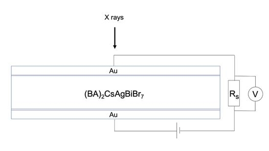
3.4. X-ray Photoresponse

Figure 5a shows almost linear dependence of the photocurrent (10−10 A) on the X-ray tube current for both of the −10 V bias voltages at the fixed sample to X-ray source separation distance of 1000 mm; however, there was a significant time instability in photocurrents for the tube currents at 10 mA and above. We attribute this to imperfections of the contact electrodes and significant charging of the sample as a result of a strong radiation field at a given polarity. The relationship between the sample current and the bias voltage from −20 V to 20 V was determined by fixing the X-ray tube current to 5 mA and the sample-to-source distance to 1000 mm (Figure 5b). The IV curve is, in general, symmetrical over the entire voltage range.

4. Discussion

Crystal growth yielded citron-yellow ca. 3 × 4 × 0.75 mm3 single crystals of 2D, layered double perovskite (BA)2CsAgBiBr7 radiation sensor material. The rectangular top and bottom crystal faces exhibited strained lattices, intermittent growth and dissolution stages in overgrowth zones surrounding the seed. A higher density of defects, especially of the inclusions and impurities, was typically concentrated on the bottom crystal faces. The PXRD and the single crystal XRD measurement results were consistent with those in the literature [13,14].
In the mid-to-high voltage range, fluctuations in the IV curves measured in both scan directions were common for all sample contacts (Figure 4). This behaviour can be attributed to drift and diffusion of charge carriers and in particular to migration of the BA+ cations and Br anions and their accumulation at an anode and cathode (saturation current). Similar to the vacancy point defects in single crystals of Cs2AgBiBr6 [7], the VBr and VBA have lower diffusion barriers and shorter migration distances compared to the VCs, VAg and VBi. Other explanations include the surface conductivity effect of the two opposite crystal faces characterised by different growth features and defects (dislocations, twin planes, cracks, inclusions and precipitates). The mismatch in the maxima values of the measured IV curves also reflects the nature of the samples, which is described above. However, a possibility of formation of an injection barrier associated with degradation of the double perovskite material in the vicinity of the Ag electrode [23] at the bias voltages approaching 100 V cannot be excluded.
The ρ values of the four samples determined from the IV measurements were 4.19 × 10¹¹–2.67 × 10¹² Ωcm, whereas those determined from the van der Pauw measurements were 1.65–9.16 × 10¹⁰ Ωcm. This discrepancy in the ρ values can be explained in terms of the chemical composition and crystal structure of the (BA)2CsAgBiBr7. In the IV method, the current is measured through the seed and along the <001> direction that is co-parallel to the arrangement of the long chains of BA+ organic cations, which provide resistance to the current flow. In contrast, in van der Pauw geometry, the current flows along the overgrowth edges of the crystal face with (001) planes that contains more conductive inorganic [AgBr6]5− and [BiBr6]3− octahedra with the Br anions electrostatically interacting with the Cs+ cations. Hence, the electrical performance of (BA)2CsAgBiBr7 is governed by its chemical composition and 2D layered crystal structure. The ρ values obtained in this study are up to one order of magnitude higher than the published value of 1.15 × 10¹¹ Ωcm [14]. The μ values 10−5–10−4 cm2V–1s–1 are low. The n t r a p values of 1.12–1.76 × 1011 cm–3 were calculated using the VTFL values derived from the IV segments in the mid-voltage range (30–50 V), i.e., the intersections between the TFL IV regime and the SCLC IV regime [23]. However, the n t r a p values are slightly higher than the literature value of 4.2 × 1010 cm–3 [14]. Improvements in the crystal growth (control of crystal growth parameters) are required to increase the size and quality of the crystals and in turn reduce the density and distribution of defects. Understanding of charge-carrier transport remains inconclusive due to the mixed ionic and electronic nature of these materials and the nature of the contacts.
In this study, the X-ray detection performance was investigated in terms of the photocurrent dependence on the applied bias, tube current and the source–sample distance. However, at this stage, no sensitivity or dose rates were assessed. Our research study contributes to a better understanding of the impressive potential of the (BA)2CsAgBiBr7 double perovskite material in radiation detection.

Supplementary Materials

The following are available online at https://www.mdpi.com/article/10.3390/cryst11101208/s1, Figure S1: The IV measurement setup using the Keithley test fixture model 8101 4TRX and triax cables connected to the Keithley SMU 2450: Ag glue electrodes deposited on the bottom and top crystal faces of the sample (BA)2CsAgBiBr7_Exp1 and connected by 0.05 mm Au wires to two 0.5 mm copper wires inserted inside the shielded test fixture (a). The van der Pauw measurement setup using the shielded test fixture and triax cables connected to the SMU 2450 and 6517B: Ag electrodes deposited at equally spaced four corners of the crystal face of the (BA)2CsAgBiBr7_Exp1 (b) and contacted via 0.05 mm Au wires to four 0.5 mm copper wires. The test fixture was covered by Al foil to prevent photogeneration of charge carriers, Figure S2: Sample (BA)2CsAgBiBr7_Exp2 (top right corner, 4 × 4 × 0.75 mm3) has a top crystal surface (a) and bottom surface (b) characterised by irregular growth and dissolution features (image on the left made in reflected light and image on the right made in transmitted light). Strained lattice and defects such as twin planes characterise a top crystal face (c) and bottom crystal face (d) of sample (BA)2CsAgBiBr7_Exp3 (3.5 × 3.5 × 0.75 mm3). The density of inclusions and precipitates is irregular and they tend to appear in clusters across the crystal faces of the two samples, Table S1: Selected crystallographic data.

Author Contributions

Data curation, investigation, methodology, formal analysis, validation, writing—original draft, writing—review and editing, V.M.; crystal growth, XRD measurements, review and editing, C.S. and M.D.; X-ray photoresponse measurements, data processing, manuscript review, V.D.; project administration, supervision, review, M.F., H.H. and J.F. All authors have read and agreed to the published version of the manuscript.

Funding

This research received no external funding.

Acknowledgments

We thank Thilo Ludwig (IAAC) for the XRD measurements with Bruker’s D8 Discover and Jiaona Zou (FMF) for the initial assistance with the Zeiss Axio Imager and the Keithley instrument setup.

Conflicts of Interest

The authors declare no conflict of interest.

References

  1. Wei, H.; Fang, Y.; Mulligan, P.; Chuirazzi, W.; Fang, H.-H.; Wang, C.; Ecker, B.R.; Gao, Y.; Loi, M.A.; Cao, L.; et al. Sensitive X-ray Detectors Made of Methylammonium Lead Tribromide Perovskite Single Crystals. Nat. Photonics 2016, 10, 333–339. [Google Scholar] [CrossRef]
  2. Li, L.; Liu, X.; Zhang, H.; Zhang, B.; Jie, W.; Sellin, P.J.; Hu, C.; Zeng, G.; Xu, Y. Enhanced X-ray Sensitivity of MAPbBr3 Detector by Tailoring the Interface-States Density. ACS Appl. Mater. Interfaces 2019, 11, 7522–7528. [Google Scholar] [CrossRef]
  3. Geng, X.; Feng, Q.; Zhao, R.; Hirtz, T.; Dun, G.; Yan, Z.; Ren, J.; Zhang, H.; Liang, R.; Tian, H.; et al. High-Quality Single Crystal Perovskite for Highly Sensitive X-Ray Detector. IEEE Electron. Device Lett. 2020, 41, 256–259. [Google Scholar] [CrossRef]
  4. Xu, Q.; Shao, W.; Li, Y.; Zhang, X.; Ouyang, X.; Liu, J.; Liu, B.; Wu, Z.; Ouyang, X.; Tang, X.; et al. High-Performance Surface Barrier X-Ray Detector Based on Methylammonium Lead Tribromide Single Crystals. ACS Appl. Mater. Interfaces 2019, 11, 9679–9684. [Google Scholar] [CrossRef]
  5. Ye, F.; Lin, H.; Wu, H.; Zhu, L.; Huang, Z.; Ouyang, D.; Niu, G.; Choy, W.C.H. High-Quality Cuboid CH3NH3PbI3 Single Crystals for High Performance X-Ray and Photon Detectors. Adv. Funct. Mater. 2019, 29, 1806984–1806991. [Google Scholar] [CrossRef]
  6. Murgulov, V.; Daub, M.; Hillebrecht, H.; Fiederle, M.; Franc, J.; Dědič, V. Growth and Characterization of Radiation Sensors Based on Single Crystals of Hybrid Metal–Organic Methylammonium Lead Bromide and Iodide Perovskite. Cryst. Res. Technol. 2020, 55, 2000112–2000124. [Google Scholar] [CrossRef]
  7. Pan, W.; Wu, H.; Luo, J.; Deng, Z.; Ge, C.; Chen, C.; Jiang, X.; Yin, W.-J.; Niu, G.; Zhu, L.; et al. Cs2AgBiBr6 Single-Crystal X-Ray Detectors with a Low Detection Limit. Nat. Photonics 2017, 11, 726–732. [Google Scholar] [CrossRef]
  8. Yin, L.; Wu, H.; Pan, W.; Yang, B.; Li, P.; Luo, J.; Niu, G.; Tang, J. Controlled Cooling for Synthesis of Cs2AgBiBr6 Single Crystals and Its Application for X-Ray Detection. Adv. Opt. Mater. 2019, 7, 1900491–1900499. [Google Scholar] [CrossRef]
  9. Yuan, W.; Niu, G.; Xian, Y.; Wu, H.; Wang, H.; Yin, H.; Liu, P.; Li, W.; Fan, J. In Situ Regulating the Order–Disorder Phase Transition in Cs2AgBiBr6 Single Crystal toward the Application in an X-Ray Detector. Adv. Funct. Mater. 2019, 29, 1900234. [Google Scholar] [CrossRef]
  10. Zhang, H.; Gao, Z.; Liang, R.; Zheng, X.; Geng, X.; Zhao, Y.; Xie, D.; Hong, J.; Tian, H.; Yang, Y.; et al. X-ray Detector Based on All-Inorganic Lead-Free Cs2AgBiBr6 Perovskite Single Crystal. IEEE Trans. Electron. Devices 2019, 66, 2224–2229. [Google Scholar] [CrossRef]
  11. Su, Y.; Ma, W.; Yang, Y. Perovskite Semiconductors for Direct X-Ray Detection and Imaging. J. Semicond. 2020, 41, 051204. [Google Scholar] [CrossRef]
  12. Wu, H.; Ge, Y.; Niu, G.; Tang, J. Metal Halide Perovskites for X-Ray Detection and Imaging. Matter 2021, 4, 144–163. [Google Scholar] [CrossRef]
  13. Connor, B.A.; Leppert, L.; Smith, M.D.; Neaton, J.B.; Karunadasa, H.I. Layered Halide Double Perovskites: Dimensional Reduction of Cs2AgBiBr6. J. Am. Chem. Soc. 2018, 140, 5235–5240. [Google Scholar] [CrossRef]
  14. Xu, Z.; Liu, X.; Li, Y.; Liu, X.; Yang, T.; Ji, C.; Han, S.; Xu, Y.; Luo, J.; Sun, Z. Exploring Lead-Free Hybrid Double Perovskite Crystals of (BA)2CsAgBiBr7 with Large Mobility-Lifetime Product toward X-Ray Detection. Angew. Chem. Int. Ed. 2019, 58, 15757–15761. [Google Scholar] [CrossRef]
  15. Zhang, W.; Zhu, H.; Pan, S.; Li, H.; Zhang, J.; Gong, Z.; Zhang, Y.; Pan, J. Growth and Properties of Centimeter-Sized Lead Free All Inorganic Perovskite Cs2AgBiBr6 Crystal by Additive CH3COONa. J. Cryst. Growth 2020, 532, 125440–125447. [Google Scholar] [CrossRef]
  16. Duijnstee, E.A.; Ball, J.M.; Le Corre, V.M.; Koster, L.J.A.; Snaith, H.J.; Lim, J. Toward Understanding Space-Charge Limited Current Measurements on Metal Halide Perovskites. ACS Energy Lett. 2020, 5, 376–384. [Google Scholar] [CrossRef]
  17. Röhr, J.A.; Kirchartz, T.; Nelson, J. On the Correct Interpretation of the Low Voltage Regime in Intrinsic Single-Carrier Devices. J. Phys. Condens. Matter 2017, 29, 205901–205910. [Google Scholar] [CrossRef]
  18. Röhr, J.A.; Moia, D.; Haque, S.A.; Kirchartz, T.; Nelson, J. Exploring the Validity and Limitations of the Mott–Gurney Law for Charge-Carrier Mobility Determination of Semiconducting Thin-Films. J. Phys. Condens. Matter 2018, 30, 105901–105914. [Google Scholar] [CrossRef] [Green Version]
  19. Röhr, J.A. Direct Determination of Built-in Voltages in Asymmetric Single-Carrier Devices. Phys. Rev. Appl. 2019, 11, 054079–054084. [Google Scholar] [CrossRef]
  20. Lampert, M.A. Simplified Theory of Space-Charge-Limited Currents in an Insulator with Traps. Phys. Rev. 1956, 103, 1648–1656. [Google Scholar] [CrossRef]
  21. Lampert, M.A.; Mark, P. Current Injections in Solids; Electrical current series; Academic Press: Cambridge, MA, USA, 1970; p. 354. [Google Scholar]
  22. Mott, N.F.; Gurney, R.W. Electronic Processes in Ionic Crystals, 2nd ed.; International Series of Monographs on Physics; Oxford University Press: Oxford, UK, 1940; p. 275. [Google Scholar]
  23. Le Corre, V.M.; Duijnstee, E.A.; El Tambouli, O.; Ball, J.M.; Snaith, H.J.; Lim, J.; Koster, L.J.A. Revealing Charge Carrier Mobility and Defect Densities in Metal Halide Perovskites via Space-Charge-Limited Current Measurements. ACS Energy Lett. 2021, 6, 1087–1094. [Google Scholar] [CrossRef]
Figure 1. A unit cell of a single crystal of BA 2 CsAgBiBr 7 double perovskite was generated based on our single crystal structure investigation and plotted using DIAMOND software.
Crystals 11 01208 g001
Figure 2. Sample (BA)2CsAgBiBr7_Exp1 (4 × 4 × 0.75 mm3) has a top crystal surface (a) and bottom surface (b) characterised by irregular growth and dissolution features (image on the left made in reflected light), strained lattice and defects such as twin planes at 90° (image on the right made in transmitted light). Sample (BA)2CsAgBiBr7_Exp4 (3.5 × 3.5 × 0.75 mm3) has more regularly spaced segregation lines in the top crystal face (c), while its bottom crystal face has a higher density of defects, such as inclusions and precipitates (d). Both crystal faces exhibit bent lattice in the overgrowth zones.
Crystals 11 01208 g002
Figure 3. PXRD pattern (Mo-Ka1 radiation source) for (BA)2CsAgBibr7 (a) and XRD patterns (Cu-Ka radiation source) for the single crystals Exp1 (bottom) and Exp 2 (top) (b).
Crystals 11 01208 g003
Figure 4. IV curves generated in the dark for the Ag- BA 2 CsAgBiBr 7 contacts. The IV curves in the forward and reverse scan directions for Ag-Exp1 lack complete symmetry (a); an SCLC regime identified in the forward scan direction (b). No clear regimes can be identified for Ag-Exp2 (c,d) and Ag-Exp3 (e,f); a very narrow SCLC regime can be identified in the reverse scan for Ag-Exp4 (g,h).
Crystals 11 01208 g004
Figure 5. Dependence of the photocurrent on the X-ray tube current at +10 V and −10 V for the Exp4 sample-to-source separation of 1000 mm (a). Relationship between the Exp4 sample current and the Exp4 sample bias determined at 5 mA X-ray tube current and the sample-to-source separation of 1000 mm (b).
Crystals 11 01208 g005
Table 1. Key electrical parameters derived from the IV curves for the (BA)2CsAgBiBr7 sample using Ag glue electrodes.
SampleContactsL (mm)U (V)ρ (Ωcm)VTFL (V)μ (cm2V−1s−1)ntrap (cm−3)
Exp1T+ B−0.75−3 to 201.14 × 101237.43.20 × 10−51.32 × 10¹¹
43.38.65 × 10−51.53 × 10¹¹
B+ T−1.45 × 10¹²
Exp2T+ B−0.75−30 to 84.19 × 10¹¹
B+ T−5.40 × 10¹¹
Exp3T+ B−0.75−100 to 1002.67 × 1012
B+ T−2.56 × 10¹²
Exp4T+ B−0.75−36 to 327.09 × 101149.99.11 × 10−51.76 × 10¹¹
B+ T−6.94 × 101131.71.34 × 10−41.12 × 10¹¹
33.11.44 × 10−41.17 × 10¹¹
Sample thickness L; trap-filled limit voltage V T F L ; density of trap states n t r a p ; resistivity ρ ; ohmic voltage range U; permittivity of vacuum ε o of 8.85 × 10⁻¹⁴ Fcm−1; relative permittivity of (BA)2CsAgBiBr7  ε r of 18 [14]; elementary charge q of 1.602176 × 10⁻¹⁹ Ce−1. Top crystal face T; bottom crystal face B.
Table 2. Specific resistivity values derived from the van der Pauw measurements.
SampleSetupρ (Ωcm)
Exp1-Ag glue27.67 × 1010
16.99 × 10¹⁰
33.03 × 10¹⁰
Exp2-Ag glue29.16 × 1010
16.99 × 10¹⁰
32.06 × 10¹⁰
Exp3-Ag glue28.90 × 1010
33.41 × 10¹⁰
15.80 × 10⁹
Exp4-Ag glue23.01 × 1010
12.19 × 10¹⁰
31.65 × 10¹⁰
Specific resistivity ρ ; setup: (1) the SMU 2450 in a constant current source (10 pA) and measure voltage mode; (2) the SMU 2450 in a constant voltage source (5 V) and measure current mode; (3) the electrometer 6517B as a voltage source (0.1 V) and an ammeter with the SMU 2450 as a voltmeter.
Publisher’s Note: MDPI stays neutral with regard to jurisdictional claims in published maps and institutional affiliations.

